

Page 1
17" LCD Colour Monitor
Service
Service
Service
SH4 HP L1740
CJ6B50/76
CJ6B50/02
Horizontal frequencies
30 - 83 kHz
TABLE OF CONTENTS
Description Page
Important Safety Notice---- -------------------------- 2
Technical Data --------------------------------------3~6
Installation/On Screen Display-------------------7~10
Warning Message-------------------------------------11
Factory Mode------------------------------------------12
Flat Panel adjust--------------------------------------13
Trouble shooting--------------------------------------14
Mechanical Instructions-------------------------15~16
Definition of pixel defects----------------------------17
Electrical Instructions---------------------------18~19
Failure mode of panel---------------------------------20
Display adjustment-----------------------------------21
Safety test requirements-----------------------------22
SAFETY NOTICE
ANY PERSON ATTEMPTING TO SERVICE THIS CHASSIS MUST FAMILIARIZE HIMSELF WITH THE CHASSIS
AND BE AWARE OF THE NECESSARY SAFETY PRECAUTIONS TO BE USED WHEN SERVICING ELECTRONIC
EQUIPMENT CONTAINING HIGH VOLTAGES.
Description Page
DDC Instructions/DATA-------------------------23~31
ISP Instructions---------------------------------32~34
Repair tips/Repair Flow chart------------------35~38
Wiring Diagram---------------------------------------39
Function Block----------------------------------------40
Scaler Diagram----------------------------------41~45
Scaler Board C.B.A------------------------------46~47
Control Diagram & C.B.A.----------------------------48
Power Diagram ----------.-----------------------49~54
Exploded View--------------------------------------- 55
Recommended/Spare parts list----------------56~58
General product specification------------------59~90
Different parts list------------------------------------91
CAUTION: USE A SEPARATE ISOLATION TRANSFORMER FOR THIS UNIT WHEN SERVICING.
REFER TO BACK COVER FOR IMPORTANT SAFETY GUIDELINES
Published by BCU Monitors Printed in Suzhou Copyright reserved Subject to modification F Nov .11 2004
GB
3138 106 10438
Page 2

2
HP L1740
Important Safety Notice
Go to cover page
Proper service and repair isimportant to the safe, reliable
operation of all HPConsumer Electronics Company**
Equipment. The service procedures recommended by HP and
described in this service manual are effective methods of
performing service operations. Some ofthese service
operations require the use of tools specially designed for the
purpose. The special tools should be used when and as
recommended.
It is important to note that this manual contains various
CAUTIONS and NOTICES which should be carefully read in
order to minimize the risk of personal injury to service
personnel. The possibility exists that improper service
methods may damage the equipment. It is also important to
understand that these CAUTIONS and NOTICES ARE NOT
EXHAUSTIVE. HP could not possibly know, evaluate and
advise the service trade of all conceivable ways in which
service might be done or of the possible hazardous
consequences of each way. Consequently, HP has not
undertaken any such broad evaluation. Accordingly, a
servicer who uses a service procedure or tool which is not
recommended by HP must first satisfy himself thoroughly that
neither his safety nor the safe operation of the equipment will
be jeopardized by the service method selected.
* * Hereafter throughout this manual, HP Consumer
Electronics Company will bereferred to as HP.
WARNING
Critical components having special safety characteristics are
identified with a bythe Ref. No. inthe parts list and
enclosed within a broken line*
(where several critical components are grouped in one area)
along with the safety symbol on the schematics or
exploded views.
Use of substitute replacement parts which do not have the
same specified safety characteristics may create shock, fire,
or other hazards.
Under no circumstances should the original design be
modified or altered without written permission from Philips.
Philips assumes no liability, express or implied, arising out of
any unauthorized modification of design.
Servicer assumes all liability.
*BrokenLine
FOR PRODUCTS CONTAINING LASER :
DANGER- Invisible laser radiation when open.
AVOID DIRECT EXPOSURE TO BEAM.
CAUTION- Use of controls or adjustments or
performance of procedures other than
those specified herein may result in
hazardous radiation exposure.
CAUTION- The use of optical instruments with this
product will increase eye hazard.
TO ENSURE THE CONTINUED RELIABILITY OF THIS
PRODUCT, USE ONLY ORIGINAL MANUFACTURER'S
REPLACEMENT PARTS, WHICH ARE LISTED WITH THEIR PART
NUMBERS IN THE PARTS LIST SECTION OF THIS
SERVICE MANUAL.
Take care during handling the LCD module with backlight
unit
- Must mount the moduleusing mounting holes arranged infour
corners.
- Do not press onthe panel, edge of theframe strongly or electric
shock as this will result in damage to the screen.
- Do not scratch orpress on the panel withany sharp objects, such
as pencil or pen asthis may result in damage to the panel.
- Protect the module fromthe ESD as it maydamage the electronic
circuit (C-MOS).
- Make certain that treatment person s body are grounded through
wrist band.
- Do not leave themodule in high temperature andin areas of high
humidity for a long time.
- Avoid contact with water as it may ashort circuit within the module.
- If the surface ofpanel become dirty, please wipe it off with a soft
material. (Cleaning with a dirty or rough cloth may damage the
panel.)
Page 3
Technical Data
"
HP L1740
Go to cover page
3
Page 4
4
HP L1740
Technical Data(Continued)
Go to cover page
2. Electrical characteristics and performance
Test signal and test method in accordance with test instructions sheet
161 of the product where applicable.
2.1 Actual display size: 337.920 x 270.336 mm
2.2 Resolution
1.Factory Preset modes (15 modes)
# Resolution H-Frequency
(Hz)
1 640X480 31.469K 25.175 59.940 Hz VGA
2 640X480 37.861K 31.5 72.809 Hz VESA
3 640X480 37.5K 31.501 75 Hz VESA
4 720X400 31.469K 28.322 70.087 Hz VGA
5 800X600 37.879K 40 60.317 Hz VESA
6 800X600 48.077K 50 72.188 Hz VESA
7 800X600 46.875K 49.498 75 Hz VESA
8 832X624 49.726K 57.284 74.551 Hz MAC
9 1024X768 48.363K 65 60.004 Hz VESA
10 1024X768 56.476K 75 70.069 Hz VESA
11 1024X768 60.023K 78.75 75.029 Hz VESA
12 1152X870 68.68K 100 75.06 Hz MAC
13 1152X900 71.71K 108 76.05 Hz SUN
Pixel rate
(MHz)
V-Frequency Comment
2.5
14 1280X1024 63.98K 108 60.02Hz VESA
15 1280X1024 79.97K 135 75.02Hz VESA
Over-scan Mode
16 640*480 43.269K 36.000 85.008Hz
Page 5
Technical Data(continued)
HP L1740
Go to cover page
5
2.12
2.13
2.14
Page 6

6
HP L1740
Go to cover page
Technical Data(Continued)
Page 7
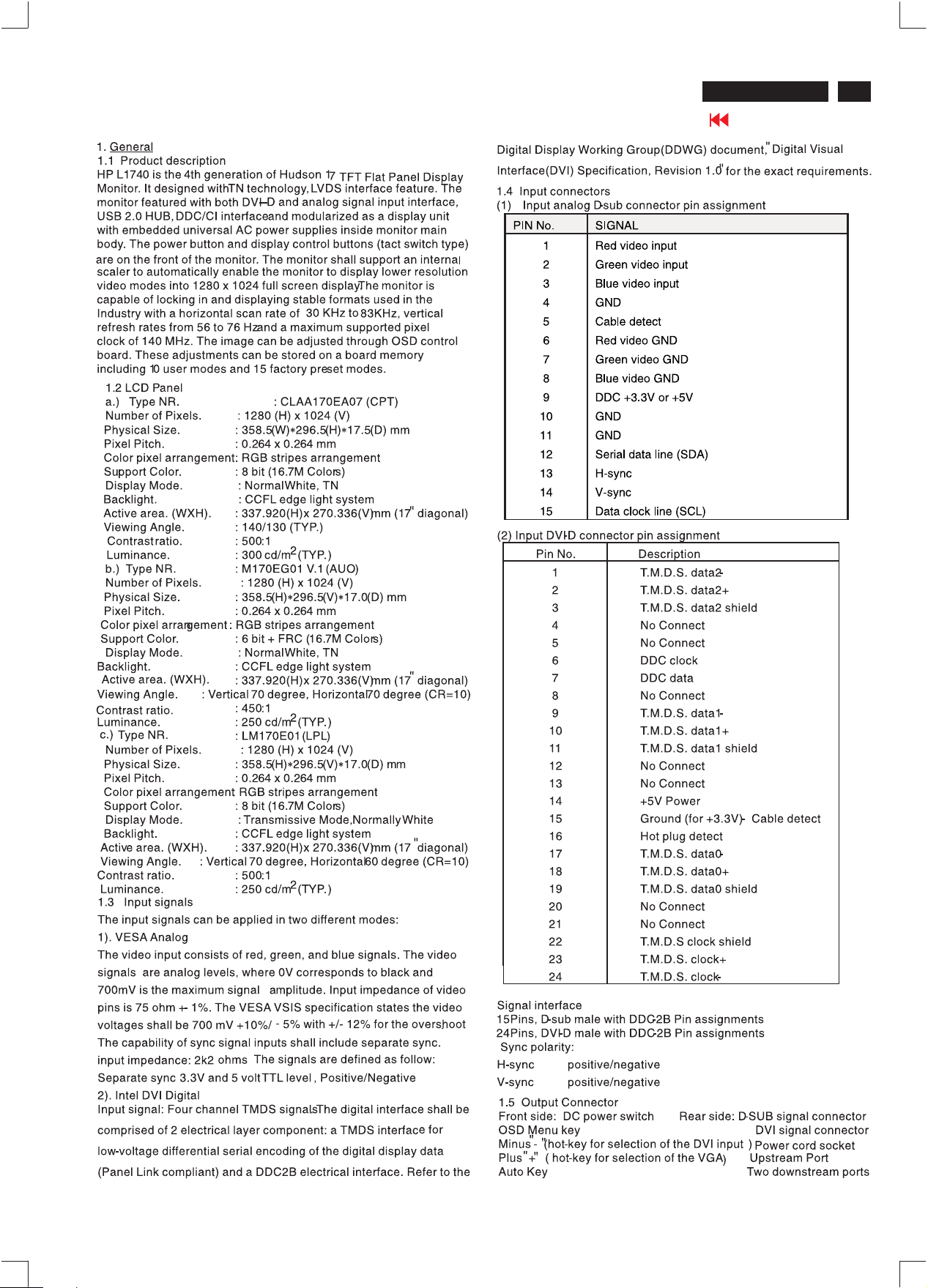
Installation
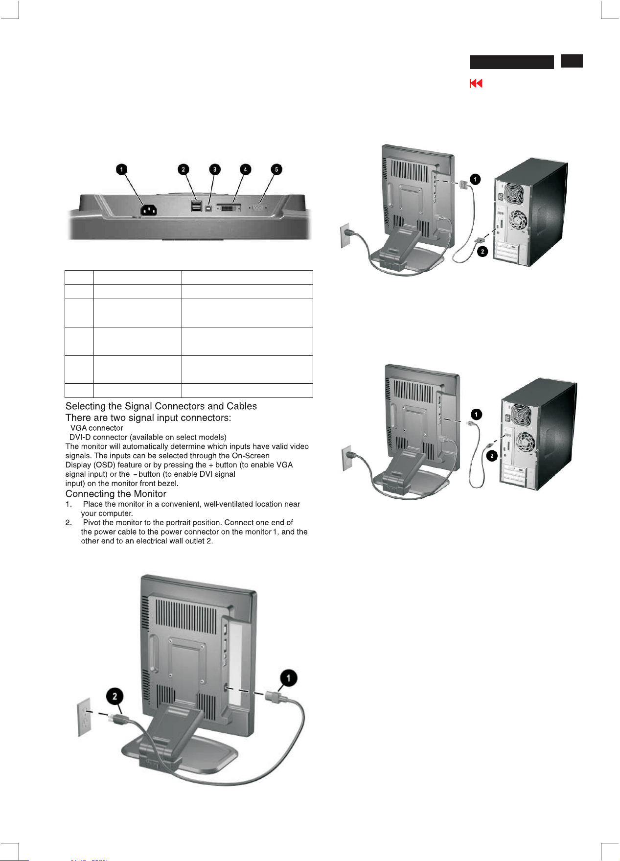
Rear Panel Components
No Component Function
1 AC power connector Connects the AC power cord to the monitor
2 USB downstream connectors Connects optional USB devices
to the monitor
3 USB upstream connector Connects the USB cable to the host
(computer or another USB hub)
4 DVI connector (available on
select models)
5 VGA connector Connects the VGA cable to the monitor
. Connects the DVI -D signal cable to the
monitor
HPL 1740
Go to cover page
3. For analog operation, connect one end of the VGA signal
cable to the VGA connector on the monitor 1, and the other
end to the VGA connector on the computer 2.
Connecting the VGA Signal Cable
4. Connect the USB cable to the USB upstream connector on the
monitor 1 and to a convenient USB connector on the computer 2.
7
Connecting the Power Cable
Connecting the USB Cable
Page 8
8
HP L1740
Go to cover page
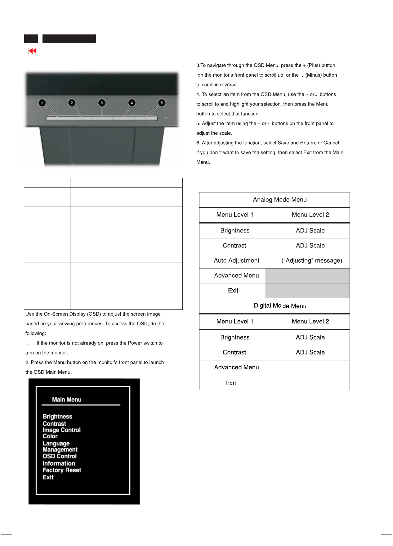
Front Pan el Controls
On Screen Display
No Control Function
1 Auto Adjust Activates the auto adjustment feature for optimum
image
2 Menu Opens the On-Screen Display (OSD) menu
3 – (Minus) If OSD is on, press to navigate backward through
-
the OSD menu features and decrease adjustment
levels.
If OSD is off, press to enable the DVI signal input
(available on select models)
4 + (Plus) If OSD is on, press to navigate forward through the
OSD menu features and increase adjustment
levels
If OSD is off, press to enable the VGA signal input
5 Power Turns the monitor on or off
BASIC OSD MENU LEVEL S
Page 9
On Screen Display
ADVANCED OSD MENU LEVELS
Analog Mode Menu
Menu Level 1 Menu Level 2 Menu Level 3 Factory Reset?
Brightness ADJ Scale Y(90)
Contrast ADJ Scale Y(80)
Image Control Auto Adjustment ( Adjusting message) Y (no FD)
Horizontal Position ADJ Scale Y (no FD)
Vertical Position ADJ Scale Y (no FD)
Clock ADJ Scale Y (no FD)
Clock Phase ADJ Scale Y (no FD)
Cancel
Save and Return
Color 9300 K
6500 K Y(FD)
Custom Color Custom Color ADJ
SRGB
Cancel
Save and Return
Language Deutsch
S. Chinese
English N (FD=English)
Espanol
Francais
Italiano
Nederlands
Cancel
Save and Return
Management Power Saver On / Off Selection N (FD=ON)
Power On Recall On / Off Selection N (FD=ON)
Mode Display On / Off Selection N (FD=OFF)
Power-On Status display On / Off Selection N (FD=ON)
Sleep timer Timer Set Menu N (FD=0;OFF)
""
HPL 1740
Go to cover page
9
Default Video Input -Analog - VGA N (FD = DVI)
-Digital - DVI
Serial Number Display monitor s/n
Basic Menu N(FD=Basic)
Cancel
Save and Return
OSD Control Horizontal OSD Position ADJ Scale N (FD=50)
Vertical OSD Position ADJ Scale N (FD=50)
OSD Timeout ADJ Scale N (FD=30)
Cancel
Save and Return
Information Current Settings:
Recommended Settings:
Serial Number:
Total Hours:
Backlight Hours:
Exit
Factory Reset Yes
No
Exit
Page 10
10
HP L1740
Go to cover page
On Screen Display
Digital Mode Menu
Menu Level 1 Menu Level 2 Menu Level 3 Factory Reset?
Brightness ADJ Scale Y (90)
Contrast ADJ Scale Y (80)
Color 9300 K
6500 K Y(FD)
Custom Color Custom Color ADJ
SRGB
Cancel
Save and Return
Language Deutsch
S. Chinese
English N (FD=English)
Español
Français
Italiano
Nederlands
Cancel
Save and Return
Management Power Saver On / Off Selection N(FD=ON)
Power On Recall On / Off Selection N(FD=ON)
Mode Display On / Off Selection N (FD=OFF)
Power-On Status Display On / Off Selection N(FD=ON)
Sleep Timer Timer Set Menu
Default Video Input -Analog - VGA N(FD=DVI)
-Digital - DVI
Serial Number Display monitor s/n
Basic Menu N(FD=Basic)
Cancel
Save and Return
OSD Control Horizontal OSD Position ADJ Scale N (FD=50)
Vertical OSD Position ADJ Scale N (FD=50)
OSD Timeout ADJ Scale N (FD=30)
Cancel
Save and Return
Information Current Settings: Yes
Recommended Settings:
Serial Number:
Total Hours:
Backlight Hours:
Exit
Factory Reset Yes
No
Exit
NOTE:
Unless designated by “FD”, the original factory default settings
""
are identical to the user Factory Reset function.
Page 11

Warning Message
HPL 1740
Go to cover page
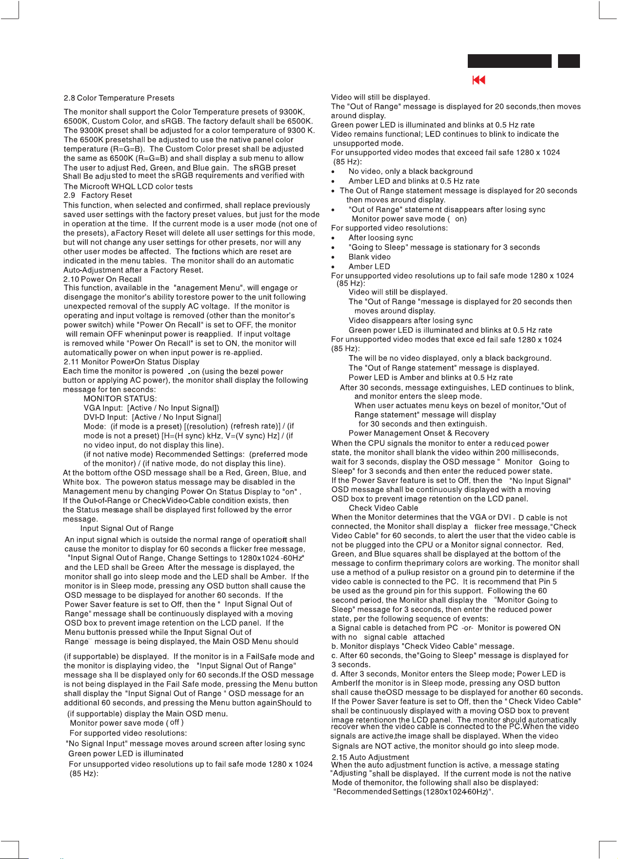
Item Attention Signals Display Time Condition
1 Input Signal out of Range See section power saver
2 No Input Signal See section power saver
3 Going to Sleep See section power saver
4 Adjusting Auto hot key or OSD menu function
5OSDLock out 3secs Push menu key for 10 sec then display 3 sec WM OSD Lock out
6 Input Not Available DVI (Analog) switch to Analog (DVI) without sync
7 Check Video Cable See section power saver
""
Power saver
Power Saver - On Power Saver - Off Note
Quit signal with
cable 1. System blank and show WM Going
Disconnect cable
to Sleep 3 sec then sleep.
"
1. System blank and show WM Check
Video Cable 10 sec then moving about
50 sec.
2. Show WM Going to Sleep 3 sec then
sleep.
3. If push any key in sleep mode, then
repeat item 1 to 2.
"
"
1. System blank and show moving
WM No Input Signal always.
"
1. System blank and show WM
Check Video Cable 10 sec then
""
moving always.
"
"
11
Out of range 1
Out of range 2
Out of range 3
-
-
-
1. System blank and show moving WM
Input Signal out of Range about 60
"
sec.
2. Show WM Going to Sleep 3 sec
then sleep.
3. If push any key in sleep mode, then
repeat item 1to 2.
1. Show moving WM Input Signal out of
Range 60 sec.
2. WM disappear after WM 60 sec.
3. IF push any key then repeat 1-2.
1. Show moving WM Input Signal out
of Range 60 sec.
2. After moving WM 60 sec then show
WM Going to Sleep 3 sec then sleep.
"
3. If push any key in sleep mode, then
repeat item 1 to 2.
"
"
"
"
"
"
"
"
1. System blank and show moving
WM Input Signal out of Range
"
always.
1. Show moving WM Input Signal
out of Range 60 sec.
2. WM disappear after WM 60 sec.
3. IF push any key then repeat 1-2.
1. Show moving WM Input Signal
out of Range 60 sec.
2. After moving WM 60 sec then
show WM Going to Sleep 3 sec
then sleep.
3. If push any key in sleep mode,
then repeat item 1 to 2.
"
"
"
"
"
"
H<29.5 or
H>92 or
"
90>H>82.5
or V<49or
V>87 or
Vtotal>=1200
DownScaling
Ex.
1280x1024
(Only for
HPL1530)
85Hz
Page 12
12
HP L1740
Go to cover page
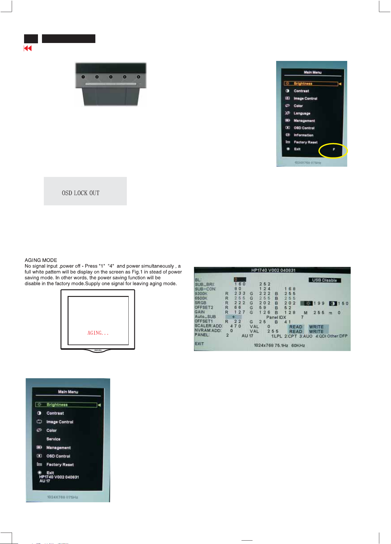
Lock/Unlock,Aging, Service/Factory Mode
Front control panel
To Lock/Unlock OSDfunction
The OSDfunction can be locked by pressing MANU button for
more than 10 seconds,the screen shows following windows for 3
seconds. Everytime when you press MANU OrAUTO
button, thismessage AppearsOnthe screen automatically.
The POWER & INPUThotkey are still functional for
POWER and INPUT expectively while OS
Locked OSDfunction can be released by pressing MANU
button for more than 10 seconds. While press MANU button for
OSDunlocked purpose, the screen will keep showing OSD LOCK
OUTuntil OSDfunction unlocked and the windows screen
automatically showed .
" 5 "
"3"
D locked.
""
2
" 2 " "1 "
" 2 "
Access Factory Mode
Power off on the monitor,
To hold Auto And
+"+" buttons at the
sametime,
And press POWER
button to power on the monitor.
Press MANU button to
bring up OSDmenufor
confirmation
Factory menu
Cursor can move on gray color area
BL :Blacklevel value
SUB-BRI : Brightness value range(Min Max)
SUB-CON : Contrast value range(Min Mid Max)
SRGB-B : Brightness of sRGB(Reserved)
SRGB-C : Contrastof sRGB(Reserved)
Gain-m : Minimum valueof User Gain
Gain-M : Maximum valueof User Gain
AUTO-SUB:TodoAuto color function when push Up key in white
Panel T
ype :Ifset this to 1,2,3,4,5 then systemwill force panel type
SCALER : Read/Write scaler register
NVRAM :Read/Write eeprom address
"1"
" 4 "
""
pattern
to LG(QDI), CPT or AU). Set to other value will auto
detect panel based on panel hardware.
Fig.1
SERVICE MODE
Press and hold the ManuPower off
Into the service mode.Press Manubutton to bring up OSD
menufor confirmation asbelow:
"2"
" 2 "
Power
-> on ,then
" 5 "
Page 13

Flat Panel Adjust
HP ADJUSTMENT PATTERN.EXE
VERSION: 2.00 Rev A
OPERATING SYSTEM(S):
Microsoft Windows 98
Microsoft Windows Millennium Edition (ME)
Microsoft Windows 2000
Microsoft Windows XP 32-bit Personal
Microsoft Windows XP 32-bit Professional
DESCRIPTION: This CD contains the HP Auto-Adjustment utility, which is a
single pattern program designed to help improve the picture quality of your HP
flat panel monitor.
Note: Do not use the following procedure if your flat panel monitor is using a
DVI connector option.
To use the Adjustment pattern with your flat panel monitor:
1. Execute the auto-adjust function from the OSD main menu.
2. If the result is not satisfactory, start the "Adjustment pattern.exe" program
and repeat step 1.
HP L1740
Go to cover page
13
Image quality characteristics that can be improved:
- Fuzzy or unclear focus
- Ghosting, streaking or shadowing effects
- Faint vertical bars
- Thin horizontal scrolling lines
- Centering the picture
Note: To achieve optimal picture performance, it is recommended that you
always set the operating system display mode to your flat panel's native
resolution. See list below for reference.
14in. and 15in. flat panels = 1024x768
17in., 18in. and 19in. flat panels = 1280x1024
20in. and 21in. flat panels = 1600x1200
Page 14
14
HP L1740
Trouble shooting
Go to cover page
The following table lists possible problems, the possible cause of each problem, and the recommended
solutions.
ProblemPossible Cause Solution
Screen is blank. Power cord is
Image appears
blurred, indistinct, or
too dark.
Image is not
centered.
disconnected.
Power switchonfront
panel of the monitor is
turned off.
Video cable is
improperlyconnected.
Screen blanking utility is active.
Brightness andcontrast
are too low.
Position may need
adjustment.
Connectthepower cord.
Press the front panel power
button.
Connectthevideo cable
properly. Refer to
Setting Up th e Moni to r, for
more information.
Press anykey on the
keyboard or movethe
mouse to inactivate the
screen blanking utility.
Press the Auto Adjust button
on the front panel.Ifthis
does not correcttheimage,
press the Menu button to
open the BasicOSDMenu,
and adjust the brightness
andcontrast scales as
needed.
Press the Menubuttonto
access the OSD menu.
Select Image Control/
Horizontal Position or
Vertical Position to adjust the
horizontalorvertical
position of the image.
"
Check Signal
"
Cable is displayed
on screen.
Out ofRange.Set
Monitor to 1280 x
1024 @ 60Hz is
displayed on screen.
Monitor video cable is
disconnected.
Video resolution and/or
refresh rate are set
higher than what your
monitor supports.
Connectthe15-pin monitor
video cable to the VGA
connector on the computer,
or, ifconnected, check the
DVI-D signal cable to the
DVI connector on the
computer, or the VGA to
DVI-I cabletotheVGA
connector on the computer
(DVI availa
models only). Besurethat
the computer power is off
while connecting the video
cable.
Restart your computer and
enter Safe Mode.Change
your settings to a supported
setting (see FactoryPreset
Display Modes table in
Appen
computer so that the new
settings takeeffect.
ble on select
"
"
dixB).Restart your
Page 15
14
Front view
Back view
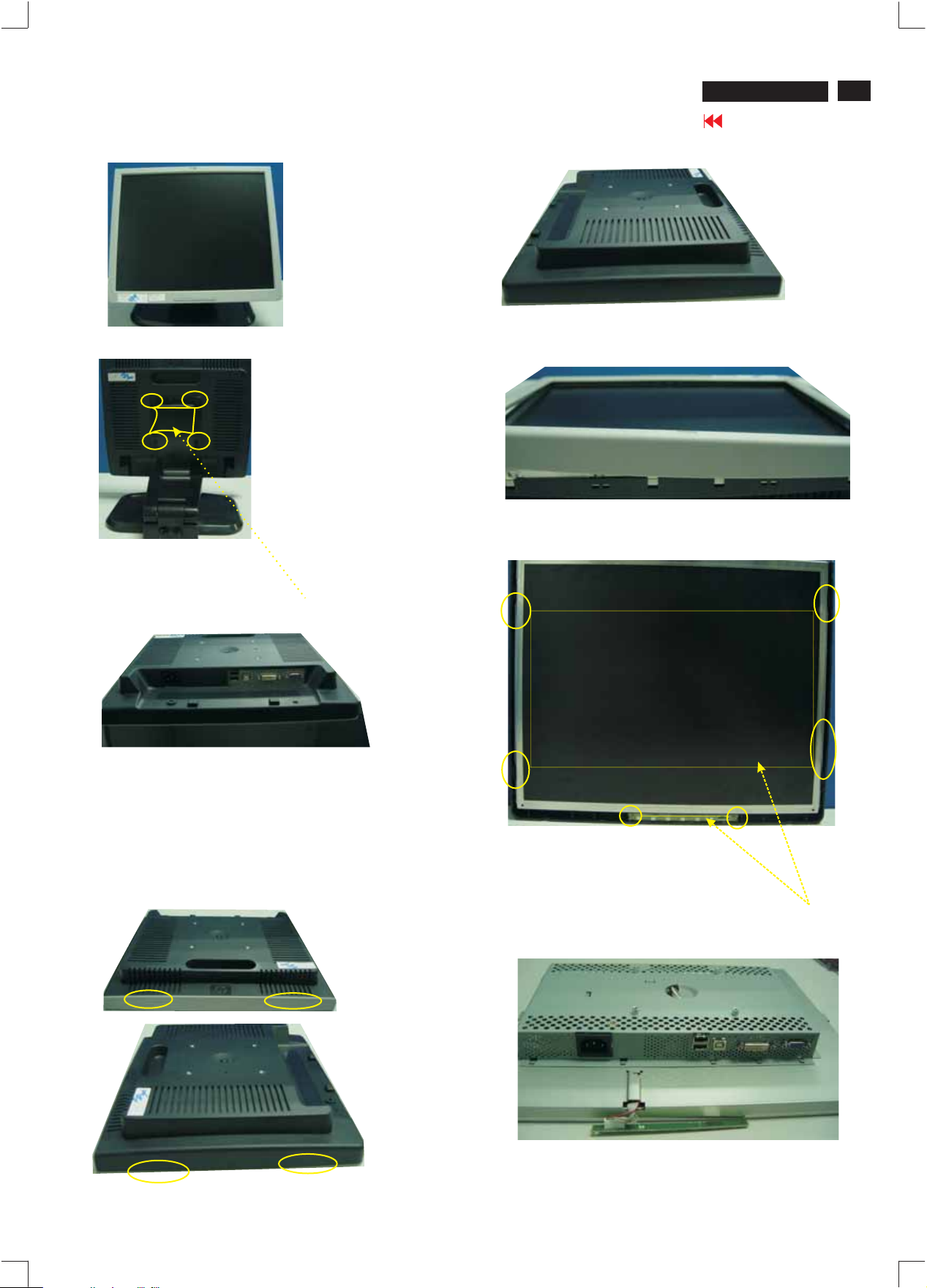
Mechanical Instruction
Fig.1
Fig.2
HPL 1740
Go to cover page
Fig.6
15
Step 1.Remove the base
Remove the four screws as Fig.2.Fig.3
Step 2. Remove the front cover as Fig.4~8.
a. Use thin "I" type screwdriver to open the clicks on top
sides as Fig.4
b .Use thin "I" type screwdriver to open the clicks on right
side as Fig.5
c. Use thin "I" type screwdriver to open 4 clicks on left
side as Fig.6
Fig.7
Fig.3
Fig.8
Step 3.Remove the back cover
Open the clicks and unscrew the screws as shown in Fig.8
and then remove the back cover as shown in Fig.9
Fig.5
Fig.4
Fig.9
Page 16

16
HP L1740
Mechanical Instruction
Go to cover page
Step .4 Remove the Metal frame board
remove the screws and then pull the metal frame with the
direction as shown in Fig.10 Fig.11
Fig.10
Power board
Fig.11
Step 5. Remove the control , scaler and power board
remove the screws and disconnect the connector as shown in Fig.11
Control board
In warranty, it is not allowed to disassembly the LCD panel, even the
backlight unit defect.
Out of warranty, the replacment of backlight unit is a correct way
when the defect is cused by backlight (CCFL,Lamp).
Page 17

Definition of pixel defects
LCD Monitor Quality and Pixel Policy
The TFT monitor uses high-precision technology, manufactured according to HP standards, to guarantee
trouble-free performance. Nevertheless, the display may have cosmetic imperfections that appear as small
bright or dark spots.
This is common to all LCD displays used in products supplied by all vendors and is not specific to the HP LCD.
These imperfections are caused by one or more defective pixels or sub-pixels.
1. A pixel consists of one red, one green, and one blue sub-pixel.
2. A defective whole pixel is always turned on (a bright spot on a dark background), or it is always off (a dark spot
on a bright background). The first is the more visible of the two.3. A defective sub-pixel (dot defect) is less
2. visible than a defective whole pixeland is small and only visible on a specific background.The HP display does
not have more than:
4. bright dots.
5. dark dots.
HP L1740
Go to cover page
17
6. total bright and dark dots.
7. No more than two adjacent (less than 2.5 mm edge-to-edge) defective pixels. To locate defective pixels, the monitor
should be viewed under normal operating conditions, in normal operating mode at a supported resolution and
refresh rate, from a distance of approximately 50 cm (16 in.).HP expects that, over time, the industry will continue to
improve its ability to produce LCDs with fewer cosmetic imperfections And HP will adjust guidelines as
improvements are made.
Page 18
18
HP L1740
Go to cover page
Electrical Instructions
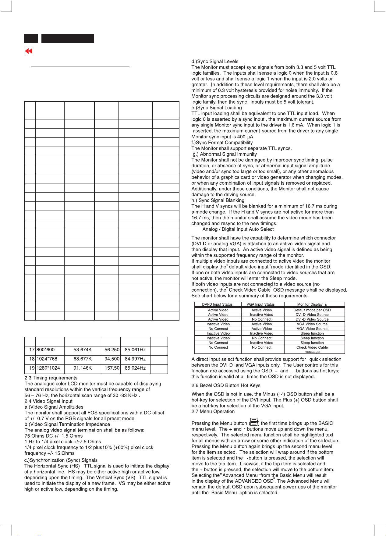
Table1 Preset Mode Resolution
# Resolution H-Frequency
1 640X480 31.469K 25.175 59.940Hz VGA
2 640X480 37.861K 31.5 72.809Hz VESA
3 640X480 37.5K 31.501 75Hz VESA
4 720X400 31.469K 28.322 70.087Hz VGA
5 800X600 37.879K 40 60.317Hz VESA
6 800X600 48.077K 50 72.188Hz VESA
7 800X600 46.875K 49.498 75Hz VESA
8 832X624 49.726K 57.284 74.551Hz MAC
9 1024X768 48.363K 65 60.004Hz VESA
10 1024X768 56.476K 75 70.069Hz VESA
11 1024X768 60.023K 78.75 75.029Hz VESA
12 1152X870 68.68K 100 75.06Hz MAC
13 1152X900 71.71K 108 76.05Hz SUN
14 1280X1024 63.98K 108 60.02Hz VESA
15 1280X1024 79.97K 135 75.02Hz VESA
(Hz)
Pixel rate
(MHz)
V-Frequency Comment
(TABLE1)
2.3 Input signal mode for over-scan modes
Table2 Over -scan Mode Resolution
# Resolution H-Frequency
(Hz)
16 640X480 43.269K 36.000 85.008Hz VESA
17 800x600 53.674K 56.250 85.061Hz VESA
18 1024x768 68.677K 94.500 84.997Hz VESA
19 1280x1024 91.146K 157.50 85.024Hz VESA
Pixel rate
(MHz)
V-Frequency Comment
Page 19

Electrical Instructions
Use Minolta CA-110 for color coordinates and luminance check.
Luminance is >200 Nits in the center of the screen when brightness at
100% and contrast set to 100% at 6500°K color temperature.
3.4 Adjustment ofWHITE-D for sRGB (B)
Apply a1280*1024 /60Hz signal withwhite pattern, then adjust
the R, G, B Sub- Gain,for t
chromaticity(X,Y)co-ordinates andY Luminance shall be:
x(center) 0.3127 ± 0.02
y(center) 0.3291 ± 0.02
Y(nits) 150 ± 10
Use Minolta CA-110 for color coordinates and luminance check.
Luminance is > 140 Nits in the center of the screen at sRGB color
temperature.
3.5 Adjustment of sRGB (B)
Apply sRGB test program, the monitor shall pass sRGB test compliance.
(Note :For sRGB compliance , the monitor shall pass either max. Delta
Elessthan or equal to 15 and a
3.6 DDC/CI Function Check(B)
Connect D-sub andDVI-D cable to the monitor.ApplyDDC/CItest
program, the monitor shall pass DDC/CItestcompliance bothfor
VGA andDVIinput.
3.7 USB Function Check(B)
Connecting cable from upstreamport of the monitor to PC systemwith
XP OS and attaching external USB devices to downstreamports of the
monitor.ApplyUSBtest program, the monitor shall pass USB test
compliance.
3.8 Settingfor leaving the Factory(B)
a).The OSD Controls shall havethe followingfactorydefault values
after finishing all the
en adjustment is finished, monitor shouldbesetto
b.) Wh
6500K color.
c.) The monitor shall leavethe factorywith the power switch
set to the OFF position
hescreencenter, the1931 CIE
sRGB
verage Delta E less than or equal to 10 )
Adjustment.
1.Menu =Basic
2. Color =6500K
3. Language = English
4. Power Saver =ON
5. Power On Recall =ON
6. Mode Display=OFF
7. Horizontal OSD Position =50%
8. Vertical OSD Position =50%
9.OSDTimeout =30
10.SleepTimer =OFF
11.Brightness = 90%
12. Contrast =80%
HP L1740
Go to cover page
19
Page 20

20
HP L1740
Failure Mode Of Panel
Go to cover page
Quick reference for failure mode of LCD panel
this page presents problems that could be made by LCD panel.
It is not necessary to repair circuit board. Simply follow the mechanical
instruction on this manual to eliminate failure by replace LCD panel.
Polarizer has bubbles
Failure description
Vertical block defect
Vertical dim lines
Vertical lines defect
(Always bright or dark)
Horizontal block defect
Phenomenon
Polarizer has bubbles
Foreign material inside
polarizer. It shows liner or
dot shape.
Concentric circle formed
Horizontal dim lines
Horizontal lines defect
(Always bright or dark)
Has bright or dark pixel
Bottom back light of LCD is
brighter than normal
Back light un-uniformity
Backlight has foreign material.
Black or white color, liner or
circular type
Page 21
Display adjustment
HPL 1740
Go to cover page
21
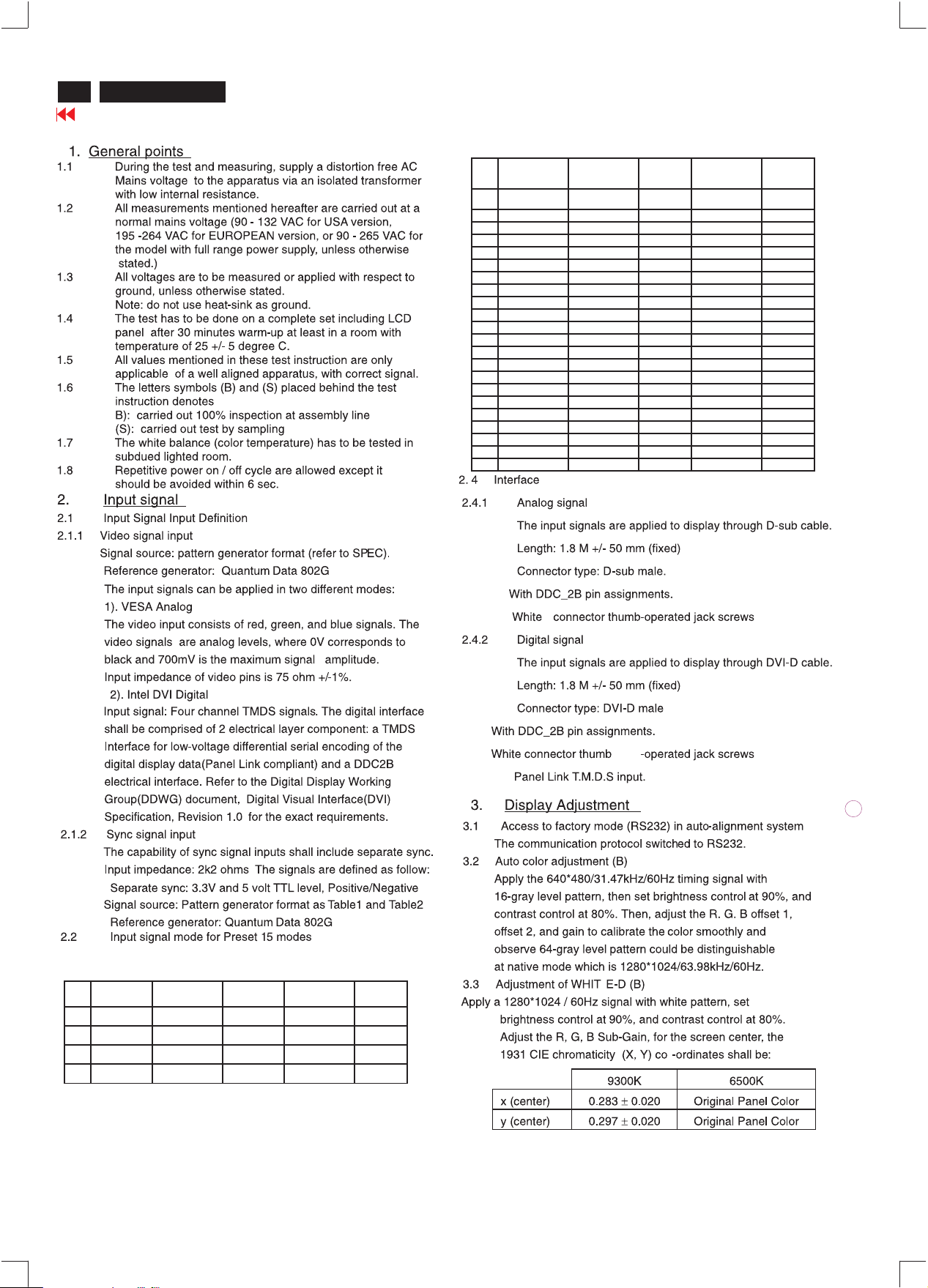
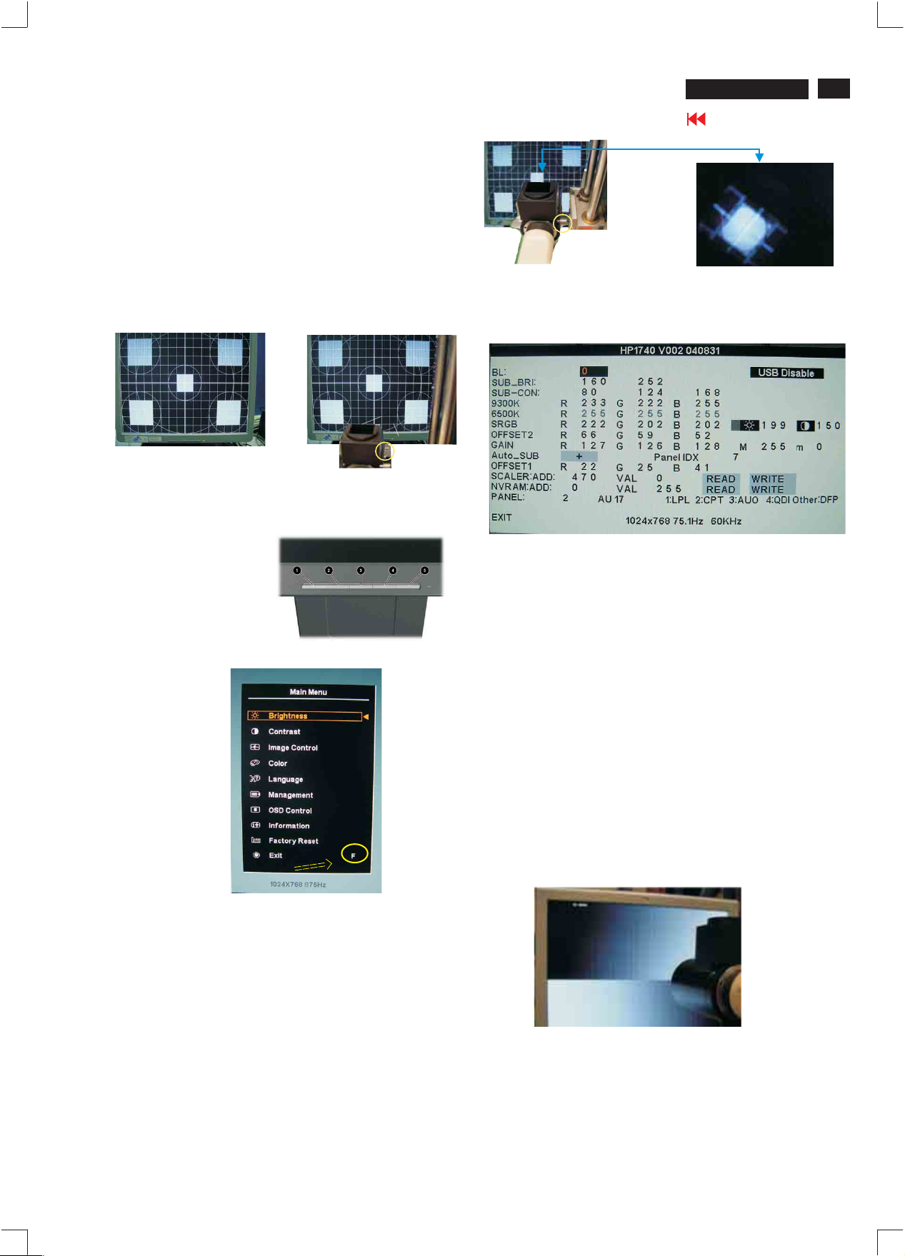
Alignment procedure
1. Turn on HP L1740 LCDmonitor.
2.Turn onthe Timing/pattern generator. See Fig.1
Resolution :1280x1024
Timing : H= 31.47KHz V=60Hz
3. Preset LCD color Analyzer CA-110
-Removethe lens protective coverofprobe CA-A30.
-Set measuring/viewing selector to measuring
analyzer.(zero calibration) as Fig.2
-Turn onthe color analyzer (CA-110)
-Press 0-CAL buttonto startingreset analyzer. S ee Fig.3
Fig. 1
4.
Access Factory Mode
Poweroffonthemonitor,
To h old AutoAnd
+"+" buttons at the
same time ,
And press POWER
buttonto poweronthemonitor.
Press MANU buttonto
bring up OSD menu for
confirmation
" 1 "
" 4 "
position for reset
Measurement viewing selector
Cover(black)
Fig. 2
Clear image
Measurement/viewing selector
Fig. 4
10. Setting patterntofull white picture.
11. Press menu then select F, by button.
12. Press menu tobring up submenu as followingwindows.
9300° K
13. Press MENU buttons to select R GB.Increase/decrease value
bypress or buttons until theX,Yco-ordinates as below:
6500 °K
14.
Original Panel Color
SRGB
15.
X=0.3127+/-0.02
Y=0.3291+/-0.02
Y=150+/-10
Alignment hits:1.Rforxvalue, G for y value, B for Y value onthe
16.
Gray scale checking
-Switch Timing/pattern generator to
Pattern:64gray scale
Timing: 1024 X 768 60Hz 63.98KHz
-Settingboth Brightness 90% and Contrast to80% (Value).
-Check black and white scale are visible clearly across thescreen.
" 2 "
" 2 "
X= 0.283+/- 0.020
Y=0.297 +/-0.020
Y>= 200 nits
colour analyzer.
2. If the colour analyzerhas been calibrated and preset
colour temperatureinit.Please switch tocorrect
setting in accordance withcolour settings.
" 3 "
Factory Mode Indicator
Note: after alignment, please reset OSDto user smode for normal
operation. Otherwise, themonitor won t entering power saving mode
and showingfull white pictureallthe time as novideo signal supplied.
To leave factorymode by restartthemonitor.
5
.Adjust OSD menu to lower position of screen (i.g. adjust V-positionto
value " 0 "atsubmenu of OSD Setting.
6. Setting Brightness and Contrast
-Adjust Brightness tovalue " 90".
-Adjust Contrast tovalue " 80" .
7. Switch lightprobetoViewing position.
8. Movethe Lens
showninFig. 4
9.Switch lightprobetoMeasuring position.Itshould beable to indicate
barrel forward or backwardtoget clear imageas
See Fig. 5
Fig. 5
Note:The brightscale w
will beinvisible, if Yistoo small.Re-alignment or review
ill be saturated, if Yis too large.Thedark scale
Page 22
22
HP L1740
Go to cover page
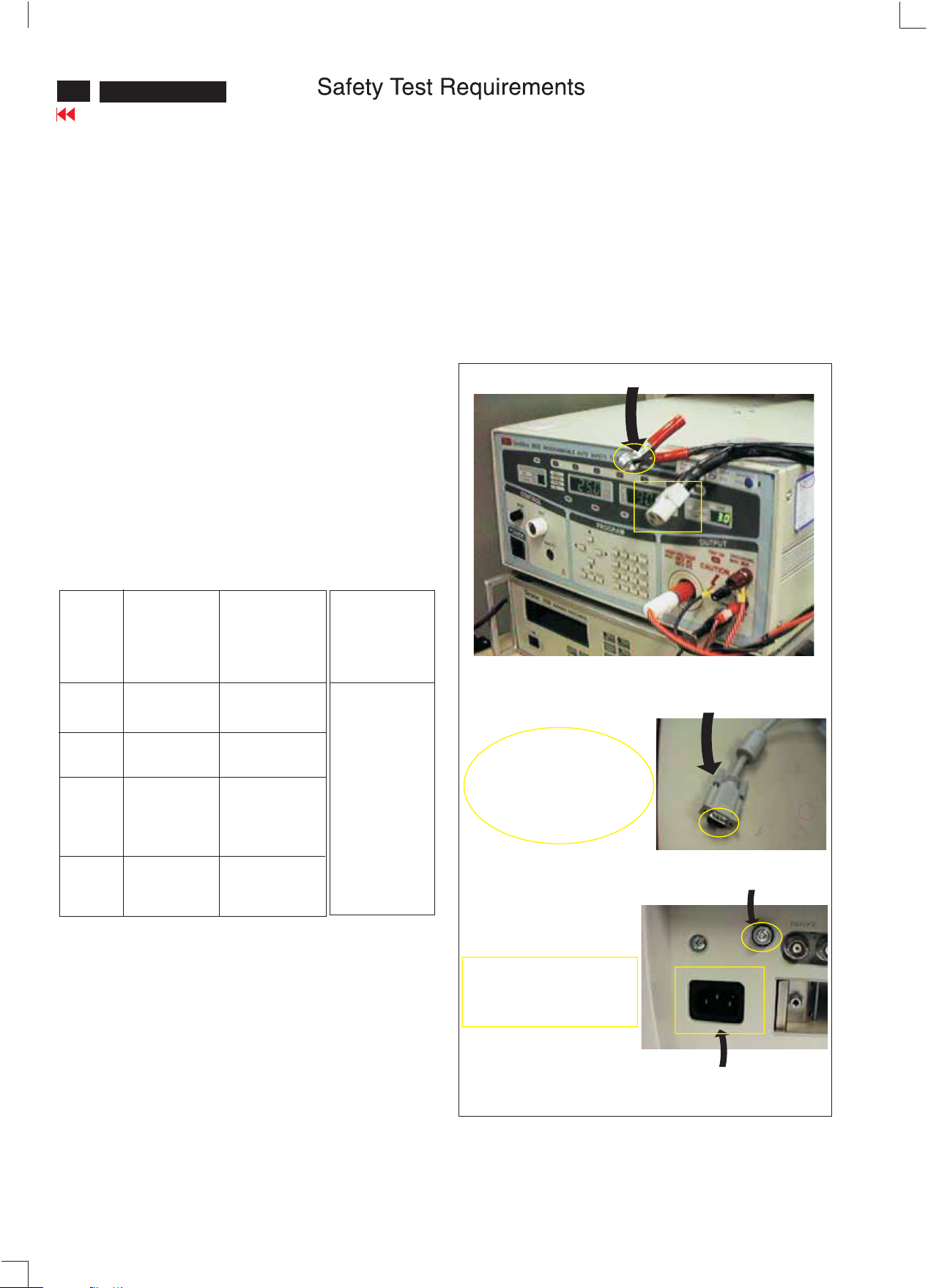
All units that are returned for service or repair must pass the
original manufactures safety tests. Safety testing requires both
and testing.Hipot Ground Continuity
HI-POT TEST INSTRUCTION
1.Application requirements
1.1 All mains operated products must pass the Hi-Pot test as
described in this instruction.
1.2 This test must be performed again after the covers have
been refitted following the repair, inspection or modification
of the product.
Test method
2.
2.1 Connecting conditions
2.1.1 The test specified must be applied between the parallel-
blade plug of the mainscord and all accessible metal
parts of the product.
2.1.2 Before carrying out the test, reliable conductive
connections must be ensured and thereafter be
maintained throughout the test period.
2.1.3 The mains switch(es) must be in the "ON" position.
2.2 Test Requirements
All products should be HiPot and Ground Continuity tested as
follows:
3. Equipments and Connection
3.1. Equipments
For example :
- ChenHwa 9032PROGRAMMABLE AUTO SAFETY
TESTER
- ChenHwa 510B Digital Grounding Continuity Tester
- ChenHwa 901 (AC Hi-pot test), 902 (AC, DC Hi-pot test)
Withstanding Tester
3.2. Connection
* Turn on the power switch of monitor before Hipot and
Ground Continuity testing.
Clip
Clip
Condition HiPot Test for HiPot Test for Ground Continuity
products where products where Test requirement
the mains input the mains input is
range is Full 110V AC(USA
range(or 220V type)
AC)
Test 2820VDC 1700VDC Test current:
voltage (2000VAC) (1200VAC) 25A,AC
Test time:
Test time 3 seconds 1 second 3 seconds(min.)
(min.) Resistance
required:
Trip set at 100 uA 5 mA <=0.09+Rohm,
current for Max. R is the
(Tester) limitation; set resistance of
at 0.1 uA for the mains cord.
Min. Limitation
Ramp set at 2
time seconds
(Tester)
2.2.1 The minimum test duration for Quality Control Inspector
must be 1 minute.
2.2.2 The test voltage must be maintained within the specified
voltage + 5%.
(ChenHwa 9032 tester)
Video cable
Connect the "video cable"
or "grounding screw"
to the CLIP on your tester.
Grounding screw
Connect the power cord
to the monitor.
2.2.3 There must be no breakdown during the test.
2.2.4 The grounding blade or pin of mains plug must be
conducted with accessible metal parts.
Power outlet
4. Recording
(Rear view of monitor)
Hipot and Ground Continuity testing records have to be kept
for a period of 10 years.
Page 23
HP L2025
HP L1740
HP L2025
HP L2025
Go to cover page
25
7
23
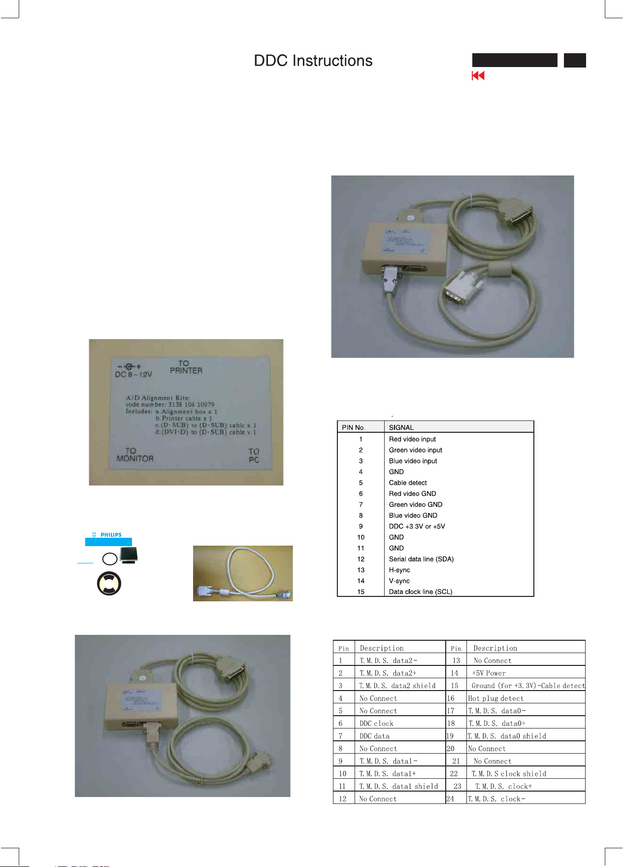
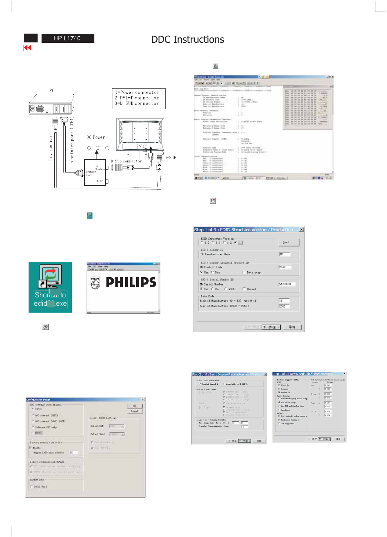
General
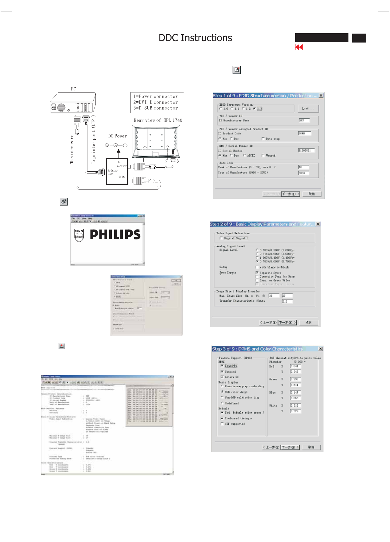
DDC Data Re-programming
In case the DDC data memory IC or main EEPROM which storage all
factory settings were replaced due to a defect, the serial numbers have
to be re-programmed" Analog DDC IC, Digital DDC IC & EEPROM".
It is advised to re-soldered DDC IC and main EEPROM from the old
board onto the new board if circuit board have been replaced, in this
case the DDC data does not need to be re-programmed.
Additional information
Additional information about DDC (Display Data Channel) may be
obtained from Video Electronics Standards Association (VESA).
Extended Display Identification Data(EDID) information may be also
obtained from VESA.
DDC EDID structure
For Analog interface: Standard Version 3.0
Structure Version 1.2
For Digital inferface: Standard Version 3.0
Structure Version 1.3
System and equipment requirements
1.Ani486 (or above) personal computer or compatible.
2. Microsoft operation system Windows 95/98.
3. EDID301.EXE program (3138 106 10103) as shown in Fig. 1
EDID 46 release.exe (in the cd-rom manual
4. A/D Alignment kits (3138 106 10079):
inclusion : a. Alignment box x1 (as Fig. 2)
Note: The alignment box has already build-in a batteries socket for
Using batteries (9V) as power source. Pull out the socket by
remove four screws at the rear of box. Please do not forget that
remove batteries after programming. The energy of batteries can
only drive circuits for a short period of time.
Fig.5
A/D Alignment Kits - Digital connection
b. Printer cable x1
c. (D-Sub) to (D-Sub) cable x1
d. (DVI-D) to (D-Sub) cable x1 (as Fig. 3)
Note: The EDID301.EXE (Release Version 1.58 20000818)is a
windows-based program, which cannot be run in MS-DOS.
i
n
o
M
U
C
B
s
c
i
n
Service
o
r
t
c
e
l
Service
E
r
e
Service
m
u
s
n
o
C
s
p
i
l
i
h
P
CD-ROM with EDID46.EXE
e
R
t
h
g
i
r
y
p
o
C
u
o
h
z
u
S
n
i
e
d
a
M
s
r
o
t
Service Manual
Fig.1
3
1
8
3
1
0
d
6
e
v
1
r
0
e
4
s
3
7
S
u
b
j
e
c
t
t
o
m
o
d
i
f
i
c
a
t
i
o
n
J
u
n
1
6
2
0
0
4
h
t
t
p
:
/
/
w
w
w
.
p
h
i
l
i
p
s
.
c
o
m
BCU Monitors
O
T
-
D
-
R
O
O
O
O
R
D
Oct28, 2004
3138106 10437
HPL1740LCD
E
E
X
C
C
I
H
V
A
R
N
E
G
S
E
Fig.3
(DVI-D) to (D-Sub) cable
Fig.2
Pin assignment
A. 15-pin D-Sub Connector
B. Input DVI -D Connector pin
Fig.4
Page 24
24
HP L1740
Go to cover page
Configuration and procedure
There are 2 chips contained OSD string, serial number..etc
on the circuit board, main EEPROM which storage all factory
settings,OSD string. DDC IC which storage 128byte EDID data(serial
number ..etc.). Following descirptions are the connection and procedure
for Analog and Digital DDC application, the main EEPROM can be
re-programmed along with Analog/Digital IC by enable factory memory
data write function on the DDC program (EDID301.EXE).
Initialize alignment box
In order to avoid that monitor entering power saving mode due
to sync will cut off by alignment box, it is necessary to initialize
alignment box before running programming software
(EDID301.EXE). Following steps show you the procedures and
writing block 4
connection.
Step 1: Supply 8~12V DC power source to the Alignment box by
plugging a DC power cord or using batteries.
Step 2: Connecting printer cable and video cable of monitor as Fig. 6
8-12v
+
4.6
edid46Release For
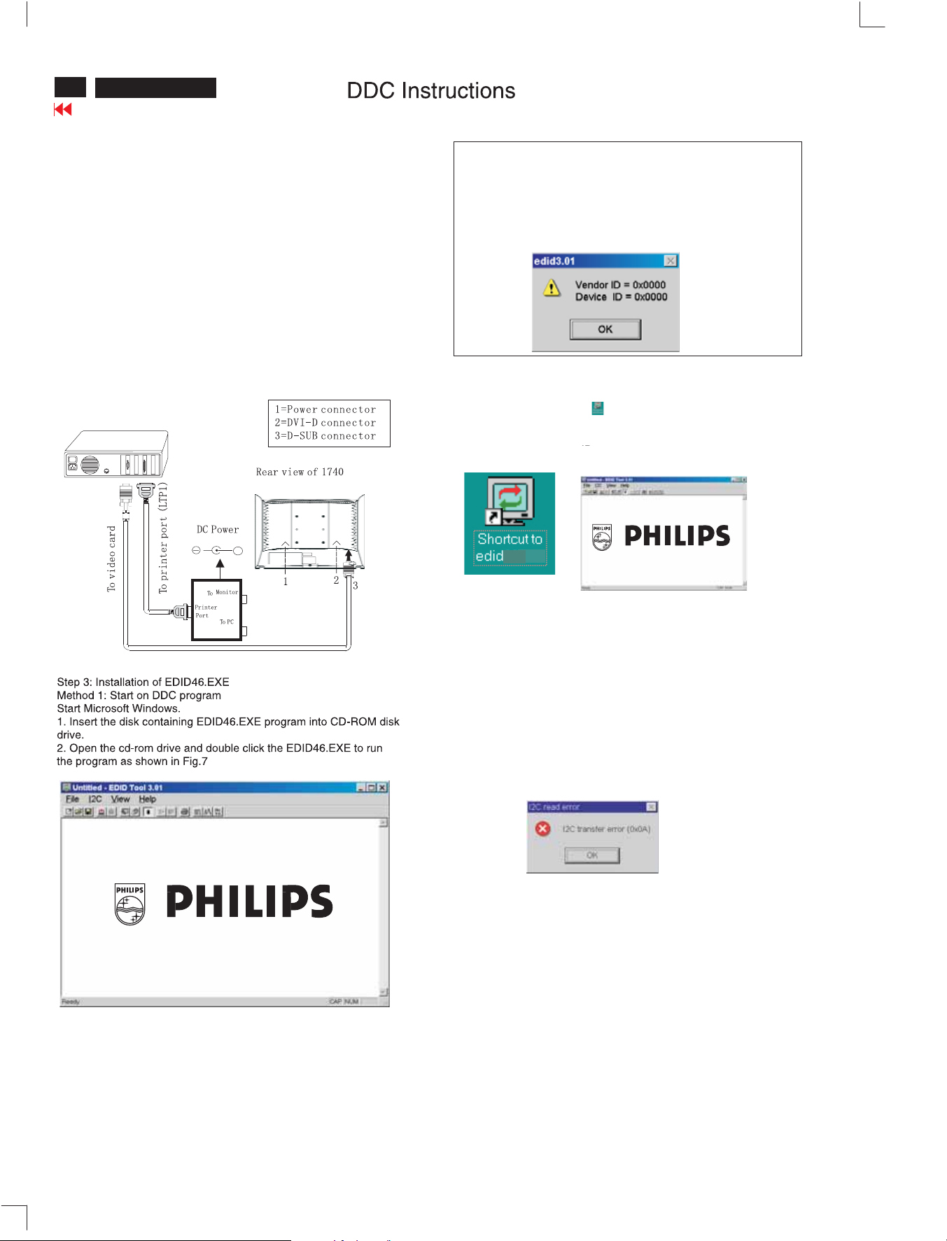
Note 1: If the connection is improper, you will see the following error
message (as shown in Fig. 8) before entering the main menu.
Meanwhile, the (read EDID) function will be disable. At this time,
please make sure all cables are connected correctly and fixedly,
and the procedure has been performed properly.
Fig.8
Method 2: After create a shortcut of EDID301.EXE
This is for initialize alignment box.
: Double click EDID301 icon
is on the screen of Windows Wallpaper.
Bring up main menu of EDID301 as shown in Fig. 10.
This is for initialize alignment box.
4.6
46
46
(as shown in Fig. 9) which
46
Fig.10
Fig.6
Fig.9
Note 2: During the loading, EDID301 will verify the EDID data which just
loaded from monitor before proceed any further function, once
the data structure of EDID can not be recognized, the following
error message will appear on the screen as below. Please
confirm following steps to avoid this message.
1. The data structure of EDID was incorrect.
2. DDC IC that you are trying to load data is empty.
3. Wrong communication channel has set at configuration setup
windows.
4. Cables loosed or poor contact of conn
46
ection.
Fig.7
You can copy the EDID46 to the hard disk and then execute
the program with the same steps as above
Page 25
HP L1740
HP L2025
HP L2025HP L2025
Go to cover page
25
7
25
Re-programming Analog DDC IC
Step 1: After initialize alignment box, connecting all cables and
box as shown in Fig. 14
8-12V
+
Fig/14
Step 2: Read DDC data from monitor
1. Click icon as shown in Fig. 15 from the tool bar to bring up
the Channels "Configuration Setup" windows as shown in Fig. 16.
Fig.15
Step 3: Modify DDC data (verify EDID version, week, year)
1. Click (new function) icon from the tool bar, bring up
Step 1 of 9 as shown in Fig. 18 .
4.6
EDID301 DDC application provides the function selection and
text change (select & fill out) from Step 1 to Step 9.
Fig.18
Step 4: Modify DDC data (Monitor Serial No.)
1. Click Next , bring up Fig. 19.
2. Select the DDC2B as the communication channel.
and "Enable Factory mode"
As shown in Fig. 16.
3. Click OK button to confirm your selection.
4. Click icon (Read EDID function) to read DDC EDID data from
monitor. The EDID codes will display on screen as shown in Fig. 17.
I
Fig.16
Fig.17
Fig.19
2. Click Next , bring up Fig. 20.
Fig.20
Page 26
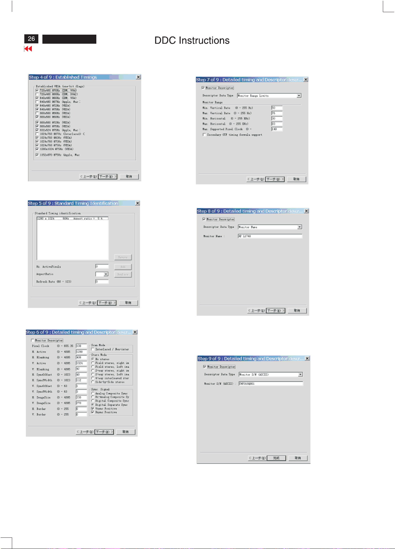
HP L1740
Go to cover page
3. Click Next , bring up Fig. 21.
4. Click Next , bring up Fig. 22
6. Click Next , bring up Fig. 24
Fig.24
Fig.21
7. Click Next , bring up Fig. 25
Fig.25
5. Click Next , bring up Fig. 23
Fig.22
8. Click Next , bring up Fig. 26.
- Serial number can be filled up or be changed at this moment.
- Click Finish to exit the Step window.
Fig.23
Fig.26
Page 27
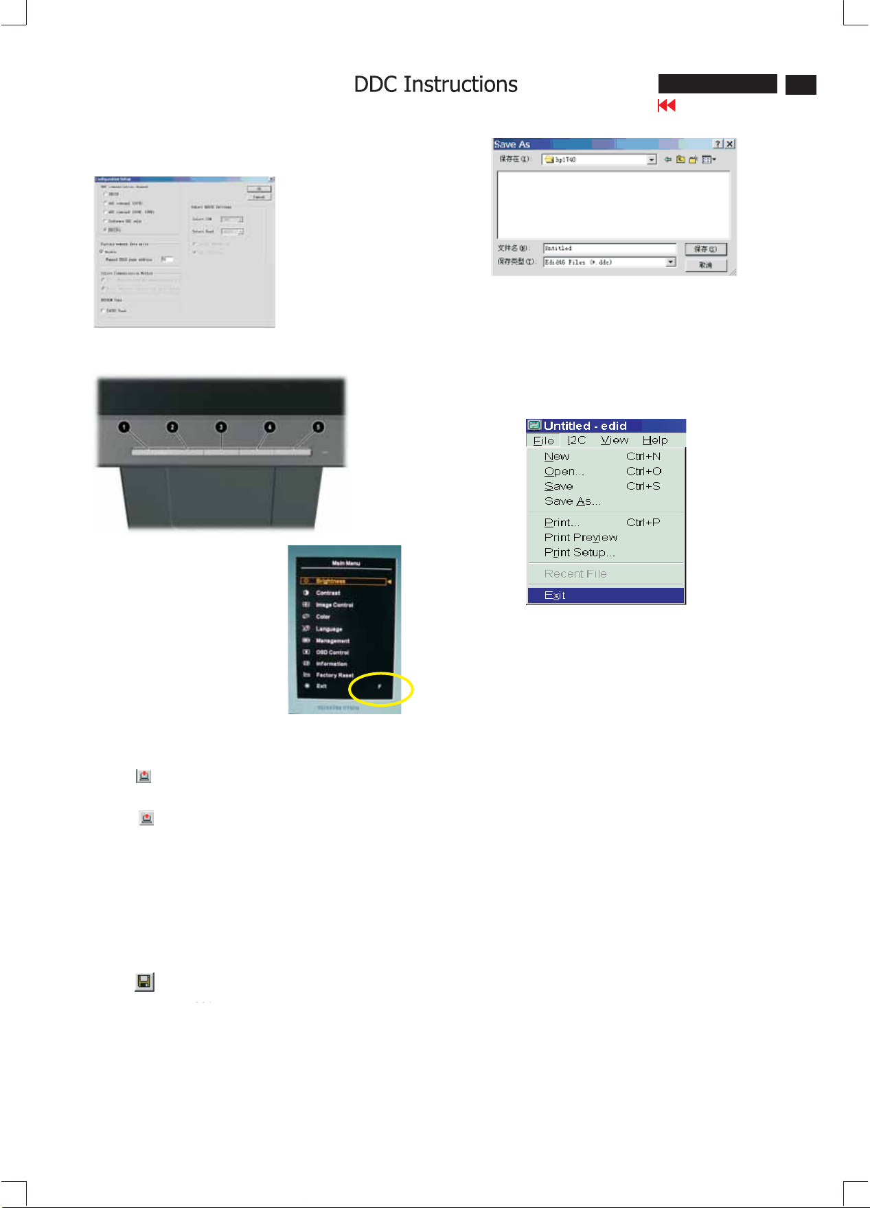
Step 5: Write DDC data
1. Configuration should be as Fig. 27.
HP L2025
HP L1740
HP L2025
HP L2025
Go to cover page
25
7
27
2.
Access Factory Mode
Power off on the monitor,
To hold Auto And
+ " + " buttons at the
same time ,
And press POWER
button to power on the monitor.
Press MANU button to
bring up OSD menu for
confirmation
" 1 "
" 4 "
Fig.27
1730
46
Fig.29
2. Click . Save
Step 8: Exit DDC program
Pull down the File menu and select Exit as shown in Fig. 30.
46
Fig.30
NOTE: If the run in
Edid46Release
Win 95/98with some problem, try to run it in win 2000,
but you should install the first.
EDID_PORT_TOOL
The other step is the same as described .above
3. Click (Write EDID) icon from the tool bar to write DDC data.
Bring up "Writing 0%~100%, ready" a progressing bar on the left
down corner.
4. Click (Read EDID) to confirm it.
5. You can confirm the S/N in the OSD also
press the menu and enter the management then you can see the
S/N.
Step 6: Save DDC data
Sometimes, you may need to save DDC data as a text file for using
in other IC chip. To save DDC data, follow the steps below:
1. Click (Save) icon (or click "file"-> "save as") from the tool bar
And give a file name as shown in Fig. 29.
The file type is EDID301 file (*.ddc) which can be open in WordPad.
By using WordPad, the texts of DDC data & table (128 bytes, hex
code) can be modified. If DDC TEXTS & HEX Table are completely
correct, it can be saved as .ddc flie to re-load it into DDC IC for DDC
Data application.
4.6
Page 28
28
Go to cover page
Re-programming Digital DDC IC
Step 1:Connecting all cables and alignment box as shown in
Fig. 31.
8-12
+
Fig.31
Step 2: Initialize alignment box
(Shortcut of EDID301.EXE on Windows Wallpaper already.)
Double click EDID301 icon (as shown in Fig. 32) which is
on the screen of Windows Wallpaper.
Bring up main menu of EDID301 as shown in Fig. 33.
4.6
4.6
4.6
4. Click icon (Read EDID function) to read DDC EDID data from
monitor. The EDID codes will display on screen as shown in Fig. 35.
Fig.35
Step 4: Modify DDC data (verify EDID version, week, year)
1. Click (new function) icon from the tool bar, bring up
Step 1 of 9 (Digital) as shown in Fig. 36 .
EDID4.6 DDC application provides the function selection and
text change (select & fill out) from Step 1 to Step 9.
Fig.32
4.6
Step 3: Read DDC data frommonitor
1. Click icon from the tool bar to bring up the Channels
Configuration Setup windows as shown in Fig. 34.
2. Select the DDC2B as the communication channel.
and "Enable Factory mode"
3. Click OK button to confirm your selection.
I
Fig.34
Fig.33
Fig.37
Fig.36
Fig.38
Page 29

Fig.39
Fig.40
HP L1740
HP L2025
HP L2025
HP L2025
Go to cover page
Step 6: Write DDC data
1. Click (Write EDID) icon from the tool bar to write DDC data.
2. Click (Read EDID) to re-confirm (check contents) it.
The 128bytes DDC data which had been written into DDC IC of
Digital Mode.
Step 7: Save DDC data
Sometimes, you may need to save DDC data as a text file for using
in other IC chip. To save DDC data, follow the steps below:
1. Click (Save) icon (or click "file"-> "save as") from the tool bar
and give a file name as shown in Fig. 45.
2. Click . Save
25
7
29
Fig.41
R
Fig.43
Step 5: Modify DDC data (Monitor Serial No.)
Monitor serial No. can be filled up or be changed as shown in Fig. 44
Click Finish to exit the Step window
Fig.42
Fig.44
R
Step 8: Load DDC data
1. Click from the tool bar.
2. Select the file you want to open as shown in Fig 46.
3. Click Open
R
Step 9: Exit DDC program
Pull down the File menu and select Exit
NOTE: If the run in
Edid46Release
Win 95/98with some problem, try to run it in win 2000,
but you should install the first.
EDID_PORT_TOOL
The other step is the same as described .above
Page 30

30
HP L1740
Go to cover page
DDC Data
THEDISPL AY DATA CHANNEL (DDC_2B ) CONTENT INCLUDING
(FOR HP L1740 ANALOG)
**********************************************************************
EDID log file
**********************************************************************
Vendor/Product Identification
ID Manufacturer Name : HWP
ID Product Code : 2648(HEX.)
ID Serial Numb er : 1010101 (HEX.)
Week of Manufacture : 36
Year of Manufacture : 2004
EDID Version, Revision
Version : 1
Revi sio n : 3
Basic Display Paramet ers/Featu res
Video Input Definition : Analog Video Input
0.700V/0.000V(0.70Vpp)
without Blank-to-Black Setup
Separate Sync
without Composite Sync
without Sync on Green
no Serration required
Maximu m H Image Size : 33
Maximum V Image Size : 27
Display Transfer Characteristic : 2.2
(gamma)
Feature Suppor t (DPMS) : St andby
Suspend
Active Off
Display Type : RGB color display
Standard Default Color Space : Primary color space
Preferred Timing Mode : Detailed timing block 1
Color Characteristics
Red X coordinate : 0.641
Red Y coordinate : 0.342
Green X coordinate : 0.292
Green Y coordinate : 0.611
Blue X coordinate : 0.147
Blue Y coordinate :
White X coordinate : 0.313
White Y coordinate : 0.329
Established Timings
Established Timings I : 720 x 400 @70Hz(IBM,VGA)
Established Timings II : 800 x600 @72Hz (VESA)
Manufacturer's timings : 1152x870 @75Hz (Apple,Mac II)
Standard Timing Identification #1
Horizontal active pixels : 1280
Aspect Ratio : 5:4
0.068
640 x 480 @60Hz(IBM,VGA)
640 x 480 @72Hz (VESA)
640 x 480 @75Hz (VESA)
800 x600 @60Hz (VESA)
800 x600 @75Hz (VESA)
832x624 @75Hz (Apple,Mac II)
1024 x 768 @60Hz (VESA)
1024 x 768 @
1024 x 768 @75Hz (VESA)
1280 x 1024 @75Hz (VESA)
70Hz (VESA)
Refresh Rate : 60
Detailed Timing #1
Pixel Clock (MHz) : 108
H Active (pixels) : 1280
H Blanking (pixels) : 408
V Active (lines) : 1024
V Blanking (lines) : 42
H Sync Offset (F Porch) (pixels): 48
H Sync Pulse Width (pixels) : 112
V Sync Offset (F Porch) (lines) : 1
V Sync Pulse Width (lines) : 3
H Image Size (mm) : 338
V Image Size (mm) : 270
H Border (pixels) : 0
V Border (lines) : 0
Flags : Non -interlaced
: Normal Display, No stereo
: Digital Separate sync.
: Positive Vertical Sync.
: Positive Horizontal Sync.
Monitor Descriptor #2
Monitor Range Lim its
Min. Vt rate Hz:50
Max. Vt rate Hz:76
Min. Horiz. rate kHz:30
Max. Horiz. rate kHz:83
Max. Supported Pixel : 140
No secondary GTF timing formula supported.
Monitor Descriptor #3
Monitor Name : HP L1740
Monitor Descriptor #4
Serial Number : CN
Extension Flag : 0
Check sum : 96 (HEX.)
**********************************************************************
EDID data (128 bytes)
**********************************************************************
0: 00 1:ff 2:ff 3:ff 4:ff 5:ff 6:ff 7: 00
8: 22 9: f010: 48 11 :26 12: 01 13: 01 14: 01 15: 01
16: 2 417: 0e 18: 01 19: 03 20:68 21:21 22: 1b23: 78
24: ee 25: 2e 26: e5 27:a4 28: 57 29: 4a 30:9c 31:25
32: 11 3 3 :5034:5435: ad 36: ef 37:8038: 8139: 80
40: 01 41:
48: 01 49: 01 50: 01 51: 01 52: 01 53: 01 54: 30 55: 2a
56: 00 57: 98 58: 51 59: 00 60:2a 61: 40 62: 30 63: 70
64: 13 65: 00 66: 52 67: 0e 68: 11 69: 00 70: 00 71: 1e
72: 00 73: 00 74: 00 75: fd 76: 00 77: 32 78: 4c 79: 1e
80:5
88: 20 89: 20 90: 00 91: 00 92: 00 93:fc 94: 00 95: 48
96: 50 97:20 98: 4c 99: 31 100: 37 101: 34 102: 30 103: 0a
104:20105: 20106: 20 107:20108: 00 109: 00 110: 00 111 :ff
112: 00 113: 43 114: 4e 11 5: 50116: 34 117: 33 118: 30 119: 58
0: 30 121: 30 122: 31 123: 0a 124:20125: 20126: 00 127:96
12
01 42: 01 43: 01 44: 01 45: 01 46: 01 47: 01
3 81: 0e 82: 00 83: 0a84:20 85: 20 86: 20 87:20
P430X001
Page 31

DDC Data
HP L1740
Go to cover page
31
(FOR HP L1740 Digital)
**********************************************************************
EDID log file
**********************************************************************
Vendor/Product Identification
ID Manufacturer Name : HP
ID Product Code : 2649 (HEX.)
ID Serial Number : 1010101 (HEX.)
Week of Manufacture : 36
Year of Manufacture : 2004
EDID Version, Revision
Version : 1
Revision : 3
Basic Display Parameters/Features
Video Input Definition : Digital Video Input
Maximum H Image Size : 33
Maximum V Image Size : 27
Display Transfer Characteristic : 2.2
(gamma)
Feature Support (DPMS) : Standby
Suspend
Active Off
Display Type : RGB color display
Standard Default Color Space : Primary color space
Preferred Timing Mode : Detailed timing block 1
Color Characteristics
Red X coordinate : 0.641
Red Y coordinate : 0.342
Green X coordinate : 0.292
Green Y coordinate : 0.611
Blue X coordinate : 0.147
Blue Y coordinate : 0.068
White X coo rdinate : 0.313
White Y coordinate : 0.329
Established Timings
Established Timings I : 720 x 400 @70Hz (IBM,VGA)
640 x 480 @60Hz (IBM,VGA)
640 x 480 @72Hz (VESA)
640 x 480 @75Hz (VESA)
800 x 600 @60Hz (VESA)
Established Timings II : 800 x 600 @72Hz (VESA)
800 x 600 @75Hz (VESA)
832 x 624 @75Hz (Apple,Mac II)
1024 x 768 @60Hz (VESA)
1024 x 768 @70Hz (VESA)
1024 x 768 @75Hz (VESA)
1280 x 1024 @75Hz (VESA)
Manufacturer's timings : 1152 x 870 @75Hz (Apple,Mac II)
Standard Timing Identification #1
Horizontal active pixels : 1280
Aspect Ratio : 5:4
Refresh Rate : 60
Detailed Timing #1
Pixel Clock (MHz) : 108
H Active (pixels) : 1280
H Blanking (pixels) : 408
V Active (lines) : 1024
V Blanking (lines) : 42
H Sync Offset (F Porch) (pixe ls): 48
H Sync Pulse Width (pixels) : 11 2
V Sync Offset (F Porch) (lines) : 1
V Sync Pulse Width (lines) : 3
H Image Size (mm) : 338
V Image Size (mm) : 270
H Border (pixels) : 0
V Border (li nes) : 0
Flags : Non -interlaced
: Normal Display, No stereo
: Digital Separate sync.
: Positive Vertical Sync.
: Positive Horizontal Sync.
Monitor Descriptor #2
Monitor Range Limits
Min. Vt rate Hz : 50
Max. Vt rate Hz : 76
Min. Horiz. rate kHz : 30
Max. Horiz. rate kHz : 83
Max. Supported Pixel : 140
No secondary GTF timing formula supported.
Monitor Descriptor #3
Monitor Name : HP L1740
Monitor Descriptor #4
Serial Number : CNP430X001
Extension Flag : 0
Check sum : 6D (HEX.)
**********************************************************************
EDID data (128 bytes)
**********************************************************************
0: 00 1:ff 2:ff 3:ff 4:ff 5:ff 6:ff 7:00
8: 22 9: 00 10: 49 11:26 12: 0113:0114: 0115: 0 1
16: 24 17: 0e 18: 0119: 03 20: 80 21:21 22: 1b23:78
24: ee 25: 2e 26: e5 27: a4 28: 57 29: 4a 30: 9c 31:25
32: 11 3 3 :50 34: 54 35: ad 36: ef 37: 80 38: 8139: 80
41:01 42: 01 43:01 44: 01 45: 01 46: 01 47: 0 1
40: 01
48: 01 49: 01 50: 01 51:01 52: 01 53:01 54: 30 55: 2a
56: 00 57: 98 58: 51 59: 00 60: 2a 61:40 62:3063:70
64: 13 65: 00 66: 52 67: 0e 68: 11 69: 00 70: 00 71: 1e
72: 00 73: 00 74: 00 75: fd 76: 00 77: 32 78: 4c 79: 1 e
80: 53 81: 0e 82: 00 83: 0a 84: 20 85: 20 86: 20 87: 20
88: 20 89: 20 90: 00 91: 00 92: 00 93: fc 94: 00 95: 48
96: 50 97: 20 98: 4c 99: 31 100: 37 101: 34 102: 30 103:0a
104: 20 105: 20 106: 20 1 07: 20
112: 00 11 3 :43114: 4e 11 5: 50 116: 34 117: 33 118: 30 119: 58
120: 30 121: 30 122: 31 123:0a124: 20 125: 20 126: 00 127: 6d
108: 00 109: 00 110: 00 111:ff
1
1
e
Page 32

32
HP L1740
ISP CABLE for CPU
Go to cover page
Configuration and procedure
ISP ( In System Program) software is provided by Genesis to upgrade
the firmware of CPU.
ISP cable is for the interface between "Parallel port of PC" and
"15 pin-D-SUB connector of monitor.
System and equipment requirements:
1. An i386 (or above ) personal computer or compatible.
2. Microsoft operation system Win 95/98 or Win 2000
3. ISP software
4. ISP cable (3138 106 10213) as shown in Fig.1
Fig.4
Step 5 . Click the next till the setup finished. And creat a short cut on the desktop.
Fig.1 ISP CABLE :12NC IS "3138 106 10213".
5.Connect ISP cable and main cord to monitor as shown in Fig.2.
6. Install and setup the Gprobe 4.5.0.5.exe program
step 1. Create a folder in your PC .for example: D:\1740
step 2.Copy ISP software 1740 software .Zip into your folder
step 3.Unzip ISP.ZIP into your folder as shown in Fig.3
step 4.Double click the Gprobe4.5.0.5.exe icon to install the
application as shown Fig.4
Fig.3
Page 33

Update the firmware
1. Double click the Gprobe.exe icon ,then appears window
as shown in Fig.5
2. Press the options then choose configure Pin as shown in Fig.5
3. From the menu that appears, choose the number 17 in "output
pin and the number 12 in " input pin as shown in Fig.6
Fig.5
Fig.6
Go to cover page
Fig.8
Update the firmware
click the commands and select the Batch, as
shown in Fig.9, Fig.10
4. Press the options then choose connection setup as shown in
Fig.7
5. From the menu that appears , choose the DDC2Bi3 in "protocol"
and the LPT (0x378) in "port" as shown in Fig.8
Fig.7
Fig.9
Fig.10
ClickthebuttonasshowninFig.10tobrowsetheIicisp.txt fileinthe
folder that you create.
Note: you should pay attention to the path in the Iicisp.txt file.
It is the same as the folder's path that you create.
Page 34

34
HP L1740
Go to cover page
Fig.11 click "OPEN"
ISP CABLE FOR CPU
Shut of the AC power
Click the "OK" button and then open the AC power, after the follow
window appears, the update is completed.
Page 35

Repair Tips
HP L2025
HP L2025HP L2025
HP L1740
Go to cover page
25
7
35
0.Warning
All ICsand many other semi-conductors are susceptible to
electrostaticdischarges (ESD). Careless handling during
repair can reduce life drastically. When repairing, makesure
that you are connectedwith thesamepotential as the mass
of the un
and toolsalso atthesamepotential!
itvia a wristwrap with resistance.Keep components
1.Servicing of SMDs (Surface MountedDevices)
1.1 Generalcautions on handling and storage
-Oxidation on the terminals of SMDsresultsin poorsoldering.
Do not handle SMDs with bare hands.
-Avoidusing storageplaces that are sensitive to oxidation
such as places with sulphur or chlorine gas,direct sunl
high temperatures orahigh degree of humidity. The
capacitance or resistance value of the SMDs maybe
affectedbythis.
- Rough handling of circuitboards containing SMDs may
cause damage to the componentsas
well as the circuit
boards.Circuitboards containing SMDsshould never be
bent or flexed. Different circuitboardmaterialsexpand and
contract atdifferent rates whenheatedor cooled and the
componentsand/orsolder conn
ections maybe damaged
due to thestress.Never rub orscrape chip componentsas
this maycause the value of the component to change.
Similarly,donotslide the circuitboard across any surface.
1.2 RemovalofSMDs
- Heatthesolder (for 2-3seconds) at each terminalofthe
chip.Bymeans of litz wire and aslight horizontalforce,
small components canberemovedwith thesoldering iron.
Theycan alsoberemovedwith asolder sucker (see Fig.
1A)
ight,
preferably beequippedwith a thermal control (soldering
temperature:225 to 250 C).
- The chip, onceremoved, mustnever bereused.
1.4 Attachment of SMDs
- Locate the SMD on thesolder lands by means of tweezers
and solder the component on oneside.Ensure thatthe
component is positionedcorrectly on thesolder lands (see Fig.2A).
-Next complete thesoldering of the terminals of the
component (see Fiq. 2B).
2. Caution when attaching SMDs
-When soldering the SMD terminals, do not touch them
directly with thesoldering iron. Thesoldering should be
doneasquickly as possible,care mustbe takentoavoid
damage to the terminals of the SMDs themselves.
-Keep the SMD's body in conta
soldering.
- Thesoldering iron to be used(approx. 30 W)should
preferably beequippedwith a thermal control (soldering
temperature:225 to 250 C).
- Soldering should not be done outside thesolder land.
- Soldering flux (of rosin) maybe used, but should not b
acidic.
- After soldering, letthe SMD cool down gradually at room
temperature.
- The quantity of solder mustbeproportionaltothesize of the
solder land. If the quantity is too great, the SMD might
crack or thesolder lands might be torn loose
printedboard(see Fig. 3).
ct with the printedboardwhen
e
from the
While holding the SMD with a pair of tweezers,takeitoffgently using the
soldering iron's heat appliedtoeach terminal(see Fig. 1 B).
- Remove theexcess solder on thesolder lands by means of
litz wire orasolder sucker (see Fig. 1C).
1.3 Caution on removal
-Whenhandling thesoldering.iron. use suitable pressure a nd be careful.
-When removing the chip, do not use undue force with the pair of tweezers.
- Thesoldering iron to be used(approx. 30 W) should
Right
Fig.3 Examples
Page 36

36
HP L1740
Go to cover page
Repair Flow Chart
AC IN
Power Board
21
X
Control Board
Scaler Board
LCD Panel
No power
(power indicator off)
Check 12V/5V/3.3V
NG
Gnd
2
Bad power board
12v
Connector 1102
3.3v
7
10
5.0v
14
Bad Scaler Board
NG
OK
Check Scaler Board
OK
Check Control Board
OK
Check LCD Panel
3.3v
5.0v
Gnd
Connector1503
Check Control Wires
Page 37

Repair Flow Chart
HP L1740
Go to cover page
37
Power board
Bad Power
Board
Check scaler board
Page 38

38
HP L1740
Go to cover page
Repair Flow Chart
21
X
Power board
Check LCD Panel
Control board
Check scaler board
Page 39

Wiring Diagram
HPL1740
Go to cover page
39
Page 40

40
HP L1740
Go to cover page
Block Diagram
Control
Board
Downstream
port x2
Upstream
port
DVI
EEPROM
5V
D2+/D2-
D1+/D1-
USB 2.0
GL 850
D0+/D0-
5V
R+-/G+-/B+-/CLK+-
Key Function
3.3V
R+-/G+-/B+-/CLK+R/G/B
Schmitter
HS/VS
DSUB_CA
ISPSCL,SDA
DDC
gate
Write_enable
Scaler
Gm5321
RXEC+/-
30 Pin Connector to panel
RXE3+/RXE2+/-
AC to DC
Power
+Inverter
Board
Flash
Memory
D-SUB
R/G/B
BL_EN, Brightness
5V
3.3V
ADDR0/17, Data 0/7
Bank, ROM_OE/WE,
Panel_ID
EEPROM
3.3V
IIC
1.8V
Reg.
Power Control
LVDS
Panel PWR
MOS
RXE1+/RXE0+/-
RXOC+/RXO3+/-
RXO2+/-
RXO1+/RXO0+/-
5V for LPL/CPT
12V
Page 41

HP L1740
Go to cover page
41
Page 42

42
HP L1740
Go to cover page
Page 43

Scaler Diagram-3
HP L1740
Go to cover page
41
Page 44

44
HP L1740
Go to cover page
Page 45

Scaler Diagram-5
HP L1740
Go to cover page
45
Page 46

46
HP L1740
Go to cover page
Page 47

HP L1740
Go to cover page
47
Page 48

48
HP L1740
Go to cover page
Page 49

AC/DCSchematic
Power Diagram-1
HP L1740
Go to cover page
49
Page 50

50
Go to cover page
HP L1740
Inverter Schematic
Power Diagram-2
Page 51

AC/DCFunctionBlockSchematic
Power Diagram-3
HP L1740
Go to cover page
51
Page 52

52
Go to cover page
HP L1740
Inverter FunctionBlockSchematic
Power Diagram-4
Page 53

Power Diagram-5
HP L1740
Go to cover page
53
Bottom layer
Bottom SilkScreenOverlayer
Page 54

54
Go to cover page
Bottom Silk ScreenOverlayer
HP L1740
Power Diagram-6
Page 55

41
313815414631
Exploded View
BACK COVER
HP L1740
50
55
313815861521
1051
313815861641
SCALER ASSY-AUO
STAND-HPL1740
313815758191
SCALER ASSY-CPT
LIP S(T50P062.00)
823827716311
1052
313815861601
MAIN FRAME+WIRE ASSY
HOUSING COVER
313810440571
100
1160
1050
932221491682
TFT-LCD M170EG01-V1 (AUOP)B
823827716231
30
LCD CLAA170EA07
313815758241
FRONT BEZEL ASSY
Page 56

56
HP L1740
Go to cover page
Model: HPL 1740
0030 313815758241 FRONT BEZEL ASSY
0041 313815414631 BACK COVER
0050 313815758191 STAND-HPL1740
0092 313815565791 FRONT COVER
0451 313815638711 CUSHION-R
0452313815638721 CUSHION-L
0453313815639141 P.E. BAG(EPE)
0456 313815639061 BASE P.E. BAG
0615 313811708001 HEX CODE OF F/W(NO MATL REQ)
8161 313819874271 CBLE-017 7/360/7-017 AWG28
7202 932216972682 IC SM AT24C02N-10SC-2.7(ATME)L
7203 932216972682 IC SM AT24C02N-10SC-2.7(ATME)L
7210 935260739118ICSM 74LVC14APW(PHSE) R
7301 313815861531 CPU IC ASSY
7301 932219386682 IC SMM29W022BT55K1 (ST00) L
73023
7302 932214725682 IC M24C16-WBN6 (ST00) L
7401 932220818671 IC SM GM5321-BC (GEMI) Y
7403 932220099685 IC SMLD1117 AS18 (ST00)R
7501 932200429685 TRA SIG SM BC857C (ONSE) R
7502 932200429685 TRA SIG SM BC857C (ONSE) R
7503 932209265685 TRA SIG SMMUN2211 J (ONSE) R
7504 932216638
7505 932219076668ICSML5972D (ST00)R
7601 823827716201 USB CONTROLLER
7608313815861571 EEPROM ASSY-USB
7608 823827716241 MEMORY IC
13815861541 EEPROM ASSY-AUO
668 FET POW SM SI5441DC (VISH)R
6201 933215370215 DIO SIG SM BAV99 (PHSE) R
6202 933215370215 DIO SIG SM BAV99 (PHSE) R
6203 933215370215 DIO SIG SM BAV99 (PHSE) R
6204 933215370215 DIO SIG SM BAV99 (PHSE) R
6205 933215370215 DIO SIG SM BAV99 (PHSE) R
6206 933215370215 DIO SIG SM BAV99 (PHSE) R
6207 933215370215 DIO SIG SM BAV99 (PHSE) R
620
8 933215370215 DIO SIG SM BAV99 (PHSE) R
6209 933137390215 DIO REG SM BZX84-C5V1 (PHSE) R
6220 933742280215 DIO SIG SM BAT54 (PHSE) R
6221 933913910115 DIO SIG SM BAS32L (PHSE) R
6222 933913910115 DIO SIG SM BAS32L (PHSE) R
6223 933742280215 DIO SIG SM BAT54 (PHSE) R
6501 932216670682 DIO REC SB240 A (VISH)B
Page 57

HP L1740
57
Model: HP L1740(AUO Panel)
Type:CJ6B50/76
Mechanical Parts
0030 313815758241 FRONTBEZELASSY
0041 313815414631 BACK COVER
0050 313815758191 STA ND-HPL1740
0092 313815565791 FRO NTCOVER
0100 313810440571 HOUSING COVER
1160 313815861601 MAIN FRAME+WIRE ASSY
LCD Panel
1050 932221491682 TFT-LCD M170EG01-V1 (AUOP) B
packing
0450 313815638701 CARTON
0451 313815638711 CUSH ION-R
04523138156387 21CUSHION-L
0453313815639141 P.E. BAG (EPE )
0456 313815639061 BASE P.E. BAG
PCB ASSY
1052 823827716311 L IPS(T50P062.00)
10533138158 60161 CONTROL ASSY
1051 313815861521 SCALER
Accessory
0601 313811707601 HP CD-ROM INF.
1157 31381 28749 01 MAINSCORD
8161 31 381 9874271 CBLE-017 7/360/7- 017 AWG28
816331 3819873971 FFC 30/180/301.0
Miscellanea
115 831381987143 1CORD SUB-D 15/1M8/15 D-SUB BK
115 931381987 3991CORD USBA/
1201 242203300521 S OC DVI H 24P F 1.91DVI-D Y
1203242202 518065 SOC SUBD H15PF BU 9 00 Y
1302243803 100435 SOC IC V8P F2.54 DILL
1410 242254300999 RES XTL SM14M31820P SM D-49R
141224220 2518682 CO
1601 242254301447 RES XTL SM12MHZ32P SMD-49R
1602 823827716661 USBBTYPERECE PTACLE CONN
1603 823827716671 USBA TYPEDOUBLE PORTCONN
160824380 3100435 S OC IC V8P F2.54 DILL
0291 313815565821 LABEL-CPU
0615 313811708001 HEX
0295 313815565831 LABEL-EEPR OM-AUO
0298 313815565841 LABEL-EEPROM- USB
4444 313810610438 service manual
4444 313810610437CD-Romservice manual
PCB ASSY
1051 313815861521 SCALER ASSY-AUO
2607 223878615649 CER2 0603X7R 16V 100N PM10 R
2608 223878615649 CER2 0603X7R 16V 100N PM10 R
2
609 223878615649 C ER2 0603X7R 16V 100N PM10 R
2610 223878615649 CER2 0603X7R 16V 100N PM10 R
2611 223878615649 CER2 0603X7R 16V 100N PM10 R
2612 223878615649 CER2 0603X7R 16V 100N PM10 R
2615 223878615649 CER2 0603X7R 16V 100N PM10 R
2616 20 2 002
2618 223878615649 CER2 0603X7R 16V 100N PM10 R
2619 223878615649 CER2 0603X7R 16V 100N PM10 R
2620 223886715189 CER10603NP0 50V 18P PM5 R
2621 223886715189 CER10603NP0 50V 18P PM5 R
2622 20 220 3100227 ELCAP K
2623 22387 8 615649 CER2 0603X7 R 16V 100N PM10 R
2624 202203100227 ELCAP K M 25VS100U PM20B
2625 223878615649 CER2 0603X7R 16V 100N PM10 R
2627 222224119876 CER2 1206 Y5V 10V 10U P80 20 R
2630 223878615649
2437 2020021 91725 E LCAP SM RVS 16V 10U PM20 R
2438 22387 8 615649 CER2 0603X7 R 16V 100N PM10 R
2439 20 2 00219172 5 ELCAP SM RVS 16V 10U PM20 R
2440 223878615649 CER2 0603X7R 16V 100N PM10 R
2441 2238
2442 223878615649 CER2 0603X7R 16V 100N PM10 R
2443 223878615649 CER2 0603X7R 16V 100N PM10 R
2444 223878615649 CER2 0603X7R 16V 100N PM10 R
2445 223878615649 CER2 0603X7R 16V 100N PM10 R
2446 223878615649 CER2
2450 223886715478 CER10603NP0 50V 4P7 PM0P25 R
2451 223886715478 CER10603NP0 50V 4P7 PM0P25 R
2452 223858615636CER2 0603X7 R 50V 10N PM10 R
2453 223858615636CER2 0603X7 R 50V 10N PM10 R
2454 223858615636CER2 0603X7 R 50V 10N PM10 R
2455 22385
2460 20 2 00219172 5 ELCAP SM RVS 16V 10U PM20 R
191725 E LCAP SM RVS 16V 10U PM20 R
78615649 CER2 0603X7R 16V 100N PM10 R
8615636CER2 0603X7R 50V 10N PM10 R
ASSY-AUO
2M/USBBBK
N H 30P F 1.00 S M FFC0.3 R
CODE OFF/W(NOMATLREQ)
M 25VS100U PM20B
CER2 0603X7R 16V 100N PM10 R
0603X7R 16V 100N PM10 R
2461 223878615649 CER2 0603X7R 16V 100N PM10 R
2501 223891015649 CER2 0805 X7R25V 100N PM10 R
2502 223891015649 CER2 0805 X7R25V 100N PM10 R
250320 2203100206 E LCAP SMHV25V 47U PM20 R
2504 223878615649 CER2 0603X7R 16V 100N PM10 R
2505 223878615649 CER2 0603X7R 16V 100N PM10 R
2506 20 220 3100206 ELCAP S MHV25V 47U PM20 R
2507 223878615649 CER2 0603X7R 16V 100N PM10 R
250
8 223878615649 C ER2 0603X7R 16V 100N PM10 R
250920 2203100206 E LCAP SMHV25V 47U PM20 R
2510 223878615649 CER2 0603X7R 16V 100N PM10 R
2511 223878615649 CER2 0603X7R 16V 100N PM10 R
2513 223878615649 CER2 0603X7R 16V 100N PM10 R
2515 20 380
2516 20 220 3100179ELCAP S MHV25V 10U PM20 R
2517 223858015641 CER2 0805 X7R 50V22NPM10 R
2518 223886715221CER10603NP0 50V220P PM5 R
251920 2203100068ELCAP GL 25VS470U PM2 0B
2520 223891015649 CER2 0805 X7R25V 100N PM10
2521 223878615649 CER2 0603X7R 16V 100N PM10 R
2523 22387 8 615649 CER2 0603X7 R 16V 100N PM10 R
2525 223878615649 CER2 0603X7R 16V 100N PM10 R
2529 22387 8 615649 CER2 0603X7 R 16V 100N PM10 R
2531 223878615649 CER2 0603X7R 16V 100N PM10
2601 223824619863 C ER2 0603Y5V 10V 1U P802 0 R
2602 223824619863 C ER2 0603Y5V 10V 1U P802 0 R
2603 223878615649 CER2 0603X7R 16V 100N PM10 R
2604 223878615649 CER2 0603X7R 16V 100N PM10 R
2605 223878615649 CER2 0603X7R 16V 100N PM10 R
2
606 223878615649 C ER2 0603X7R 16V 100N PM10 R
2201 223878615649 C ER2 0603X7R 16V 100N PM10 R
2202 223878615649 CER2 0603X7R 16V 100N PM10 R
2203 223878615649 CER2 0603X7R 16V 100N PM10 R
2204 223878615649 C ER2 0603X7R 16V 100N PM10 R
2209 223878615649
2214 223878615649 C ER2 0603X7R 16V 100N PM10 R
2219 223886715221CER10603NP0 50V220P PM5 R
2220 223878615649 CER2 0603X7R 16V 100N PM10 R
2221 223878615649 CER2 0603X7R 16V 100N PM10 R
2225 223858615636CER2 0603X7 R 50V 10N PM10 R
2227 223858615636CER2 0603X7 R 50V 10N PM10 R
2229 223858615636CER2 0603X7R 50V 10N PM10 R
2231 223878615649 CER2 0603X7R 16V 100N PM10 R
2233 223878615649 C ER2 0603X7R 16V 100N PM10 R
2234 223878615649 CER2 0603X7R 16V 100N PM10 R
2301 223878615649 C ER2 060
2302 223878615649 CER2 0603X7R 16V 100N PM10 R
2401 20 2 00219172 5 ELCAP SM RVS 16V 10U PM20 R
240220 200219 1725 ELCAP S M RVS 16V 10U PM20 R
2403 223878615649 CER2 0603X7R 16V 100N PM10 R
2404 223878615649 C
2405 223878615649 CER2 0603X7R 16V 100N PM10 R
2406 223878615649 CER2 0603X7R 16V 100N PM10 R
2407 223878615649 CER2 0603X7R 16V 100N PM10 R
240820 2001293721 ELCAP SM RV2 16V 10U PM2 0 R
2409 223878615649 CER2 0603X7
2410 223878615649 CER2 0603X7R 16V 100N PM10 R
2411 223878615649 CER2 0603X7R 16V 100N PM10 R
2412 223878615649 CER2 0603X7R 16V 100N PM10 R
2413 223878615649 CER2 0603X7R 16V 100N PM10 R
2414 223878615649 CER2 0603X7R 16V 100N PM10
2415 223878615649 CER2 0603X7R 16V 100N PM10 R
2416 223878615649 CER2 0603X7R 16V 100N PM10 R
2417 20 2 00219172 5 ELCAP SM RVS 16V 10U PM20 R
2418 223878615649 CER2 0603X7R 16V 100N PM10 R
241920 200219 1725 ELCAP S M RVS 16V 10U PM
2420 223878615649 CER2 0603X7R 16V 100N PM10 R
2421 223878615649 CER2 0603X7R 16V 100N PM10 R
2422 22387 8 615649 CER2 0603X7 R 16V 100N PM10 R
2423 22387 8 615649 CER2 0603X7 R 16V 100N PM10 R
2424 223878615649 CER2 0603X7R 16V 100
2425 2020021 91725 E LCAP SM RVS 16V 10U PM20 R
2426 2020021 91725 E LCAP SM RVS 16V 10U PM20 R
2427 2020021 91725 E LCAP SM RVS 16V 10U PM20 R
2428 22387 8 615649 CER2 0603X7 R 16V 100N PM10 R
2430
2431 223878615649 CER2 0603X7R 16V 100N PM10 R
2218 223886715339 CER10603NP0 50V33P PM5 R
2432 22387 8 615649 CER2 0603X7 R 16V 100N PM10 R
2433 22387 8 615649 CER2 0603X7 R 16V 100N PM10 R
2434 22387861564
2435 2020021 91725 E LCAP SM RVS 16V 10U PM20 R
2436 223878615649 CER2 0603X7R 16V 100N PM10 R
3513312ELCAP RGA 25VS 47U PM20B
CER2 0603X7R 16V 100N PM10 R
3X7R 16V 100N PM10 R
ER2 0603X7R 16V 100N PM10 R
R 16V 100N PM10 R
20 R
N PM10 R
2020021 91725 E LCAP SM RVS 16V 10U PM20 R
9 CER2 0603X7R 16V 100N PM10 R
320221 22118 05669RST SM0603RC0603 10K PM5 R
320321 22118 05669RST SM0603RC0603 10K PM5 R
2211805669RST SM0603RC0603 10K PM5 R
3204 21
3206 232270260101 RST SM0603RC 21100R PM5 R
3207 232270260101 RST SM0603RC 21100R PM5 R
3209 232270260104 RST SM0603RC21100K PM5 R
3210 232270260101 RST SM0603RC 21100R PM5 R
3211 232270260101 RST SM0603RC 21100R PM5 R
32
12 232270260101 RST SM0603RC21100R PM5 R
3216 232270260101 RST SM0603RC 21100R PM5 R
3217 232270260101 RST SM0603RC 21100R PM5 R
3218 232270260101 RST SM0603RC21100R PM5 R
3219 232270260101 RST SM0603RC21100R PM5 R
3221 21 2211 805669RST SM0603RC0603 10K
3222 212211 805669RST SM0603RC0603 10K PM5 R
3223 232270260101 RST SM0603RC 21100R PM5 R
3224 232270260101 RST SM0603RC21100R PM5 R
3225 232270260101 RST SM0603RC21100R PM5 R
3226 232270260101 RST SM0603RC21100R PM5 R
R
3227 232270260222 RST SM0603RC21 2K2 PM5
3228 232270260222 RST SM0603RC 21 2K2 PM5 R
3229 232270260104 RST SM0603RC 21100K PM5 R
3230 21 2211 805669RST SM0603RC0603 10K PM5 R
3232 232270296001 RST SM0603 JUMP. MAX 0R05 R
R
3233 232270467509RST SM0603RC22H75R PM1 R
3234 232270296001 RST SM0603 JUMP. MAX 0R05 R
3236
232270296001 RST SM0603 JUMP. MAX 0R05 R
3237 232270467509RST SM0603RC22H75R PM1 R
3241 212211 805635 RST S M0603RC0603 10R PM5 R
324221 22118 05669RST SM0603RC0603 10K PM5 R
324321 22118 05635 RST SM0603RC0603 10R PM5 R
3244 232270260479RST
3245 232270260479RST SM0603RC2147R PM5 R
3246 212211 805669RST SM0603RC0603 10K PM5 R
3247 212211 805669RST SM0603RC0603 10K PM5 R
3301 212211 805669RST SM0603RC0603 10K PM5 R
330221 22118 05669RST SM0603RC0603 10K PM5
3306 212211 805669RST SM0603RC0603 10K PM5 R
3307 212211 805669RST SM0603RC0603 10K PM5 R
3308 232270260101 RST SM0603RC21100R PM5 R
3309 232270260101 RST SM0603RC21100R PM5 R
3310 212211 805669RST SM0603RC0603 10K PM5 R
3333 212211 805669RST S
3338 212211 805669RST SM0603RC0603 10K PM5 R
3339 212211 805669RST SM0603RC0603 10K PM5 R
3340 232270260101 RST SM0603RC 21100R PM5 R
3401 232270260101 RST SM0603RC21100R PM5 R
3402 232270260101 RST SM0603RC21100R PM5 R
3404 2322702811 21
3405 2322702811 21 RST SM0603RC21120R PM5 R
3406 2322702811 21 RST SM0603RC21120R PM5 R
3408 2322704624 9 1 RST SM0603RC22H 249R PM1 R
3409 232270260479RST SM0603RC2147R PM5 R
3413 232270260479RST
3416 21 2211 805669RST SM0603RC0603 10K PM5 R
3417 232270260479RST SM0603RC2147R PM5 R
3501 232270260479RST SM0603RC2147R PM5 R
3502 232270260479RST SM0603RC2147R PM5 R
350321 22118 05669RST SM0603RC0603 10K PM5 R
3505 2322
3506 232270260101 RST SM0603RC21100R PM5 R
R
3507 232270260101 RST SM0603RC21100R PM5 R
3509 232270260221 RST SM0603RC21 220R PM5 R
3510 232270260221 RST SM0603RC21 220R PM5 R
3511 21 2211 805669RST S
351221 22118 05669RST SM0603RC0603 10K PM5 R
3514 232270296001 RST SM0603 JUMP. MAX 0R05 R
3515 232270260104 RST SM0603RC21100K PM5 R
3516 232270260104 RST SM0603RC21100K PM5 R
3517 21 2211 8059 72RST SM1206 JUMP. MAX 0R
351921 38112 01472RST SM0805 RC05 4K7PM5 R
3520 232273461802RST SM0805 RC12H1K8 PM1 R
3521 232273465602RST SM0805 RC12H5K6PM1 R
3235 232270467509RST SM0603RC22H75R PM1 R
3523 21 2211 805669RST SM0603RC0603 10K PM5 R
35
3527 232270296001 RST SM0603 JUMP. MAX 0R05 R
3528 232270296001 RST SM0603 JUMP. MAX 0R05 R
3605 232270296001 RST SM0603 JUMP. MAX 0R05 R
3606 232270296001 RST SM0603 JUMP. MAX 0R05 R
3607 21
360821 22118 05669RST SM0603RC0603 10K PM5 R
3609 232270296001 RST SM0603 JUMP. MAX 0R05 R
3610 232270260152RST SM0603RC211K5PM5 R
3611 232270260104 RST SM0603RC21100K PM5 R
70260101 RST SM0603RC21100R PM5 R
24 2122118 05669RST SM0603RC0603 10K PM5 R
22118059 72RST SM1206 JUMP. MAX 0R05 R
SM0603RC2147R PM5 R
M0603RC0603 10K PM5 R
RST SM0603RC21120R PM5 R
SM0603RC2147R PM5 R
M0603RC0603 10K PM5 R
PM5 R
R
R
05 R
Page 58

58
HP L1740
Go to cover page
3613 232270464991 RST SM 0603 RC22H499R PM1 R
3614 232270296001 RST SM 0603JUMP. MAX 0R05 R
3615 212211805689 RST SM 0603RC0603 1M PM5 R
3616212211805678 RST SM 0603RC0603 47K PM5 R
3617 212211805669 RST SM 0603RC0603 10K PM
3618 212211805972 RST SM 1206JUMP. MAX 0R05 R
3620 212266200161PTC SM 1812 13V2 0R45 PMR
3621 212211805689 RST SM 0603RC0603 1M PM5 R
3622 212266200161PTC SM 1812 13V2 0R45 PMR
3623 212211805689 RST SM 0603RC0603 1M PM5 R
3630 2322704
3633 232270463309 RST SM 0603 RC22H 33R PM1 R
3634 232270296001 RST SM 0603JUMP. MAX 0R05 R
3635 232270296001 RST SM 0603JUMP. MAX 0R05 R
3642 232270463309 RST SM 0603 RC22H 33R PM1 R
3645 232270463309 RST SM 0603 RC22H 33R PM1 R
3646 2322704633
3649 232270463309 RST SM 0603 RC22H 33R PM1 R
3650 232270296001 RST SM 0603JUMP. MAX 0R05 R
3651 232270296001 RST SM 0603JUMP. MAX 0R05 R
3652 232270296001 RST SM 0603JUMP. MAX 0R05 R
3653 232270296001 RST SM 0603JUMP. MAX 0R05 R
3654 21
3655 212211805672 RST SM 0603RC0603 15K PM5 R
3656212211805672 RST SM 0603RC0603 15K PM5 R
3657 212211805672 RST SM 0603RC0603 15K PM5 R
3522 212211805669 RST SM 0603RC06
5409242254945582 IND FXD 0805 EMI 100MHZ300RR
5410 242254945579 IND FXD 1206 EMI 100MHZ 100RR
5411 242253600782 IND FXD TSL0808 S 33U PM10 B
5501 242254945579 IND FXD 1206 EMI 100MHZ 100RR
5502242254945579 IND FXD 1206 EMI 100MHZ 100RR
5503242254945579 IND FXD 1
5504 313818875771 COI CHOKE 35UH82M OHMDR10X8
5505 242254945579 IND FXD 1206 EMI 100MHZ 100RR
5601 242254945579 IND FXD 1206 EMI 100MHZ 100RR
5603242254900126 IND FXD 0805 EMI 100MHZ 120RR
5604 242254900126 IND FXD 0805 EMI 100MHZ 1
5605 242254945579 IND FXD 1206 EMI 100MHZ 100RR
5606242254945579 IND FXD 1206 EMI 100MHZ 100RR
5607 242254945579 IND FXD 1206 EMI 100MHZ 100RR
5408 242254945582 IND FXD 0805 EMI 100MHZ300RR
5201 242254945582 IND FXD 0805 EMI 100MHZ300RR
52022
5203242254945582 IND FXD 0805 EMI 100MHZ300RR
5302242254945582 IND FXD 0805 EMI 100MHZ300RR
5401 242254945582 IND FXD 0805 EMI 100MHZ300RR
5403242254945582 IND FXD 0805 EMI 100MHZ300RR
5404 242254945582 IND FXD 0805 EMI 100MHZ300RR
5405 24
5406242254945582 IND FXD 0805 EMI 100MHZ300RR
5407 242254945582 IND FXD 0805 EMI 100MHZ300RR
6201 933215370215 DIO SIG SM BAV99 (PHSE) R
6202 933215370215 DIO SIG SM BAV99 (PHSE) R
6203 933215370215 DIO SIG SM BAV99 (PHSE) R
6204 933215370215 DIO SIG SM BAV99 (PHSE) R
6205 933215370215 DIO SIG SM BAV99 (PHSE) R
62
06 933215370215 DIO SIG SM BAV99 (PHSE) R
6207 933215370215 DIO SIG SM BAV99 (PHSE) R
6208 933215370215 DIO SIG SM BAV99 (PHSE) R
6209 933137390215 DIO REG SM BZX84-C5V1 (PHSE) R
6220 933742280215 DIO SIG SM BAT54 (PHSE) R
6221 933913910115 DIO SIG SM BAS32L (PHSE) R
6222 933913910115 DIO SIG SM BAS32L (PHSE) R
6223 933742280215 DIO SIG SM BAT54 (PHSE) R
6501 932216670
7202 932216972682 ICSMAT24C02N-10SC-2.7(ATME)L
7203 932216972682 ICSMAT24C02N-10SC-2.7(ATME)L
7210 935260739118 IC SM 74LVC14APW(PHSE) R
7301 313815861531 CPU IC ASSY
7301 932219386682 IC SM M29W022BT55K1 (ST00) L
730231
7302 932214725682ICM24C16-WBN6 (ST00) L
7401 932220818671 IC SM GM5321-BC (GEMI) Y
7403 932220099685 IC SM LD1117 AS18 (ST00)R
7501 932200429685 TRA SIG SM BC857C (ONSE) R
7502 932200429685 TRA SIG SM BC857C (ONSE) R
7503 932209265685 TRA SIG SM MUN2211J (ONSE) R
7504 932216638668 FET POW SM SI5441DC (VISH)R
7505 932219076668 IC SM L5972D (ST00
7601 823827716201 USB CONTROLLER
7608 313815861571 EEPROM ASSY-USB
7608 823827716241 MEMORY IC
63309 RST SM 0603 RC22H 33R PM1 R
09 RST SM 0603 RC22H 33R PM1 R
2211805672 RST SM 0603RC0603 15K PM5 R
03 10K PM5 R
206 EMI 100MHZ 100RR
42254945582 IND FXD 0805 EMI 100MHZ300RR
2254945582 IND FXD 0805 EMI 100MHZ300RR
682 DIO REC SB240 A(VISH)B
3815861541 EEPROM ASSY-AUO
5 R
20RR
)R
CONTROL ASSY
1932 242212803035 SWI TACT SM 1P 1POS SKQGAB R
1933 242212803035 SWI TACT SM 1P 1POS SKQGAB R
1934 242212803035 SWI TACT SM 1P 1POS SKQGAB R
1935 242212803035 SWI TACT SM 1P 1POS SKQGAB R
1936 242212803035 SWI TACT SM 1P 1POS SKQGAB R
3933 212211805678 RST SM 0603RC0603 47K PM5 R
3934 2322
3935 212211805669 RST SM 0603RC0603 10K PM5 R
6931 932218082685 LED VS SM KAA-3528YSGC (KIEL)R
Diversity of CL6B50/76(CPT) compared with CJ6B50/76(AUO)
1050 823827716231LCD CLAA170EA07
1051 313815861641 SCALER ASSY-CPT
7302313815861701 EEPROM ASSY-CPT
0295 313815565851 LABEL-EEPROM-CPT
70260472 RST SM 0603 RC214K7PM5 R
Page 59

HP L1740
GENERAL PRODUCT
SPECIFICATION
. ANALOG AND DIGITAL DUAL INPUT
. AUTO PICTURE ADJUSTMENT
. 15 FACTORY PRESET MODES
10 USER MODES
. USER FRIENDLY OSD DISPLAY FOR MODE IDENTIFICATION
/ADJUSTMENT
. DDC 2B COMMUNICATION CAPABILITY and DDC/CI SUPPORT
. MAX. RESOLUTION 1280*1024 NON-INTERLACED AT 76 HZ
. 17”COLOR TFT LCD FLAT PANEL
HP L1740
Go to cover page
59
. EASY TILT & SWIVEL BASE
. FULL RANGE POWER SUPPLY 90 -265 VAC
. CE ENVIRONMENTAL POLICY
.ANTI-GLARE TO REDUCE LIGHT REFLECTION
. POWER MANAGEMENT CAPABILITY
.TCO2003
.USB2.0 HUB
2004-10-01
Alger Huang
TYPE : CJ6B50/76
BRAND : HP L1740
2004-10-01
32
8639 000 15861
590
1
Page 60

60
HP L1740
Go to cover page
CONTENTS
1.0 Foreword
2.0 Product profile
2.1 LCD
2.2 Scanning frequencies
2.3 Video dot rate
2.4 Power input
2.5 Power consumption
2.6 Dimensions
2.7 Weight
2.8 Functions
2.9 Ambient temperature
2.10 Regulatory compliance
3.0 Electrical characteristics
3.1 Interface signals
3.2 Interface
3.2.1 D-sub cable
3.2.2 DVI cable
3.2.3 OSD function control
3.3 Timing requirement
3.3.1 Mode storing capacity
3.3.2 Factory preset timings
3.3.3 Horizontal scanning
3.3
.4 Vertical scanning
3.4 Power input connection
3.5 Power management
3.6 Display identification
3.6.1 Analog DDC
3.6.2 Digital DDC
4.0 Visual characteristics
4.1 Test conditions
4.2 Resolution
4.3 Average surface brightness
4.4 Brightness uniformity
4.5 Check cross talk
4.6 White color adjustment
2004-10-01
Alger Huang
2004-10-01
32
590
2
Page 61

5.0 Mechanical characteristics
5.1 Controls
5.2 Unit dimension / weight
5.3 Tilt and swivel base
5.4 Transportation packages
5.4.1 Shipping dimension / weight
5.4.2 Block unit / palletization
6.0 Environmental characteristics
6.1 Susceptibility of display to external environment
6.1.1 Temperature ranges
6.1.2 Humidity
6.1.3 Altitude
6.2 Transportation tests
6.2.1 Drop
6.2.2 Vibration and shock
6.2.3 Operating condition
6.2.4 Non-operating
6.3 Display disturbances from external environment
7.0 Reliability
7.1 Mean time between failures
8.0 Quality assurance requirements
8.1 Acceptance test
HP L1740
Go to cover page
61
9.0 Serviceability
10.0 Defects
10.1 Visual inspection
10.2 Mechanical light leakage
10.3 Allowable defect
10.4 Defect limits
10.5 Smudges, streaks and smears
10.6 Mura and splotchiness
10.7 Optical light leakage
10.8 LCD inspection
11.0 USB 2.0 HUB
2004-10-01
Alger Huang
2004-10-01
32
8639 000 15861
590
3
Page 62

62
HP L1740
Go to cover page
1.0 FOREWORD
This specification describes a 17" SXGA multi-scan color TFT
LCD monitor with max resolution up to 1280*1024 /76 Hz non-interlaced.
2.0 PRODUCT PROFILE
This display monitor unit is a color display monitor enclosed in HP st yling cabinet, which has
an integrated tilt and swivel base.
Branding Name HP L1740
Panel Technology TN
HP Jewel Y
Blue LED Power Button N
VESA Mount ing Y
VESA cover N
Internal Power Supply Y
Base Concep t double hinge
Tilt Y
Swivel Y
Pivot Y
Height Adjustment Y
Detachabl e Bas e Y
Cabl e Manag ement Y
Monitor Dimensions 373x480x265 mm
Monitor Weight 8.0 Kg
Packaged Dimensions 454x456x230 mm
Packaged Weigh t 9.3 Kg
USB HUB (up / do wn) 1 / 2
USB Cable included Y
Int ernal Speakers N
External Sp eakers N
Audio Bar Compatible Y
Speak er Po wer Outp ut Y-via USB
Speak er Po wer Cable incl uded N
2004-10-01
Alger Huang
2004-10-01
32
590
4
Page 63

Detachable Video Cables Y
Audio Cable included N
VGA signal input Y
DVI-D signal input Y
DVI-I signal input N
VGA Cable included Y
DVI cable included (-Dor-I) N
S-Video / Composite Video N
#ofPresets 15
Hor izont al Fr equenc y Range 30 - 83 kHz
Vertical Frequency Range 50 - 76 Hz
Maximu m Pixel Clock 140MHz
Panel Color Depth (bits / color) 6 + 2
Pixel Pitch 0.264 x0.264 mm
Brightness (MIN) 200 nits
Con tras t Rat io (MIN) 250
Viewin g Angles (MIN / TYP) 60 / 70
Response Time (r+f TYP) <16ms
OSD Controls Supported HP 4 button
Maximum Power Consumption 70W
Sw Off / Sleep Pwr Consum pti on 1W / 2W
TCO03 Y
HP L1740
Go to cover page
63
2.1LCD
a) Type NR. : CLAA170EA07 (CPT)
Number of Pixels. : 1280 (H) x 1024 (V)
Physical Size. : 358.5(W)*296.5(H)*17.5(D) mm
Pixel Pitch. : 0.264 x0.264 mm
Color pixel arrangement. : RGB stripes arrangement
Support Color. : 8 bit (16.7M Colors)
Display Mode. : Normal White, TN
Backlight. : CCFL edge light system
Active area. (WXH). : 337.920(H) x 270.336(V)mm (17” diagonal)
Viewing Angle. : 140/130 (TYP.)
8639 000 15861
2004-10-01
Alger Huang
2004-10-01
32
590
5
Page 64

64
HP L1740
Go to cover page
Contrast ratio. : 500:1
Luminance. : 300 cd/m
2
(TYP.)
b.) Type NR. : M170EG01 V.1 (AUO)
Number of Pixels. : 1280 (H) x 1024 (V)
Physical Size. : 358.5(H)*296.5(V)*17.0(D) mm
Pixel Pitch. : 0. 264 x 0.264 mm
Color pixel arrangement : RGB stripes arrangement
Support Color. : 6 bit + FRC (16.7M Colors)
Display Mode. : Normal White, TN
Backlight. : CCFL edge light system
Active area. (WXH). : 337.920(H) x 270.336(V)mm (17 diagonal)
Viewing Angle. : Vertical 70 degree, Horizontal 70 degree (CR=10)
Contrast ratio. : 450:1
Luminance. : 250 cd/m
2
(TYP.)
c.) Type NR. : LM170E01 (LPL)
Number of Pixels. : 1280 (H) x 1024 (V)
Physical Size. : 358.5(H)*296.5(V)*17.0(D) mm
Pixel Pitch. : 0.264 x 0.264 mm
Color pixel arrangement : RGB stripes arrangement
Support Color. : 8 bit (16.7M Colors)
Display Mode. : Transmissive Mode, Normally White
Backlight. : CCFL edge light system
Active area. (WXH). : 337.920(H) x 270.336(V)mm (17 diagonal)
Viewing Angle. : Vertical 70 degree, Horizontal 60 degree (CR=10)
Contrast ratio. : 500:1
Luminance. : 250 cd/m
2
(TYP.)
2.2 Scanning frequencies
H-Frequency. : 30K -83 KHz
V-Frequency. : 56 - 76 Hz
"
2.3 Video dot rate. : < 140 MHz
2.4 Power input. : 90-265 VAC,50/60 ± 2 Hz
2.5 Power consumption. : < 70 W maximum (with USB )
2.6 Dimensions. : 373(W) * 480(H) * 265(D) mm
2.7 Net Weight. : 8.0 kg
2004-10-01
Alger Huang
2004-10-01
32
590
6
Page 65

2.8 Functions:
(1) D-Sub analog R/G/B separate inputs, H/V sync separated
(2)DVI-D digital Panel Link TMDS input
(3) USB 2.0 HUB with one upstream port and two downstream port
2.9 Ambient temperature: 5 °C - 35 °C
2.10 Regulatory compliance:
EN 60950 (IEC 950):
CB SCHEME CERTIFICATION:
UL APPROVAL:
CSA APPROVAL:
VDE / TUV APPROVAL :
NORDIC SAFETY APPROVAL:
MEXICAN SAFETY COMPLIANCE:
POLA ND COMPL IA NCE (PCB C):
RUSSIAN COMPLIANCE (GOST):
SLOVENIAN APPROVAL (SIQ):
Safety
SLOVAK REPUBLIC APPROVAL (EVPU):
CROATIA APPROVAL (KONKAR):
CHINA A PPROVA L (CCC):
SINGAPORE CONSUMER PROTECTION REGISTRATION SCHEME OF
SINGAPORE ( SISIR ):
UKRAINE APPROVAL (UKRSERTCOMPUTER):
SAUDI ARABIA APPROVAL (SASO):
BEL ARUS APPROVAL (B NCI):
LITHUA NIA A PPROVA L (INFOSTRUKTURA):
ARGENTINA CERTIFICATION (IRAM):
HP L1740
Go to cover page
65
FCC APPROVAL (USA): Part 15 cl ass B
C.I.S.P.R. REQUIREMENTS: C.I.S.P.R. Publicati on 22 Class B .
V.C.C.I. A PPROVAL (Japan): Class B .
MINISTRY OF COMMERCE REQUIREMENTS (New Zealan d): Class B .
CANADIAN REQUIREMENTS: ICES-003 Cl ass B
AUSTRALIAN ACA APPROVAL: ACA AS/NZS 3548, Class B
TAIWAN BSMI APPROVAL: (CNS) 13438 (CISPR 22), Class B
EMC
Ergonomics
Agency
Compatibility PC2001, Windows 2000, Windows 98/Me, Windows XP, NSTL,USB-IF
CHINA CCC APPROVAL:
KOREA MIC APPROVAL : MIC Kor ea " EMC Regis trat ion Reg ulati on" Class B
HARMONIC CURRENT EMISSIONS : IEC 61000-3-2 (EN 61000-3-3)
VOLTAGE FLUCTUATIONS FL ICKER REQUIREMENTS:
IEC 61000-3-3 ( EN 61000-3-2 )
EN 55022:1998
EN 55024 cons ist ing of: IEC 61000-4-2 / -3/-4/ -5/-6/-8/-11
ISO ERGONOMICS: ISO13406-2 (Class II is required for pixel
defects )(TUV/ERG )
SWEDISH ERGONOMICS AND EMISSIONS: MPRII, TCO99, Nutek
GERMAN ERGONOMIC APPROVAL: EK1-ITB2000 ( TUV/GS )
TCO 2003 APPROVA L: (i n f eature)
CCC (China), CE (Europe), CSA (Canada),
IEC950 CB Report, NOMNYCE (Mexic o),
PSB (Singapore), SEMKO (Nordic), IRMA ( Argentina )
TUV (Germ any), UL (USA) GOST (Russia),
B-MARK (Poland), DEMKO (Nordic), FIMKO (Nordic),
SISIR, CPA (Sin gapore), EZU (Czech) , MIC ( Korea)
2004-10-01
Alger Huang
2004-10-01
32
8639 000 15861
590
7
Page 66

66
HP L1740
Go to cover page
3.0 Electrical characteristics
3.1 Interface signals
3.2 Interface
The input signals can be applied in two different modes:
1). D-shell Analog
Input signal: Video, H-sync, V-sync,
Video: 0.7 V p-p, input impedance, 75 ohm
Sync. : Separate sync TTL level, input impedance 2k2 ohm termination
H-sync Positive/Negative
V-sync Positive/Negative
2). Intel DVI Digital
Input signal: Four channel TMDS signals. The digital interface shall be comprised of 2 electrical layer
component: a TMDS interface for low-voltage differential serial encoding of the digital display data(Panel
Link compliant) and a DDC2B electrical interface. Refer to the Digital Display Working Group(DDWG)
document, Digital Visual Interface(DVI) Specification, Revision 1.0 for the exact requirements.
"
"
3.2.1 D-Sub Cable
Length : 1.8 M+/-50mm (fixed)
Connector type : D-submalewithDDC-2B pin assignments.
Pin Assignment:
"
Blue connector thumb-operated jack screws
PIN No. SIGNAL
1 Red video input
2 Green video input
3 Blue video input
4 GND
5 Cable detect
6 Red video GND
7 Green video GND
8 Blue video GND
9 DDC +3.3V or +5V
10 GND
11 GND
12 Serial data line (SDA)
13 H-sync
14 V-sync
15 Data clock line (SCL)
2004-10-01
Alger Huang
2004-10-01
32
590
8
Page 67

3.2.2 DVI Cable
The input signals are applied to the display through DVI-Dcable.
Length : 1.8 M +/- 50 mm (fixed)
Connector type : DVI-DmalewithDDC-2B pin assignments
White connector thumb-operated jack screws
Pin Assignment:
Pin No. Description
1 T.M.D.S. data2-
2 T.M.D.S. data2+
3 T.M.D.S. data2 shield
4 No Connect
5 No Connect
6 DDC clock
7 DDC data
8 No Connect
9 T.M.D.S. data1-
10 T.M.D.S. data1+
11 T.M.D.S. data1 shield
12 No Connect
13 No Connect
14 +5V Power
15 Ground (for +3.3V) - Cable detect
16 Hot plug detect
17 T.M.D.S. data0-
18 T.M.D.S. data0+
19 T.M.D.S. data0 shield
20 No Connect
21 No Connect
22 T.M.D.S clock shield
23 T.M.D.S. clock+
24 T.M.D.S. clock-
HP L1740
Go to cover page
67
3.2.3 OSD Function Control
Philips follow up HP s requirement to create OSD function and HP approve the OSD function. If any deviation
between SHT590 and customer specification and really product, production should follow up really product.
OSD (On Screen Display) function
(1) Analog interface OSD:
a. Basic OSD Menu Levels
2004-10-01
Alger Huang
'
Analog Mode Menu
Menu LEVEL 1 Menu LEVEL 2
8639 000 15861
32
2004-10-01
590
9
Page 68

68
HP L1740
Go to cover page
Brightness ADJ Scale
Contrast ADJ Scale
Auto Adjustment
Advanced Menu
Exit
Digital Mode Menu
Menu LEVEL 1 Menu LEVEL 2
Brightness ADJ Scale
Contrast ADJ Scale
Advanced Menu
Exit
Brightness & Contrast : brightness and contrast adjustment
Auto Adjustment : Auto Adjustment Function
Advanced Menu : Enter Advanced Menu Levels
a. Advanced OSD Menu Levels
Menu Level 1 Menu Level 2 Menu Level 3
Brightness ADJ Scale
Contrast ADJ Scale
Image Control Auto Adjustment ( Adjusting message )
Color 9300 K
Language Deutsch
Management Power Saver On / Off Selection
"
Analog Mode Menu
Horizontal Position ADJ Scale
Vertical Position ADJ Scale
Clock ADJ Scale
Clock Phase ADJ Scale
Cancel
Save and Return
6500 K
Custom Color Custom Color ADJ
sRGB
Cancel
Save and Return
S-Chinese
English
Español
Français
Italiano
Nederlands
Cancel
Save and Return
Power On Recall On / Off Selection
"
"
""
2004-10-01
Alger Huang
2004-10-01
32
590
10
Page 69

Mode Display On / Off Selection
Sleep Timer Timer Set Menu
Default Video Input - Analog - VGA
- Digital - DVI
Serial Number Display Monitor S/N
Basic Menu
Cancel
Save and Return
OSD Control Horizontal OSD Position ADJ Scale
Vertical OSD Position ADJ Scale
OSD Timeout ADJ Scale
Cancel
Save and Return
Information Current Settings
Recommended Settings
Serial Number
Total Hours
Backlight Hours
Exit
Factory Reset Yes
No
Exit
HP L1740
Go to cover page
69
Dig ital Mod e Men u
Menu Level 1 Menu Level 2 Menu Level 3
Brightness ADJ Scale
Contrast ADJ Scale
Color 9300 K
6500 K
Custom Color Custom Color ADJ
sRGB
Cancel
Save and Return
Language Deutsch
S-Chinese
English
Español
Français
Italiano
Nederlands
Cancel
Save and Return
Management Power Saver On / Off Selection
Power On Recall On / Off Selection
Mode Display On / Off Selection
Sleep Timer Timer Set Menu
2004-10-01
Alger Huang
2004-10-01
32
8639 000 15861
590
11
Page 70

70
HP L1740
Go to cover page
OSD Control Horizontal OSD Position ADJ Scale
Information Current Settings
Factory Reset Yes
Exit
Default Video Input - Analog - VGA
- Digital - DVI
Serial Number Display Monitor S/N
Basic Menu
Cancel
Save and Return
Vertical OSD Position ADJ Scale
OSD Timeout ADJ Scale
Cancel
Save and Return
Recommended Settings
Serial Number
Total Hours
Backlight Hours
Exit
No
a. OSD Service Mode Menu
Analog Mode Menu
Menu Level 1 Menu Level 2 Menu Level 3
Brightness ADJ Scale
Contrast ADJ Scale
Image Control Auto Adjustment ( Adjusting message )
Horizontal Position ADJ Scale
Vertical Position ADJ Scale
Clock ADJ Scale
Clock Phase ADJ Scale
Cancel
Save and Return
Color 9300 K
6500 K
Custom Color Custom Color ADJ
sRGB
Cancel
Save and Return
Service Display Hours
Reset Total Hours Confirm Reset
Reset Backlight Hours Confirm Reset
Copy All Settings Confirm Reset
Recall All Settings Confirm Reset
""
2004-10-01
Alger Huang
2004-10-01
32
590
12
Page 71

Display White Block
Unlock EDID Write
Cancel
Save and Return
Management Power Saver On / Off Selection
Power On Recall On / Off Selection
Mode Display On / Off Selection
Sleep Timer Timer Set Menu
Default Video Input - Analog - VGA
- Digital - DVI
Serial Number Display Monitor S/N
Basic Menu
Cancel
Save and Return
OSD Control Horizontal OSD Position ADJ Scale
Vertical OSD Position ADJ Scale
OSD Timeout ADJ Scale
Cancel
Save and Return
Information Current Settings
Recommended Settings
Serial Number
Total Hours
Backlight Hours
Exit
Factory Reset Yes
No
Exit
Digital Mode Menu
Menu Level 1 Menu Level 2 Menu Level 3
Brightness ADJ Scale
Contrast ADJ Scale
Color 9300 K
6500 K
Custom Color Custom Color ADJ
sRGB
Cancel
Save and Return
Service Display Hours
Reset Total Hours Confirm Reset
Reset Backlight Hours Confirm Reset
Copy All Settings Confirm Reset
Recall All Settings Confirm Reset
Display White Block
Unlock EDID Write
Cancel
HP L1740
Go to cover page
71
2004-10-01
Alger Huang
2004-10-01
32
8639 000 15861
590
13
Page 72

72
HP L1740
Go to cover page
Save and Return
Management Power Saver On / Off Selection
Power On Recall On / Off Selection
Mode Display On / Off Selection
Sleep Timer Timer Set Menu
Default Video Input - Analog - VGA
- Digital - DVI
Serial Number Display Monitor S/N
Basic Menu
Cancel
Save and Return
OSD Control Horizontal OSD Position ADJ Scale
Vertical OSD Position ADJ Scale
OSD Timeout ADJ Scale
Cancel
Save and Return
Information Current Settings
Recommended Settings
Serial Number
Total Hours
Backlight Hours
Exit
Factory Reset Yes
No
Exit
3.3 Timing requirement
3.3.1 Mode storing capacity
3.3.2 Factory preset timings
MODE NO. 1234
RESOLUTION 640 x 480 640 x 480 640 x 480 720 x 400
Dot clock(MHz) 25.175 31.500 31.501 28.321
(1) Factory preset modes : 15
(2) User modes : 10
The factory settings of size and centering are according to the reference timing charts
(See Fig-7,Fig-8)
fh 31.5kHz 37.861kHz 37.5kHz 31.468kHz
A(us) 31.778(800 dots) 26.413(832 dots) 26.667 (840 dots) 31.78(900dots)
B(us) 3.813( 96dots) 1.270(40 dots) 2.032 ( 54 dots) 3.813(108dots)
C(us) 1.907( 48dots) 3.810(120 dots) 3.81 ( 120 dots) 1.907(54dots)
D(us) 25.422(640 dots) 20.317(640 dots) 20.317 (640 dots) 25.42(720dots)
E(us) 0.636( 16dots) 1.016(32 dots) 0.508(26dots) 0.636(18dots)
fv 60Hz 72.809Hz 75Hz 70Hz(70.085)
2004-10-01
Alger Huang
2004-10-01
32
590
14
Page 73

HP L1740
Go to cover page
O (ms ) 16.683 (525 lines) 13.735(520 lines) 13.333 (500 lines ) 14.27(449 lines)
P(ms) 0.064 ( 2 lines) 0.079(3 lines) 0.08 ( 3 lines ) 0.064(2 lines)
Q(ms) 1.049 ( 33 lines) 0.528(20 lines) 0.427 ( 16 lines ) 1.112(34 lines)
R ( ms ) 15.253 (480 lines) 12.678(480 lines) 12.8 (480 lines ) 12.71(400 lines)
S ( ms ) 0.317 ( 10 line ) 0.45(17 lines) 0.026 ( 1 lines) 0.381(13 lines)
SYNC. H/V - / --/--/ --/+
POLARITY
SEP . SYNC Y Y Y Y
MODE NO. 5 6 7 8
RESOLUTION 800 x 600 800 x 600 800 x 600 832 x624
Dot clock(MHz) 4050 49.498 57.28
fh 37.9kHz 48.077kHz 46.9kHz 49.7kHz
A(us) 26.4 (1056 dots) 20.80 (1040dots) 21.333 (1056 dots) 20.11(1152 dots)
B(us) 3.2 (128 dots) 2.400 ( 120 dots) 1.616 ( 80 dots) 1.117(64 dots)
C(us) 2.2 ( 88 dots) 1.280 ( 64 dots) 3.232 ( 160 dots) 3.91(224 dots)
D(us) 20 ( 800 dots) 16.00 ( 800 dots) 16.162 ( 800 dots) 14.52(832 dots)
E(us) 1( 40 dots) 1.120 ( 56 dots) 0.323 ( 16 dots) 0.563(32 dots)
f v 60Hz 72Hz ( 72.188) 75Hz 75Hz
O (ms ) 16.579 (628 lines) 13.85 (666 lines) 13.333 (625 lines) 13.41(667 lines)
P ( ms ) 0.106 ( 4 lines) 0.125 ( 6 lines) 0.064 ( 3 lines) 0.06(3 lines)
Q (ms ) 0.607 ( 23 lines) 0.478 ( 23 lines) 0.448(21 lines) 0.784(39 lines)
R(ms) 15.84 (600lines) 12.48 (600 lines) 12.8 (600 lines) 12.55(624 lines)
S(ms) 0.026 ( 1 line ) 0.770 ( 37 line ) 0.021 ( 1 line ) 0.016(1 lines)
SYNC. H/V + / + + / + + / + +/+
POLARITY
SEP . SYNC Y Y Y Y
73
MODE NO. 9 10 11 12
RESOLUTION 1024 x 768 1024 x 768 1024 x 768 1152 x 870
Dot clock(MHz) 65 75 78.75 100
fh 48.363kHz 56.5kHz 60kHz 68.7kHz
A(us) 20.677(1344 dots) 17.707(1328 dots) 16.66 (1312dots) 14.56 (1456 dots)
B(us) 2.092(136 dots) 1.813(136 dots) 1.219 ( 96 dots) 1.28(128 dots)
C(us) 2.462(160 dots) 1.920(144 dots) 2.235 ( 176 dots) 1.44(144 dots)
D ( us ) 15.754(1024 dots) 13.653(1024 dots) 13.003 ( 1024 dots) 11.52 ( 1152 dots)
E ( us ) 0.369(24 dots) 0.321(24 dots) 0.203 ( 16 dots) 0.32 (32 dots)
f v 60.004Hz 70.004Hz 75Hz ( 75.000) 75Hz
O (ms ) 16.666(806 lines) 14.272(806 lines) 13.328 (800 lines) 13.322 (915 lines)
8639 000 15861
2004-10-01
Alger Huang
32
2004-10-01
590
15
Page 74

74
HP L1740
Go to cover page
P(ms) 0.124(6 lines) 0.106(6 lines) 0.05( 3 lines) 0.044 ( 3 lines)
Q(ms) 0.600(29 lines) 0.514(29 lines) 0.446 ( 28 lines) 0.568( 39 lines)
R(ms) 15.880(768 lines) 13.599(768 lines) 12.80 (768 lines) 12.678(870 lines)
S(ms) 0.062(3 lines) 0.053(3 lines) 0.017 ( 1 line ) 0.043 ( 4 line )
SYNC. H/V - / --/- +/+ - / POLARITY
SEP . SYNC Y Y Y Y
MODE NO. 13 14 15
RESOLUTION 1152 x 900 1280 x 1024 1280 x 1024
Dot clock(MHz) 105.56 108 117
fh 71.713kHz 64kHz 71.7kHz
A(us) 13.945 (1472dots) 15.63 (1688 dots) 13.949 (1632 dots)
B(us) 0.909 ( 96 dots) 1.037 ( 112 dots) 0.957 (112 dots)
C(us) 1.970 ( 208 dots) 2.296 ( 248 dots) 1.915 (224 dots)
D(us) 10.913 ( 1152 dots) 11.852 ( 1280 dots) 10.94 (1280 dots)
E(us) 0.152 ( 16 dots) 0.445 ( 48 dots) 0.137 (16 dots)
fv 76Hz 60Hz 75Hz
O(ms) 13.15 (943 lines) 16.661 (1066 lines) 14.883 (1067lines)
P(ms) 0.112 ( 8 lines) 0.047 ( 3 lines) 0.112 ( 8 lines)
Q(ms) 0.46 ( 33 lines) 0.594 ( 38 lines) 0.46 ( 33 lines)
R(ms) 12.55 (900 lines) 16.005 (1024 lines) 14.283 (1024 lines)
S(ms) 0.028(2 lines) 0.015 ( 1 line) 0.028(2 lines )
SYNC. H/V - / - +/+ +/+
POLARITY
SEP . SYNC Y Y Y
A:H-Total O : V-Total
B:H- Sync width P : V- Sync width
C:H- Back porch Q : V- Back porch
D:H- Video width R : V- Video width
E:H- Front porch S : V- Front porch
3.3.3 Horizontal scanning
Sync polarity : Positive or Negative
Scanning frequency : 30 - 83 KHz
3.3.4 Vertical scanning
2004-10-01
Alger Huang
2004-10-01
32
590
16
Page 75

HP L1740
Go to cover page
75
Sync polarity : Positive or Negative
Scanning frequency : 56 -76Hz
3.4 Power input connection
Power cord length : 1.8 M
Power cord type : 3 leads power cord with protective earth plug.
3.5 Power management
STATUS H-sync V-sync Video Power LED indicator
On On On Active < 70W Green LCD (*Note1)
Stand-by Off On Blanked < 2W
Suspend On Off Blanked < 2W
Off Off Off Blanked < 2W Amber LCD (*Note2)
DC Switch off N/A N/A N / A < 1W Off (*Note 2)
Note 1: Included two active external USB devices
Note 2: Measurement is required to connect PC via USB 2.0 upstream cable and be without any external
USB devices. The operating system is required to be Windows XP , and USB interface of PC shall
conform to USB 2.0 compliance.
3.6 Display identification
3.6.1 Analog DDC
In accordance with VESA Display Channel Standard V1.0 and having DDC-2B capability.
3.6.2 Digital DDC
In accordance with DVI requirement (DDWG digital Visual Interface revision 1.0) use DDC-2B and
EDID 3.0 structure 2.0
Amber LCD (*Note2)
Amber LCD (*Note2)
4.0 Visual characteristics
4.1 Test conditions
Unless otherwise specified, this specification is defined under the following conditions.
AC voltage: 120 VAC 60 Hz and 230 VAC 50 Hz
Video Signal: Native Resolution(1280x1024)@60Hz,0.7 Vp-p
Warm up: More than 30 minutes with full white picture
Temperature: 20°Cto25°C
2004-10-01
Alger Huang
2004-10-01
32
8639 000 15861
590
17
Page 76

76
HP L1740
Go to cover page
Contrast: 100% setting (gain = 1)
Brightness:100% setting
Color Temperature: 6500K
Ambient Light: No ambient light (<10 lux)
Meter: Microvision ss230 (or equivalent)
4.2 Resolution
Factory preset modes (15 modes)
# Resolution H-Frequency
(Hz)
1 640X480 31.469K 25.175 59.940 VGA
2 640X480 37.861K 31.572.809 VESA
3 640X480 37.5K 31.501 75 VESA
4 720X400 31.469K 28.322 70.087 VGA
5 800X600 37.879K 40 60.317 VESA
6 800X600 48.077K 50 72.188Hz VESA
7 800X600 46.875K 49.498 75Hz VESA
8 832X624 49.726K 57.284 74.551Hz MAC
9 1024X768 48.363K 65 60.004Hz VESA
10 1024X768 56.476K 75 70.069Hz VESA
Pixel rate
(MHz)
V-Frequency
(Hz)
Comment
11 1024X768 60.023K 78.75 75.029Hz VESA
12 1152X870 68.68K 100 75.06Hz MAC
13 1152X900 71.71K 108 76.05Hz SUN
14 1280X1024 63.98K 108 60.02Hz VESA
15 1280X1024 79.97K 135 75.02Hz VESA
2004-10-01
Alger Huang
32
2004-10-01
590
18
Page 77

Go to cover page
Note :
1. Screen displays perfect picture at 15 factory preset modes.
2. Screen displays visible picture when input modes are other then 15 preset modes
4.3 Average Surface Brightness
Use OSD to set 6500K or sRGB color temperature in 1280x1024/60Hz
mode, measured by at screen center (position 5) with white pattern as Fig-1
Color Temperature Brightness control Contrast control Light output unit: nits
6500K 100% 100% >= 200
sRGB NA NA >=140
4.4 Brightness uniformity
In 1280x1024/60Hz mode, set contrast at 100% and turn the brightness to get
average above 200 nits with white pattern.
The Brightness Variation shall be measured at the 9 center points by HP spec(at 10%, 50%, and 90%) called
out in the Measurement Locations Figure 2 below. If Light Leakage is visible, the Maximum Dark Luminance
shall be measured at all 11 points (9-points plus 4-points at the center of each edge).
HP L1740
77
é
æ
ç
ê
è
ë
4.5 Check Cross talk
Cross talk of one area of the screen by another shall be measured by comparing the brightness (YA)ofa
10 mm +/- 1 mm diameter area, with all display pixels set to the 32nd (of 0 to 63) gray level, to the
brightness (YB)ofthatsameareawhenanyadjacentareaisdrivendarkasfig6. Theluminance
ratio shall not exceed 1:2.0
Cross Modulation Ratio =
4.6 White color adjustment
LuminanceMaximum
LuminanceMinimum
Y-Y
BA
Y
B
ö
-
÷
ø
<=2.0 (Max)
ù
ú
%1001 x
<= 30%
û
2004-10-01
Alger Huang
2004-10-01
32
8639 000 15861
590
19
Page 78

78
HP L1740
Go to cover page
There are three factory preset white color 9300K, 6500KandsRGB.
Apply full white pattern, with brightness in 90 % position and the contrast
control at 80 % position. The 1931 CIE Chromaticity (color triangle)
diagram (x,y) coordinate for the screen center should be:
9300K CIE coordinates X = 0.283 +/-0.020
6500K CIE coordinates X =original panel color
sRGB CIE coordinates X = 0.313 +/-0.020
5.0 Mechanical characteristics
5.1 Controls
Front side:
DC power switch
OSD Menu key
Minus - (hot-key for selection of the DVI input)
Plus + ( hot-key for selection of the VGA)
Auto Key
Rear side:
D-SUB signal connector
DVI signal connector
Power cord socket
Upstream Port
Two downstream ports
5.2 Unit dimension / Weight
Set dimension (incl. pedestal): 373(W) * 480(H) * 265(D) mm
Net weight. : 8.0 kg
Y=0.297 +/-0.020
Y = original panel color
Y=0.329 +/-0.020
""
""
5.3 Tilt and swivel base
Basic base:
tilt angle : -5 ° to +
swivel rotation : ± 90°
5.4 Transportation packages
2004-10-01
Alger Huang
35 ° (operation)
2004-10-01
32
590
20
Page 79

5.4.1 Shipping dimension/Weight
Carton dimension. : 454(W) * 456(D) * 230(H) mm
Gross weight. : 9.3 Kg
HP L1740
Go to cover page
79
5.4.2 Block unit / Palletization
6.0 Environmental characteristics
6.1 Susceptibility of display to external environment
6.1.1 Temperature Ranges
6.1.2 Humidity
It use two kind of pallets, which mixed into container (please sheet sheet 560)
A type pallet:
layers / block
9654
blocks/container
20feet 40feet
1226
B type pallet:
layers / block
9 4 36
blocks/container
20feet 40feet
1226
Operating Temperature (Independent of altitude) : 5
Non-Operating Temperature (Independent of altitude) : -20
Operating (non-condensing) : 20% to 80%
Non-Operating (38.7
sets/layer sets/block unit
sets/layer sets/block unit
maximum wet bulb temperature) : 5% to 90%
to 35 .
to 60 .
6.1.3 Altitude
6.2 Transportation tests
2004-10-01
Alger Huang
Operating 0 to 12,000 feet [3,658 m]. Equivalent to 14.7 to 10.1 psia.
Non-Operating 0 to 40,000 feet [12,192 m]. Equivalent to 14.7 to 4.4 psia
8639 000 15861
32
2004-10-01
590
21
Page 80

80
HP L1740
Go to cover page
6.2.1 Drop
6.2.2 Vibration and Shock
To measure the G-values, the instrumentation shall be placed on the center of the vesa plate of the Base.
Standard HP Spc.109291
Height 76 cm
2 corner
Drop Sequence 2 edge
Test 6 face
electrical function ok
Test mechanical function ok
Result no serious damage on set appearance
Product shall meet the operating, non-operating and pack test requirements of HP s specification for Monitor
Environmental and Reliability Testing (rev 6.0 of Oct. 21, 2002). Drop heights shall be determined by Compaq
specification 109291.
All testing shall be done in each of three mutually perpendicular axes, referenced to the position of the system as
it is in front of the user (i.e., front-to-back, side-to-side, and top-to-bottom).
'
6.2.3 Operating Conditions
The unit should suffer no visible cosmetic damage and should operate with no degradation in display quality
during exposure to the operational conditions.
Sinusoidal Vibration: 0.25 gzero-to-peak, 10 to 500 Hz, 0.25 octave / minute sweep rate. One sweep, 10 to
500 to 10 Hz, along each axis.
Random Vibration: 0.002 G2/Hz, 10 to 500 Hz, nominal 1.0 Grms in each of the three axes. The test duration
shall be sufficient so that the monitor's performance can be completely evaluated.
Half Sine Wave Shock: 30 G peak acceleration for 2 milliseconds duration in each of the three axes. The
number of shock inputs in each direction shall be sufficient so the monitor's performance can be evaluated.
2004-10-01
Alger Huang
2004-10-01
32
590
22
Page 81

6.2.4 Non-Operating
The unit should suffer minimal visible cosmetic damage or damage that presents a safety hazard, or
impairs the setup and operation of the system after testing.
Sinusoidal Vibration: 0.75 G zero-to-peak, 10 to 500 Hz, 0.5 octave / minute sweep rate. This
requires one sweep, 10 to 500 to 10 Hz, along each of the three axes.
Random Vibration: 0.008 G2/Hz, 10 to 500 Hz, nominal 2 GRMS. The test shall be for one hour for
each of the three axes.
Half Sine Wave Shock: 50 G peak, half sine pulse, 2 ms pulse duration. Testing shall consist of
one shock in each direction in each axis, for a total of 6 shock inputs.
Square Wave Shock: 35 G peak acceleration, 180 inches / second velocity change. There shall be
one shock in each direction in each axis, for a total of 6 shock inputs.
6.3 Display disturbances from external environment
AccordingtoIEC801-2 for ESD disturbances
7.0 Reliability
7.1. Mean Time Between Failures
System MTBF (Excluding the LCD panel and CCFL): 75,000 hrs
CCFL MTBF: The lamps shall have a continuous operating life of at least 50,000 hours
. The operating life is defined as having ended when the illumination of light has
at 25
reached 50% of the initial value. In addition to the minimum 50% luminance at 50,000 hours,
the backlights must also meet the requirement of minimum 65% at 26,000 hours.
HP L1740
Go to cover page
81
8.0 Quality assurance requirements
8.1 Acceptance test
AccordingtoMIL-STD-105D Control II level
(Please also refer to annual quality agreement)
Customer acceptance criteria: UAW0377/00
9.0 Serviceability
10.0 Defects
AQL: 0.65 (major)
2.50 (minor)
The serviceability of this monitor should fulfill the requirements, which are prescribed in UAW-0346
and must be checked with the check list UAT-0361.
2004-10-01
Alger Huang
2004-10-01
32
8639 000 15861
590
23
Page 82

82
HP L1740
Go to cover page
10.1 Visual Inspection
10.2 Mechanical Light Leakage
Both of HP & Philips agree to follow up panel specification as inspection condition in business kick off
stage, if any deviation between Sheet590 and customer specification, should follow up panel
specification.
The LCD panel shall be inspected with all pixels set to white, black, red, green, and blue. The color
variation, brightness variation and overall appearance must not be perceived as poor quality by
Hewlett-Packard. Areas and/or parameters considered questionable shall be subjected to detailed
measurements.
Except for the active display area, there shall be no light emission visible from any angle from any
other part of the display. For this test, the ambient illumination must be less than 10 lux. With a dark
(no video) image, there shall be no areas of visible illumination/light leakage (excluding pixel defects
specified separately).
10.3 Allowable Defects
No cosmetic defects are allowed except those specified below. The conditions of visual inspections
are as follows:
Viewing distance is to be approximately 35 cm.
Ambient illumination is to be 300 to 500 lux.
Viewing angle range shall be 70-110 degrees horizontal and 80-100 degrees vertical.
Defects not apparent within one minute shall be ignored.
10.4 Defect Limits
Table 3 lists the countable and rejectable sizes for each type of commonly found defects. Defects
within the countable size are allowed; however, the total number of countable defects shall not exceed
the maximum number of all countable defects noted in the table. Any defect with dimensions greater
than the countable defect shall be sufficient cause for rejecting the display. The symbols used are: D
= Diameter, L = Length (longest dimension), W = Width (perpendicular to the length), N = Number or
Count, Spot = Contamination, S = Separation from Edge to Edge, Dot = Subpixel stuck on/off
(electrical).
'
2004-10-01
Alger Huang
2004-10-01
32
590
24
Page 83

HP L1740
Go to cover page
83
OPTO-MECHANICAL DEFECTS
VISUAL DEFECTS: (See Notes) COUNT REJECT
Dark/White Spot
Bright Line (Light Lint)
Dark Line (Dark Lint/Hair)
Polarizer Scratch
Polarizer Dents
Polarizer Bubble
Rubbing Defects Not Allowed
Newton Rings Not Allowed
Mottling Not Allowed
Bright Sub-Pixel (Electrical) N=3
Dark Sub-Pixel (Electrical)
Bright and Dark Sub-Pixel (Total)
Bright Dots
Two Adjacent Dots (Bright/Bright,
Bright/Dark, Dark/Dark, Any Plane)
Bright and/or Dark Dots: Three
Adjacent (Any Plane)
Dark Dots
Dim Lines Not Allowed
Cross Line(s) On/Off Not Allowed
Horizontal Line(s) On/Off Not Allowed
0.03 < W £ 0. 2,L£ 3.0, N £ 4
0.03 < W £ 0.2,0.3<L£ 3.0, N £ 4
0.01 < W £ 0.07, 1.0 < L £ 10.0, N £ 3
ELECTRICAL DEFECTS: (See Notes )
(MVA/PVA/IPS panels normally dark)
Min imum Distan ce Between Elec tri c al Defects
TABLE 3
0.25<D£ 0.60, N £ 3
0.15 < D £ 0.6, N £ 3
0.254 <D£ 0.6, N £ 3
N £ 5
N £ 5
S ³ 15
N £ 1 pair
Not Allowed Not Allowed
S ³ 15
D > 0.60 or N > 3
W>0.2 or L > 3.0 or N > 4
W>0.2 or L > 3.0 or N > 4
W > 0.07 or L > 10.0 or N > 3
D>0.6orN>3
D>0.6orN>3
N>3
N>5
N>5
S<15
N>1pair
S<15
2004-10-01
Alger Huang
2004-10-01
32
8639 000 15861
590
25
Page 84

84
HP L1740
Go to cover page
Minimum Distance Between ANY
Maximum No. of Allowable Defects
10.5 Smudges, Streaks and Smears
Vertical Lines(s) On/Off Not Allowed
Allowable Defects
Notes:
Any bright or dark dots visible using the evaluation method described in section 6.6.4 aretobe
considered defects. Unless otherwise specified, optical defects whose length L is greater than four times
the width W, that is L > 4W, shall be considered as linear defects. Defects whose length is less than
four times the width (L < 4W) shall be considered as spot defects. All gray shade testing will be based
on Shades 1, 12, and 16 for Black/White/Red/Green
/Blue (from a base of 16 gray shades, where 16 is maximum bright and 1 is minimum bright). A high
level dot cannot be adjacent to any other dot.
When viewing the panel oriented so as to maximize reflected light, there shall be no visible smudging,
streaking, smearing or other non-uniformity from contaminants, fingerprints, or defects in any of the
visible surfaces. This is independent of whether the unit is operating or off.
10.6 Mura and Splotchiness
When viewed from directly in front of the monitor, the display shall not exhibit any non-uniformity’sin
color or luminance that are readily visible at 25% gray scale or brighter. Mura patterns may be visible
when viewed from off-axis.
S ³ 15
N £ 5 (all types)
S<15
N>5
10.7 Optical Light Leakage
There shall not be visible light from the back-lighting system around the edges of the screen as seen
from a distance of 20 inches from the screen with an overhead light level of 10 lux. The manufacturer
shall furnish samples of the monitor with each supported LCD module showing the maximum amount of
light leakage. This sample shall be considered the worst case light leakage sample and all panels
used for production shall have a lesser amount of light leakage.
10.9 LCD Inspection
Put LCD panel on inspection table and illuminate the panel with a daylight fluorescent lamp located
above the panel surface such that the illuminance at the LCD panel is between 1000 lux and 1500 lux.
Defect limits are given in Table 3 for the combined defects from this inspection and the electrical and
mechanical defects from Table 4.
""
2004-10-01
Alger Huang
2004-10-01
32
590
26
Page 85

Table 4 Defect Inspection
Average Diameter
smaller of (L+W)/2 or L/20+2W
<0.1mm Non countable N/a
0.1 mm -0.3mm 10 15mm
0.31 mm - 0.5mm 10 15mm
0.51 mm - 1.25mm 5 15mm
1.26mm-2.5 mm 3 25.4 mm
2.51 mm - 3.75mm 3 25.4 mm
Greater than 3.75 mm none Not applicable
Allowable distance between spots of two sizes is the minimum separation number for the smaller spot.
Therefore, if there are two spots, 1.30 mm and 0.4 mm in diameter, they must be at least 15 mm apart.
11.0 USB 2.0 HUB
The USB hub shall be powered by the internal supply of the monitor. The communication protocol shall
comply with USB specification revision 2.0. A single upstream connector shall serve as connection to the
CPU or other USB hub. Each of the 2 downstream ports shall include current-limited power of 5VDC at
500mA for use by an attached device.
USB Signals
USB signals shall meet the timing and signal level standards for high speed devices set forth by industry
standard USB specification revision 2.0. Each downstream port shall provide 5VDC at up to 500mA for
use by an attached USB device.
Acceptable Number Minimum separation
HP L1740
Go to cover page
85
Communication Protocol
USB connections shall be established via 4-conductor USB cables. USB cables must be shielded in
accordance with the USB specification for high speed devices.
Protocol Parameters
The USB hub and associated ports shall be compliant with the USB specification for high speed devices.
The USB device speed shall be 480 Mbit/sec. The maximum polling rate shall be every 256 ms.
2004-10-01
Alger Huang
2004-10-01
32
8639 000 15861
590
27
Page 86

86
Go to cover page
HP L1740
Fig 1: Average Surface Brightness ,Position 5 = Screen cent er p oint
L/2
L
L/10
W/10
1
456
2
3
W
W/2
7
8
9
Fig-2 HP Uniformity Test Pattern
2004-10-01
Alger Huang
2004-10-01
32
590
28
Page 87

Fig-3 AUO Uniformity Test Pattern
HP L1740
Go to cover page
87
Fig-4 CPT Uniformity Test Pattern
2004-10-01
Alger Huang
2004-10-01
32
8639 000 15861
590
29
Page 88

88
Go to cover page
HP L1740
H/2
Fig-5 LPL Uniformity Test Pattern
H
H/10
H
H/2
V
V/
2
V/1
3
56
7
1
8
42
9
H : 337.920 mm
0
V : 270.336 mm
@ H,V : Active
Area
VIEW AREA
Where: In addition:
YA= Initial luminance of measured area (cd/m2)
YB= Subsequent luminance of measured area
(cd/m2)
The location measured will be exactly the same in both
patterns.
Fig-6 HP Cross Talk Test Pattern
Y
Active
A
(896,384)
Area
192
576
VIEW AREA
768,192
B
Darkest gray
pattern
(896,384)
Y
768,576
Viewing Angle: qx= 90°, qy= 90°
Ambient Temperature: 25 ±2°C
Measurement Area Size: 2° field of view at 40
cm
V/2
V
2004-10-01
Alger Huang
Fig-7 Timing Chart-1
2004-10-01
32
590
30
Page 89

SEPARA TE SYNC .
VIDEO
HP L1740
Go to cover page
89
HORIZONTAL
VERTICAL
COMPOSITE SYNC.
C
B
Q
P
D
A
VIDEO
R
O
E
S
HORIZONTAL
2004-10-01
Alger Huang
VIDEO
C
B
D
A
FIG -4 T IM IN G C H A RT -1
Fig-8 Timing Chart -2
8639 000 15861
32
2004-10-01
590
E
31
Page 90

90
HP L1740
Go to cover page
VERTICAL
VIDEO
QR S
P
O
COMPOSITE SYNC.
( SYNC. ON GREEN )
HORIZONTAL
B
VERTICAL
B
&VIDEO
C
S
D
E
A
P
Q
R
O
2004-10-01
Alger Huang
FIG-5 TIMING CHART -2
32
2004-10-01
590
32
Page 91

Diversityof CJ6B50/02comparedwith CJ6B50/76
Item 12NC Description
863900015904 CJ6B50/02
1157 313812874931 MAINS CORD
Different part list
HP L1740
91
Page 92

TELEVISION/MONITOR SAFFTY GUIDELINES FOR THE PROFESSIONAL SERVICE TECHNICIAN
Safety Checks
After the original service problem has been corrected,a complete safety check
shouldbemade.Besuretocheckovertheentireset,notjusttheareas
where you have worked. Some previous servicer may have left an unsafe
condition,which could be unknowingly passed on to your customer. Be sure
tocheckallofthefollowing:
Fire and Shock Hazard
1. Besureallcomponentsarepositionedinsuchawayastoavoidthe
possibility of adjacent component shorts. This is especially important
on those chassis which are transported to and from the service shop.
2. Never release a repaired unit unless all protective devices such as
insulators, barries, covers, strain reliefs, and other hardware have been
installed in accordance with the original design.
3. Solderingandwiringmustbeinspectedtolocatepossiblecoldsolder
joints,solder splashes,sharp solder points, frayed leads, pinched leads,
or damaged insulation ( including the ac cord).Be certain to remove
loose solder balls and all other loose foreign particles.
4. Check across-the-line components and other components for physical
evidence of damage or deterioration and replace if necessary. Follow
original layout,lead length, and dress.
5. No lead or component should touch a receiving tube or a resistor rated
at 1 watt or more. Lead tension around protruding metal surfaces or
edges must be avoided.
6. Critical components having special safety characteristics are identified
with ans by the Ref. No. in the parts list and enclosed within a broken line
* (where several critical components are grouped in one area) along with
the safety symbols on the schematic diagrams and/or exploded views.
7. When servicing any unit, always use a separate isolation transformer
for the chassis Failure to use a separate isolation transformer may
expose you to possible shock hazard, and may cause damage to
servicing instruments.
8. Many electronic products use a polarized ac line cord (one wide pin on
theplug.)Defeatingthissafetyfeaturemaycreateapotentialhazardto
the service and the user. Extension cords which do not incorporate the
polarizing feature should never be used.
9. After reassembly of the unit, always perform an leakage test or resistance
test from the line cord to all exposed metal parts of the cabinet. Also check
all metal control shafts(with knobs removed), antenna terminals, handles,
screws,etc.tobesuretheunitmaybesafetyoperatedwithoutdangerof
electrical shock.
*Brokenline
Implosion
1. All picture tubes used in current model receivers are equipped with an
integral implosion system. Care should always be used, and safety
glasses worn,whenever handling any picture tube. Avoid scratching or
otherwise damaging the picture tube during installation.
2. Use only replacement tubes specified by the manufacturer.
X-radiation
1. Be sure procedures and instructions to all your service personnel cover
the subject of X-radiation. Potential sources of X-rays in TV receivers are
the picture tube and the high voltage circuits. The basic precaution which
must be exercised is to keep the high voltage at the factory recommended
level.
2. ToavoidpossibleexposuretoX-radiationandelectricalshock,onlythe
manufacturer's specified anode connectors must be used.
3. It is essential that the service technician has an accurate HV meter
available at all times. The calibration of this meter should be checked
periodically against a reference standard.
4. When the HV circuitry is operating properly there is no possibility of an xradiation problem. High voltage should always be kept at the
manufacturer's
rated value-no higher - for optimum performance. Every time a color set is
serviced, the brightness should be run up and down while monitoring the
HV with a meter to be certain that the HV is regulated correctly and does
not exceed the specified value. We suggest that you and your technicians
review test procedures so that HV and HV regulation are always checked as
a standard servicing procedure, and the reason for this prudent routine is
clearly understood by everyone. It is important to use an accurate and
reliable HV meter. It is recommended that the HV recorded on each
customer's invoice, which will demonstrate a proper concern for the
customer's safety.
5. When troubleshooting and making test measurements in a receiver with
a problem of excessive high voltage, reduce the line voltage by means of
a Variac to bring the HV into acceptable limits while troubleshooting. Do
WARNING OFF
SERVICE NOTE
:
Before removing the CRT anode cap, turn the unit and short the HIGH VOLTAGE to the CRT DAG ground.
The CRT DAG is not at chassis ground.
:
6. New picture tubes are specifically designed to withstand higher operathng
voltages without creating undesirable X-radiation. It is strongly
recommended that any shop test fixture which is to be used with the new
higher voltage chassis be equipped with one of the new type tubes
designed for this service. Addition of a permanently connected HV meter
to the shop test fixture is advisable. The CRT types used in these new
sets should never be replaced with any other types, as this may result in
excessive X-radiation.
7. It is essential to use the specified picture tube to avoid a possible X-diation
problem.
8. MostTVreceiverscontainsometypeofemergency"HoldDown"circuitto
prevent HV from rising to excessive levels in the presence of a failure
mode. These various circuits should be understood by all technicians
servicing them, especially since many hold down circuits are inoperative
as long as the receiver performs normally.
Leakage Current Cold Check
1. Unplug the ac line cord and connect a jumper between the two prongs of
the plug.
2. Turn on the power switch.
3. Measure the resistance value between the jumpered ac plug and all
exposed cabinet parts of the receiver, such as screw heads, antennas,
and control shafts. When the exposed metallic part has a return path to
the chassis, the reading should be between 1 megohm and 5.2 megohms.
When the exposed metal does not have a return path to the chassis, the
reading must be infinity. Remove the jumper from the ac line cord.
TO
INSTRUMENTS
EXPOSED
METAL PARTS
Leakage Current Hot Check
1. Do not use an isolation transformer for this test. Plug the completely
reassembled receiver directly into the ac outlet.
2. Connect a 1.5k, 10w resistor paralleled by a 0.15uf. capacitor between
each exposed metallic cabinet part and a good earth ground such as a
water pipe, as shown above.
3. Use an ac voltmeter with at least 5000 ohms volt sensitivity to measure
the potential across the resistor.
4. The potential at any point should not exceed 0.75 volts. A leakage current
tester may be used to make this test; leakage current must not exceed
0.5 milliamps. If a measurement is outside of the specified limits, there is
apossibilityofshockhazard. Thereceivershouldberepairedand
rechecked before returning it to the customer.
5. Repeat the above procedure with the ac plug reversed.( Note: An ac
adapter is necessary when a polarized plug is used. Do not defeat the
polarizing feature of the plug.)
Picture Tube Replacement
TheprimarysourceofX-radiationinthistelevisionreceiveristhepicture
tube. The picture tube utilized in this chassis is specially constructed to limit
X-radiation emissions. For continued X-radiation protection, the replacement
tube must be the same type as the original, including suffix letter, or a Philips
approved type.
Parts Replacement
Many electrical and mechanical parts in Philips television sets have special
safety related characteristics. These characteristics are often not evident from
visual inspection nor can the protection afforded by them necessarily be
obtained by using replacement components rated for higher voltage, wattage,
etc. The use of a substitute part which does not have the same safety
characteristics as the Philips recommended replacement part shown in this
service manual may create shock, fire, or other hazards
0.15 uF
1500 ohm, 10W
WATER
PIPE
EARTH
GROUND
 Loading...