

Page 1

18.5" LCD Monitor AOC 819Swa
Service
Service
Service
Horizontal Frequency
30- 80kHz
Table Of Contents
Description Page Description Page
Table Of Contents…………………..…………………..…...1
Revision List.…...................................................……......2
Important Safety Notice.….….............................……......3
1.Monitor Specification..............................………............4
2.LCD Monitor Description……….…………………….......5
3.Operation Instruction.…………...................……...........6
3.1.General Instructions....................................…...........6
3.2.Control Buttons and Connections...............................6
3.3.OSD Menu…..............................................................7
4.Input/Output Specification...............……………….........9
4.1.Input Signal Connector...............……….....................9
4.2.Factory Preset Display Modes……............................9
4.3.Panel Specification…………..………………………..10
5.Block Diagram….........................................................12
5.1.Main Board….............................................12
5.2.Power Board…………………………………......14
6.Schematic…………..….........................................15
6.1.Main Board..…….…...........................................15
6.2.Power Board..……….........................................23
6.3.Key Board…............……....................................26
7.PCB Layout..………..............................................27
7.1.Main Board………..…........................................27
7.2.Power Board….…..............................................31
7.4.Key Board………..…..........................................33
8.Maintainability………............................................34
8.1.Equipments and Tools Requirement…...............34
8.2.Trouble Shooting…..………...............................35
9.White-Balance,Luminance Adjustment…..............39
10.Monitor Exploded View……................................41
11.BOM List…………..……………………….............42
SAFETY NOTICE
ANY PERSON ATTEMPTING TO SERVICE THIS CHASSIS MUST FAMILIARIZE HIMSELF WITH THE
CHASSIS AND BE AWARE OF THE NECESSARY SAFETY PRECAUTIONS TO BE USED WHEN SERVICING
ELECTRONIC EQUIPMENT CONTAINING HIGH VOLTAGES.
CAUTION: USE A SEPARATE ISOLATION TRANSFOMER FOR THIS UNIT WHEN SERVICING
1
Page 2

Revision List
Note: Check updating contents, please input keywords in the “Find box” of PDF and click “OK”. After that, it will
automatically locate to the updating contents.
Version Release Date Revision History TPV Model Name
A00 Nov.19, 2010 Initial release
Add new models, lead in the new
main board[PCB P/N:
715G3635M02000004L]
A01 Jan.21, 2011
Update as below:
Block Diagram
Schematic
PCB Layout
BOM
T89AHDNCWX1UAN
T8ACHENEWX1UAN
2
Page 3

Important Safety Notice
Proper service and repair is important to the safe, reliable operation of all AOC Company Equipment. The service
procedures recommended by AOC and described in this service manual are effective methods of performing service
operations. Some of these service operations require the use of tools specially designed for the purpose. The
special tools should be used when and as recommended.
It is important to note that this manual contains various CAUTIONS and NOTICES which should be carefully read in
order to minimize the risk of personal injury to service personnel. The possibility exists that improper service
methods may damage the equipment. It is also important to understand that these CAUTIONS and NOTICES ARE
NOT EXHAUSTIVE. AOC could not possibly know, evaluate and advise the service trade of all conceivable ways in
which service might be done or of the possible hazardous consequences of each way. Consequently, AOC has not
undertaken any such broad evaluation. Accordingly, a servicer who uses a service procedure or tool which is not
recommended by AOC must first satisfy himself thoroughly that neither his safety nor the safe operation of the
equipment will be jeopardized by the service method selected.
Hereafter throughout this manual, AOC Company will be referred to as AOC.
WARNING
Use of substitute replacement parts, which do not have the same, specified safety characteristics may create shock,
fire, or other hazards.
Under no circumstances should the original design be modified or altered without written permission from AOC.
AOC assumes no liability, express or implied, arising out of any unauthorized modification of design.
Servicer assumes all liability.
FOR PRODUCTS CONTAINING LASER:
DANGER-Invisible laser radiation when open AVOID DIRECT EXPOSURE TO BEAM.
CAUTION-Use of controls or adjustments or performance of procedures other than those specified herein may
result in hazardous radiation exposure.
CAUTION -The use of optical instruments with this product will increase eye hazard.
TO ENSURE THE CONTINUED RELIABILITY OF THIS PRODUCT, USE ONLY ORIGINAL MANUFACTURER'S
REPLACEMENT PARTS, WHICH ARE LISTED WITH THEIR PART NUMBERS IN THE PARTS LIST SECTION OF
THIS SERVICE MANUAL.
Take care during handling the LCD module with backlight unit
-Must mount the module using mounting holes arranged in four corners.
-Do not press on the panel, edge of the frame strongly or electric shock as this will result in damage to the screen.
-Do not scratch or press on the panel with any sharp objects, such as pencil or pen as this may result in damage to
the panel.
-Protect the module from the ESD as it may damage the electronic circuit (C-MOS).
-Make certain that treatment person’s body is grounded through wristband.
-Do not leave the module in high temperature and in areas of high humidity for a long time.
-Avoid contact with water as it may a short circuit within the module.
-If the surface of panel becomes dirty, please wipe it off with a soft material. (Cleaning with a dirty or rough cloth may
damage the panel.)
3
Page 4
1. Monitor Specifications
LCD Panel
Input
Display Colors
Dot Clock
Max. Resolution
Plug & Play
Input Connector 15-pin D-Sub
Input Video Signal
Maximum Screen Size
Driving system 18.5" TFT Color LCD
Viewable Image Size 470mm diagonal
Pixel pitch 0.3mm( H ) × 0.3mm( V )
Video R,G,B Analog Interface
Separate Sync. H/V TTL
H-Frequency 30kHz – 80kHz
V-Frequency 55-75Hz
16.7M Colors
85.5MHz
1366 × 768 @60Hz
VESA DDC 2BTM
Analog:0.7Vp-p(standard),
75 OHM, Positive
Horizontal : 409.8mm
Vertical : 230.4mm
Power Source
Environmental
Considerations
Dimension
Weight (N. W.)
100~240VAC,50~60Hz
Operating Temp: 0° to 40°C
442×342×190 (W×H×D)mm
4.05kg Unit (net)
Storage Temp.: -20° to 60°C
Operating Humidity :
10% to 85%
4
Page 5
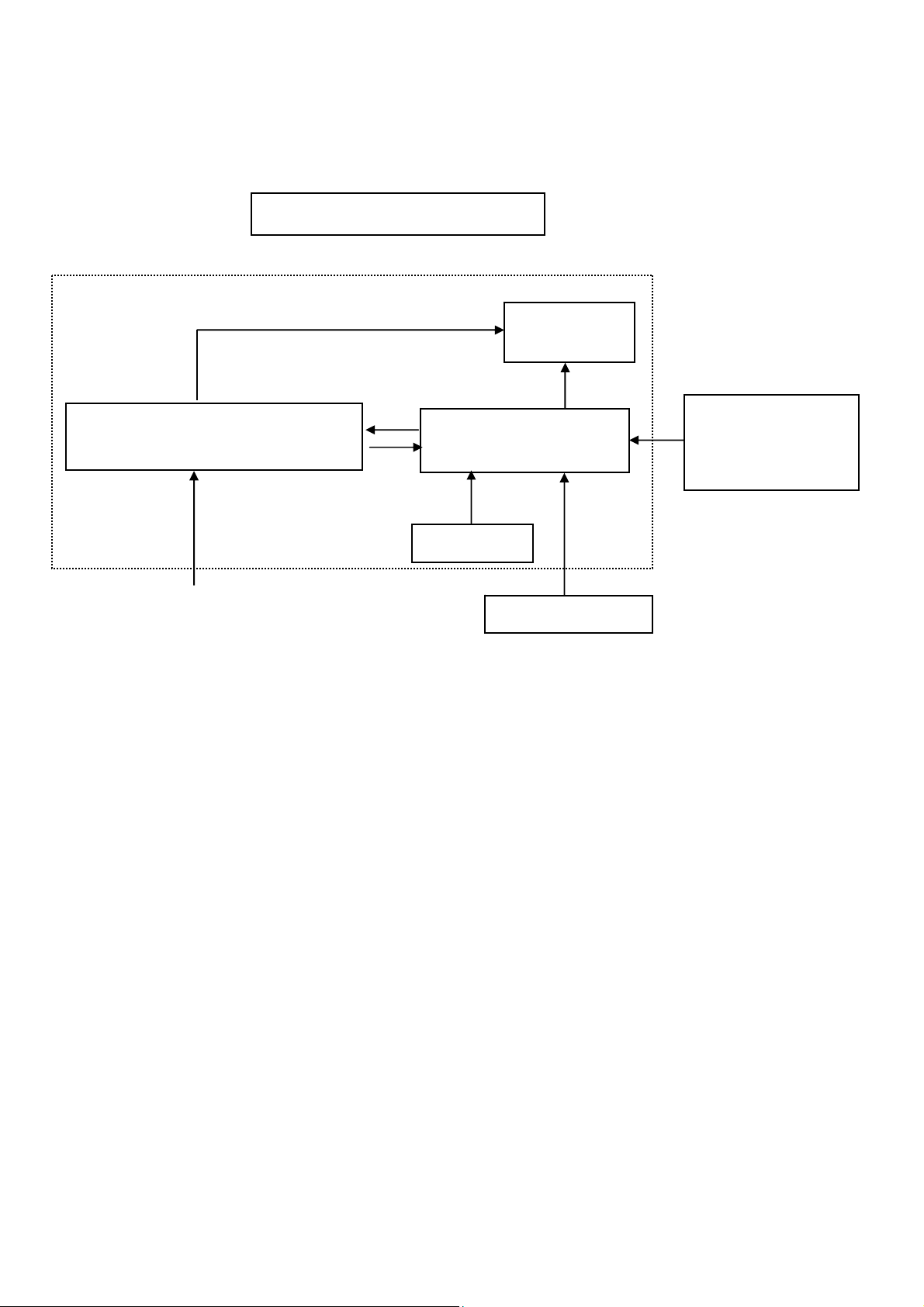
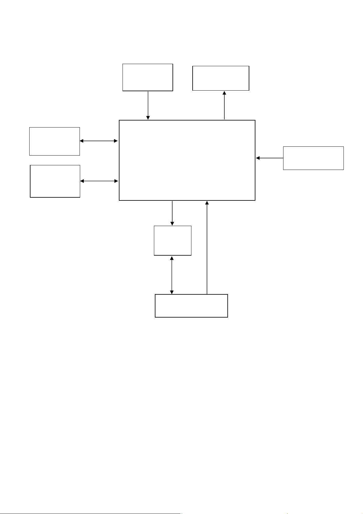
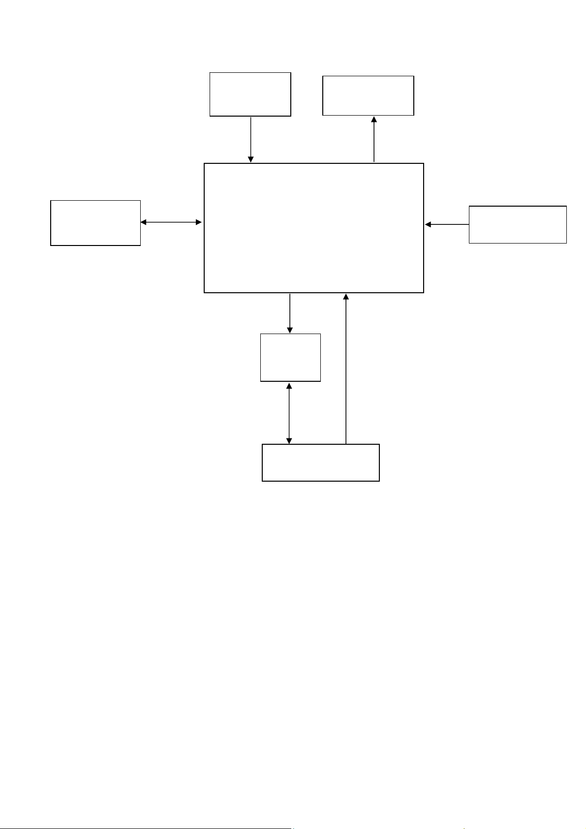
2. LCD Monitor Description
The LCD monitor will contain a main board, a power board and a key board which house the flat panel control logic,
brightness control logic and DDC.
The power board will provide AC to DC Inverter voltage to drive the backlight of panel and the main board chips
each voltage.
(Include: adapter, inverterd and audio)
Power board
Monitor Block Diagram
CCFL Drive.
Key Board
Flat Panel and
CCFL backlight
Main Board
RS232 Connector
For white balance
adjustment in factory
mode
AC-IN
100V-240V
HOST Computer
Video signal, DDC
5
Page 6
3. Operating Instructions
3.1 General Instructions
Press the power button to turn the monitor on or off. The other control buttons are located at front panel of the
monitor. By changing these settings, the picture can be adjusted to your personal preferences.
• The power cord should be connected.
• Connect the video cable from the monitor to the video card.
• Press the power button to turn on the monitor position. The power indicator will light up.
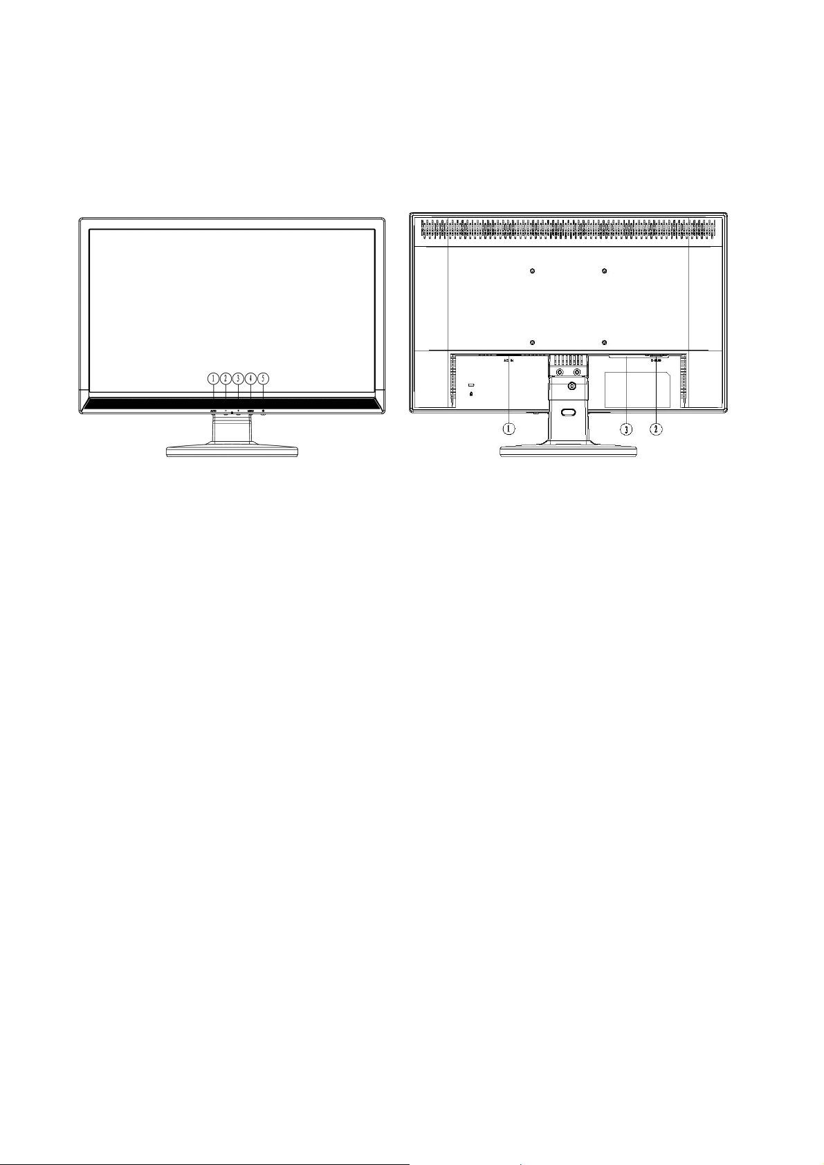
3.2 Control Buttons and Connections
1. Auto 1. Power Cord
2. -/Volume 2. Signal Cable
3. + /Volume 3. Audio Cable
4. MENU
5. Power Key
Power Button:
Press this button to switch on/off of monitor’s power.
MENU / ENTER:
Activates OSD menu when OSD is off or activate/de-activate adjustment function when OSD is on
-/Volume:
Activates the volume control when the OSD is OFF or navigate through adjustment icons when OSD is ON or adjust
a function when function is activated.
+/Volume:
Activates the volume control when the OSD is OFF or navigate through adjustment icons when OSD is ON or adjust
a function when function is activated.
Auto Adjust button / Exit:
1. When OSD menu is in active status, this button will act as EXIT-KEY (EXIT OSD menu).
2. When OSD menu is in off status, press this button over 2 seconds to activate the Auto Adjustment function.
The Auto Adjustment function is used to set the HPos, VPos, Clock and Focus.
Power Indicator:
Green — Power On mode
Orange — off mode
OSD Lock Function:
To lock the OSD, press and hold the MENU button while the monitor is off and then press power button to turn the
monitor on. To un-lock the OSD - press and hold the MENU button while the monitor is off and then press power
button to turn the monitor on.
6
Page 7
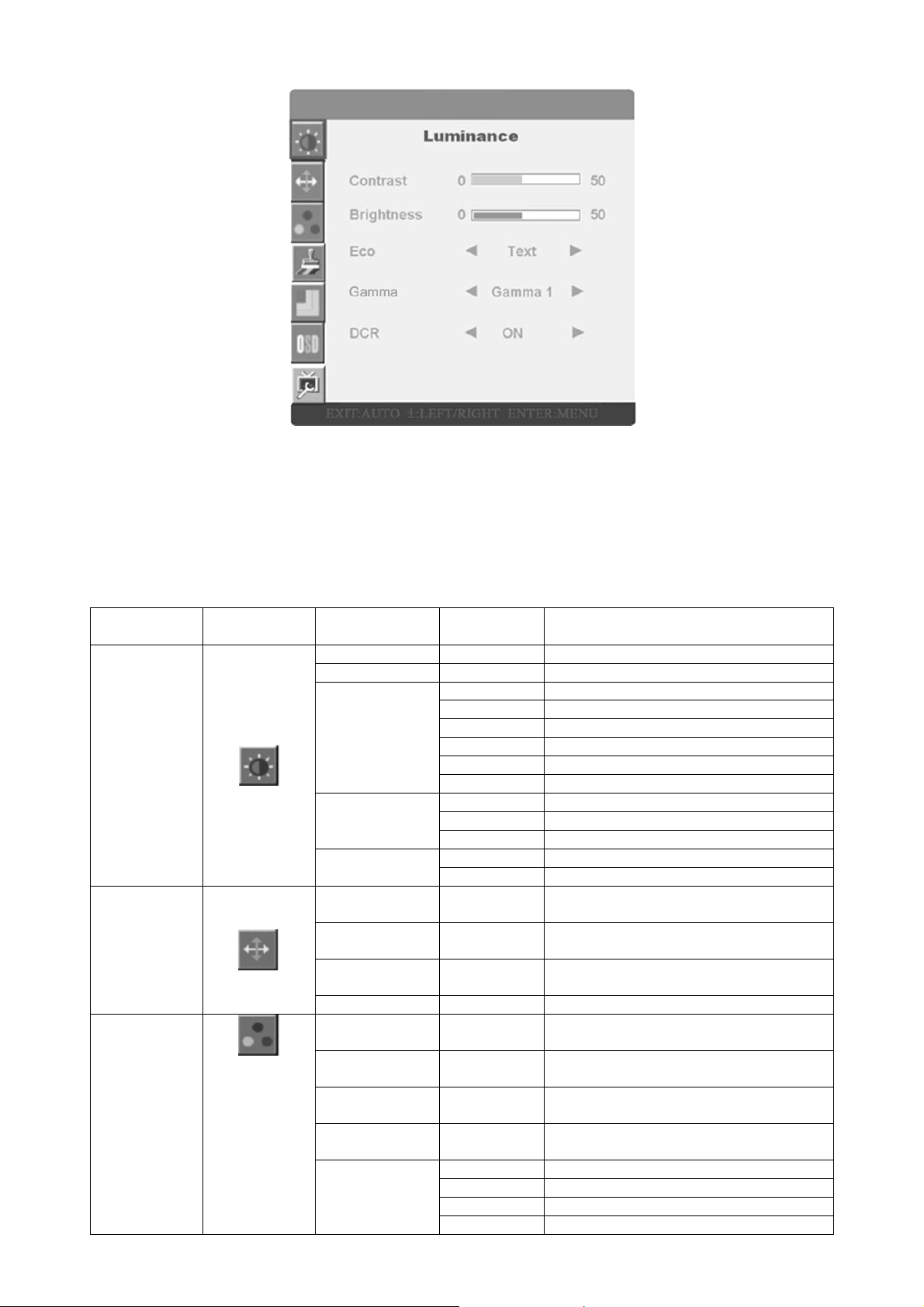
3.3 OSD Menu
• Press the MENU-button to activate the OSD window.
• Press – or + to navigate through the functions. Once the desired function is highlighted, press the
MENU-buttons to activate it. If the function selected has a sub-menu, press – or + again to navigate through
the sub-menu functions. Once the desired function is highlighted, press MENU-button to active it.
• Press – or + to change the settings of the selected function.
• To exit and save, selected the exit function. If you want to adjust any other function, repeat steps 2-3.
Function Control Illustration
Main Menu
Item
Luminance
Image Setup
Color Temp.
Main Menu
Icon
Sub Menu
Item
Brightness Backlight Adjustment
Contrast Contrast Digital-register
Eco
Gamma
DCR
Clock
Focus
H.Position
V.Position Adjust the vertical position of the picture
Warm
Normal
Cool
sRGB
User
Sub Menu Description
Standard Standard Mode
Text Text Mode
Internet Internet Mode
Game Game Mode
Movie Movie Mode
Sports Sports Mode
Gamma1 Adjust to Gamma1
Gamma2 Adjust to Gamma2
Gamma3 Adjust to Gamma3
Off Disable Dynamic Contrast Ratio
On Enable Dynamic Contrast Ratio
Adjust picture clock to reduce
Vertical-Line noise
Adjust Picture Phase to reduce
Horizontal-Line noise
Adjust the horizontal position of the
picture
Recall Warm Color Temperature from
EEPROM
Recall Normal Color Temperature form
EEPROM
Recall Cool Color Temperature from
EEPROM
Recall sRGB Color Temperature from
EEPROM
User-B Blue Gain from Digital-register
User-G Green Gain from Digital-register
User-R Red Gain from Digital-register
User-Y Yellow Gain from Digital-register
7
Page 8
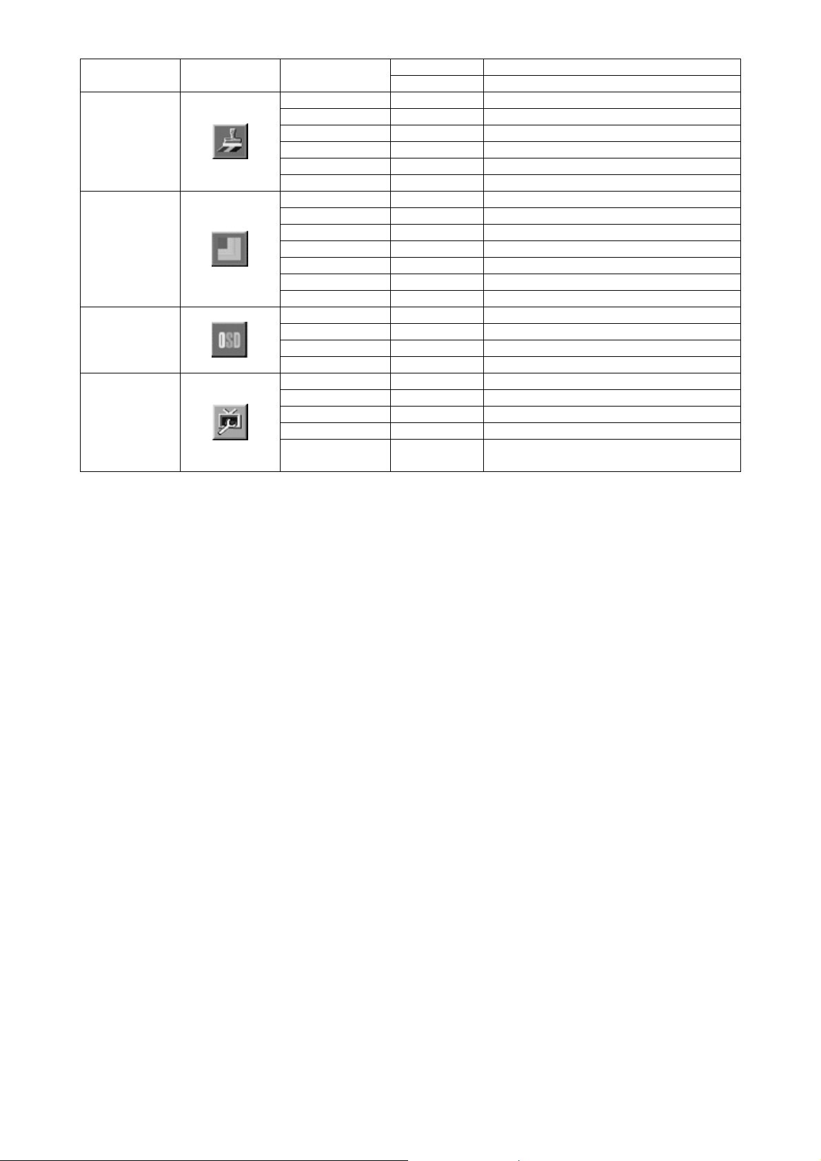
Color Boost
Picture
OSD Setup
Extra
User-C Cyan Gain from Digital-register
User-M Magenta Gain from Digital-register
Full Enhance On or off Disable or enable Full Enhance Mode
Nature Skin On or off Disable or enable Nature Skin Mode
Green Field On or off Disable or enable Green Field Mode
Sky-blue On or off Disable or enable Sky-blue Mode
AutoDetect On or off Disable or enable AutoDetect Mode
Demo On or off Disable or enable Demo
Frame Size Adjust Frame Size
Brightness Adjust Frame Brightness
Contrast Adjust Frame Contrast
Hue Adjust Frame Hue
Saturation Adjust Frame Saturation
Position Adjust Frame Position
Bright Frame On or off Disable or enable Bright Frame
H.Position Adjust the vertical position of OSD
V.Position Adjust the horizontal position of OSD
Timeout Adjust the OSD Timeout
Language Select the OSD language
Auto Config Auto adjust the picture to default
DDC/CI Turn on/off DDC/CI Support
Aspect Control Full/4:3
Reset Yes or no Reset the menu to default
Information
Show the information of the main image
and sub-image source
8
Page 9
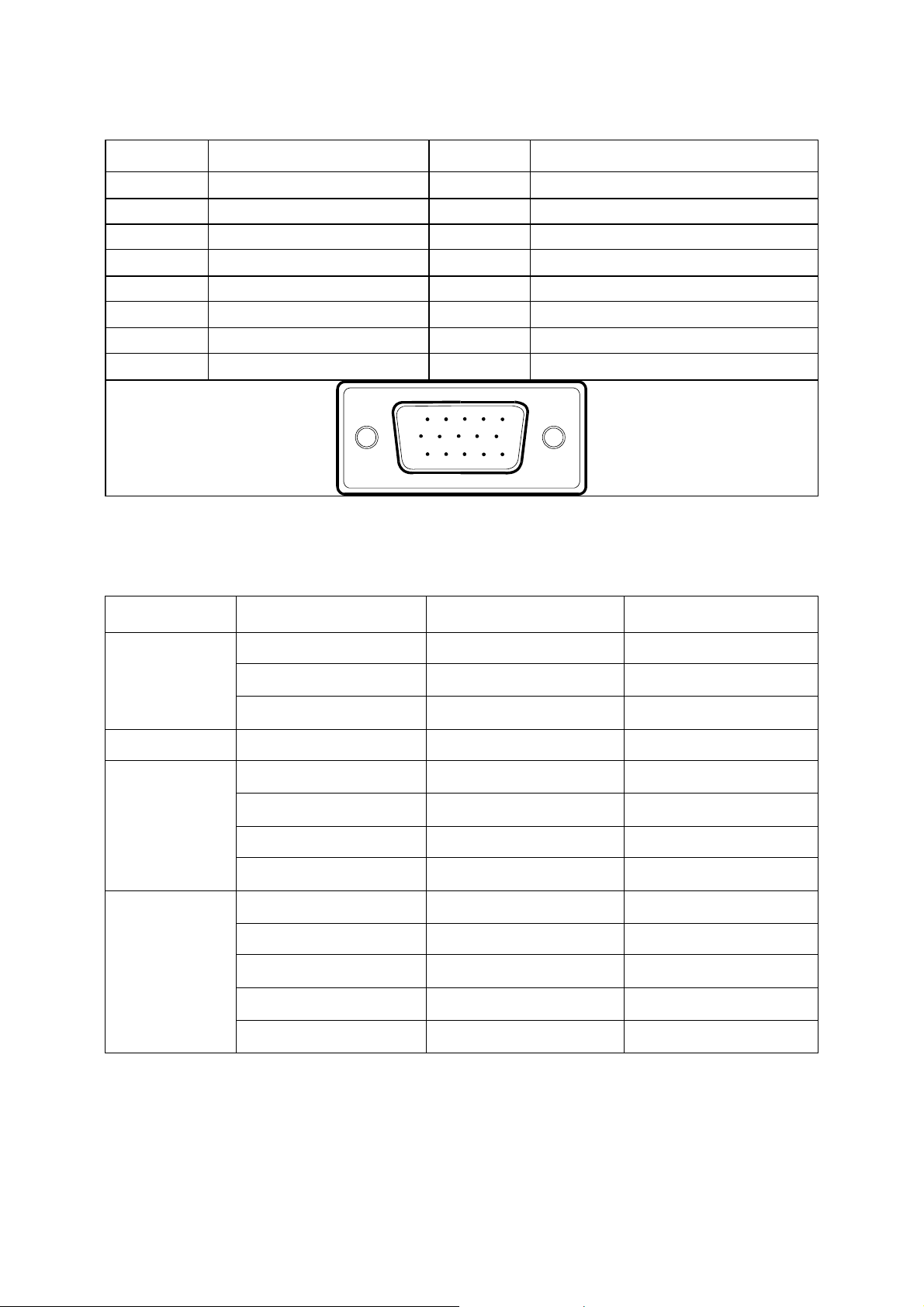
4. Input/Output Specification
4.1 Input Signal Connector
Analog connectors
Pin No. Description Pin No. Description
1 Red 9 +5V
2 Green 10
3 Blue 11
4 Ground 12 DDC-Serial data
5 Ground 13 H-sync
6 R-Ground 14 V-sync
7 G-Ground 15 DDC-Serial clock
8 B-Ground
Detect Cable
Ground
15
6
11 15
10
4.2 Factory Preset Display Modes
Standard Resolution
640×480 @60Hz 31.469 59.940
VGA
Dos-mode 720×400 @70Hz 31.469 70.087
SVGA
XGA
640×480 @72Hz 37.861 72.809
640×480 @75Hz 37.500 75.000
800×600 @56Hz 35.156 56.250
800×600 @60Hz 37.879 60.317
800×600 @72Hz 48.077 72.188
800×600 @75Hz 46.875 75.000
1024×768 @60Hz 48.363 60.004
1024×768 @70Hz 56.476 70.069
1024×768 @75Hz 60.023 75.029
Horizontal
Frequency(KHz)
Vertical
Frequency(Hz)
1360x768@60HZ 47.712 60.015
1366x768@60HZ 47.765 59.85
9
Page 10
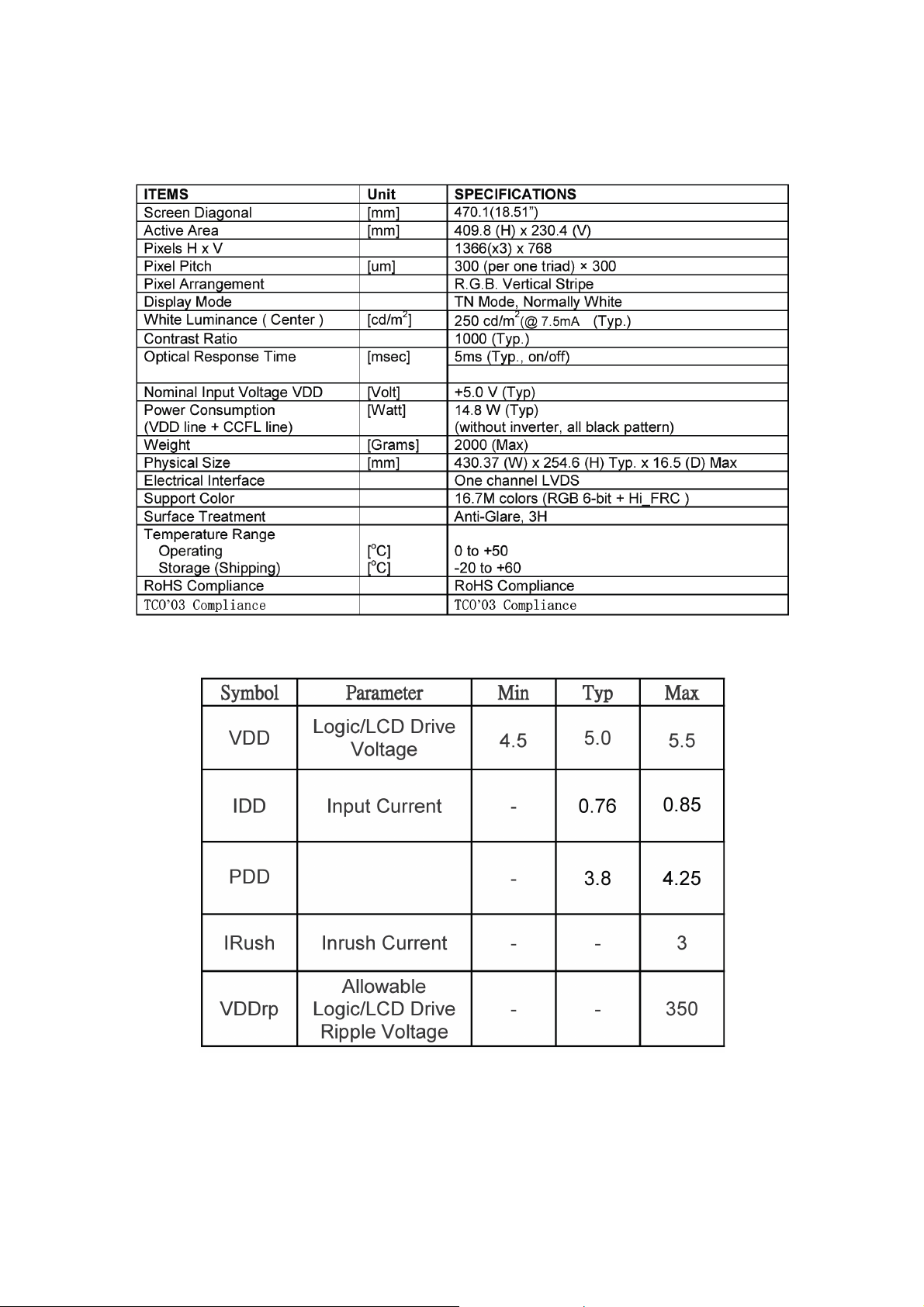
4.3 Panel Specification
4.3.1 General Features
This specification applies to the 18.5 inch-wide Color a-Si TFT-LCD Module M185XW01.The display supports the
WXGA - 1366(H) x 768(V) screen format and 16.7M colors (RGB 6-bits + Hi-FRC data). All input signals are
1-channel LVDS interface and this module doesn’t contain an inverter board for backlight.
4.3.2 Display Characteristics
4.3.3 Electrical Characteristics
(1) TFT-LCD
10
Page 11
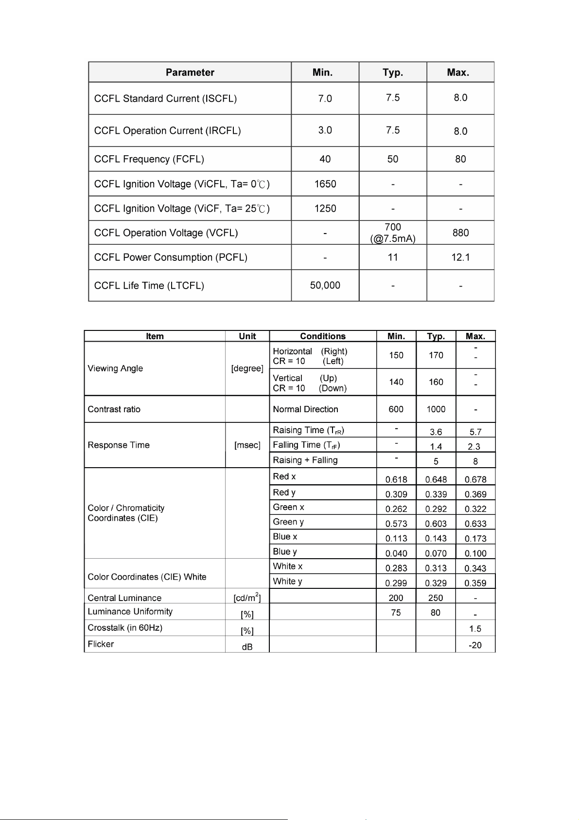
(2) Backlight
4.3.4 Optical Characteristics
11
Page 12
(
(
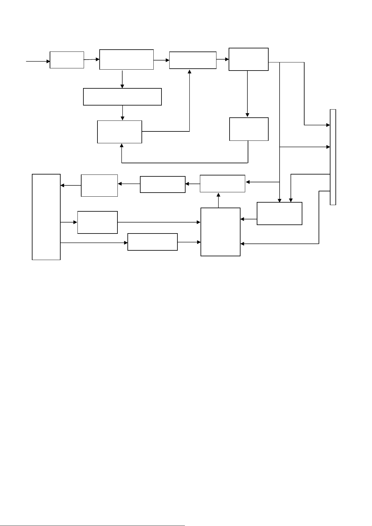
5. Block Diagram
5.1 Main Board
Crystal
24.576MHZ
(X401)
Panel Interface
(CN403)
FLASH ROM
SST25LF020A
U402)
EEPROM
M24C04
U406)
Scalar IC HX6803-A000LAG
(Include ADC, OSD, MCU)
(U401)
EEPROM
M24C02
(U101)
D-Sub Connector
(CN101)
DSUB_H
DSUB_V
DSUB_R+
DSUB_G+
DSUB_B+
DSUB_SOG
DDC1_SCL
DDC1_SDA
Key Control Interface
(CN408)
12
Page 13
(
715G3635M02000004L
FLASH ROM
MX25L2026DM1I
U402)
Crystal
24.576MHZ
(X401)
Scalar IC HX6810-A05MLAG
(Include ADC, OSD, MCU)
(U401)
EEPROM
M24C02
(U101)
Panel Interface
(CN405)
DSUB_H
DSUB_V
DSUB_R+
DSUB_G+
DSUB_B+
DSUB_SOG
DDC1_SCL
DDC1_SDA
Key Control Interface
(CN408)
D-Sub Connector
(CN101)
13
Page 14
5.2 Power Board
AC input
EMI filter
Bridge Rectifier
and Filter
Start Circuit: R904, R932
PWM
Control IC
Output
Circuit
Transformer
Transformer
MOSFET
Rectifier
diodes
Feedback
Circuit
CN902
5V
12V
ON/OFF
Lamp
Feedback
Circuit
Over Voltage
PWM
Control IC
(IC801)
ON/OFF
Control
DIM
14
Page 15
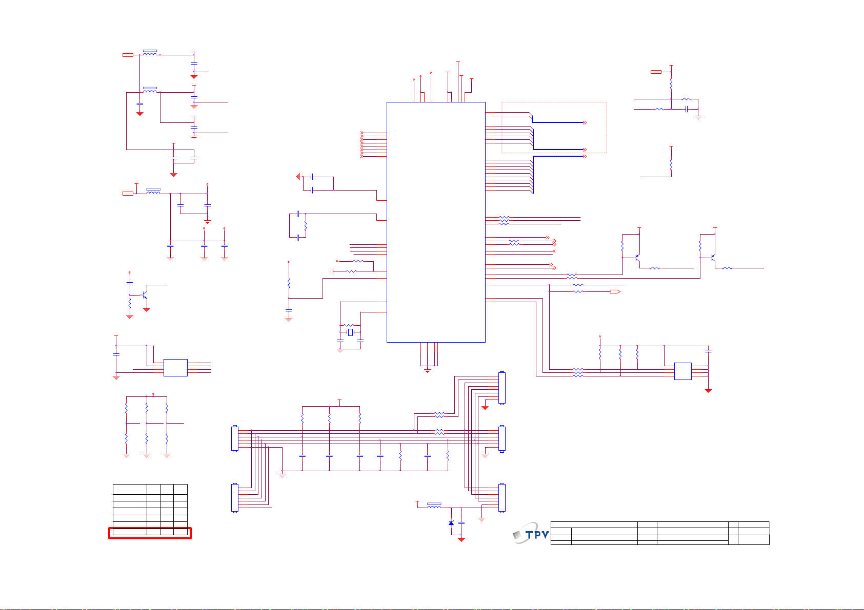
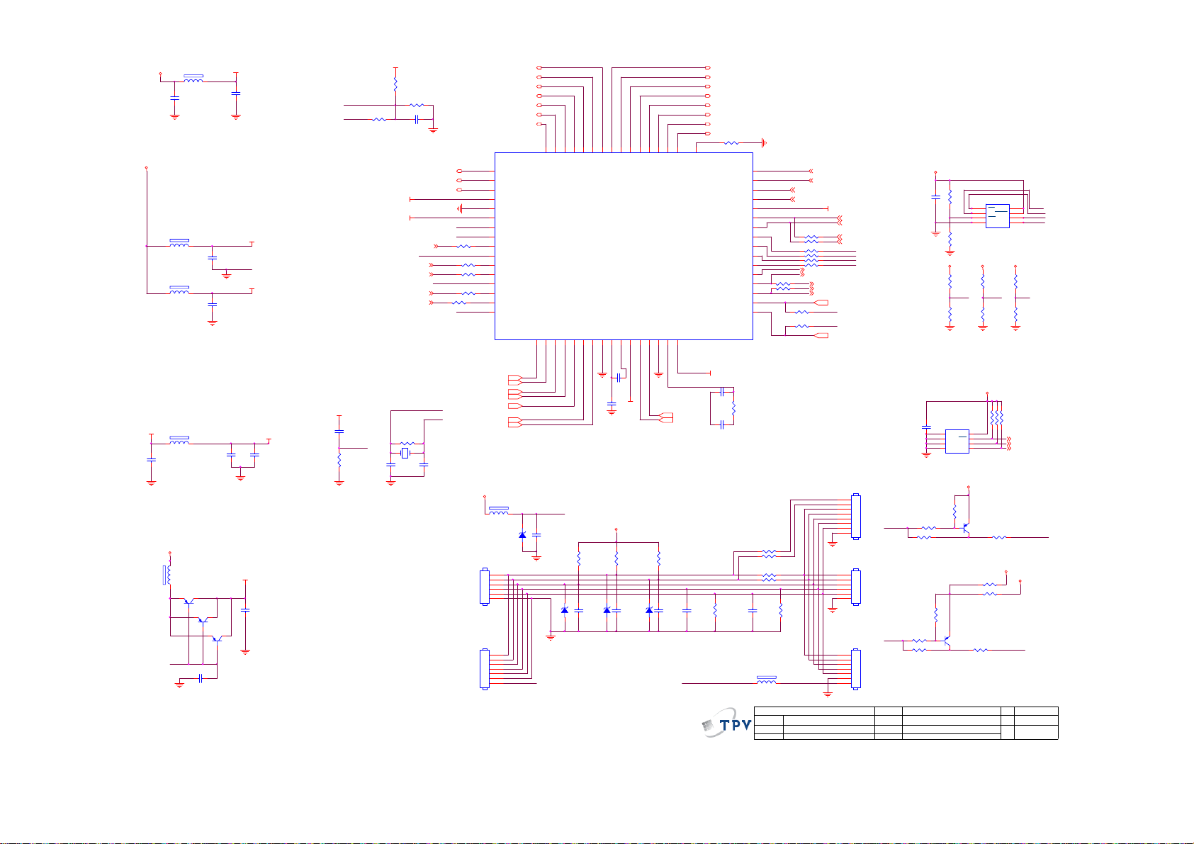
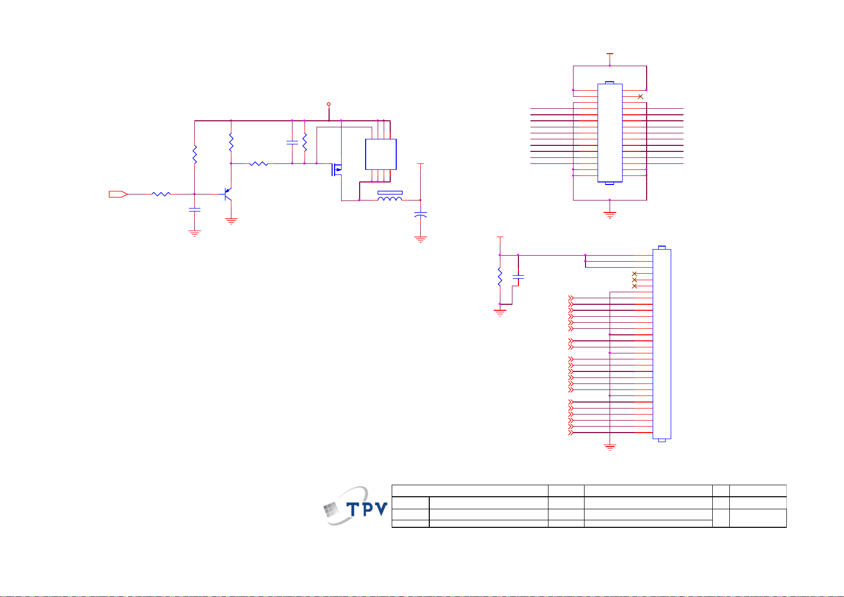
6. Schematic
6.1 Main Board
715G2681 1 4
DDC1_SCL3
DDC1_SDA3
DDC1_SCL
DDC1_SDA
R110
100R 1/16W 5%
R113
100R 1/16W 5%
H_Sync
R101 80 OHM
V_Sy nc
ZD103
UDZ SNP5.6B
C102
22pF
1 2
R105
2K2 1/16W 5%
CN101
DSUB_SCL VGA_PLUG
DSUB_SDA
15
14
13
12
11
10
5
9
4
8
3
7
2
6
1
DB15
17 16
R106
2K2 1/16W 5%
DSUB_5V
B_GND
VGA_B+
G_GND
VGA_G+
R_GND
VGA_R+ VGA_G+
R102 1K 1/16W 5%
R103 1K 1/16W 5%
C103
22pF
DSUB_5V
ZD104
UDZSNP5.6B
1 2
DSUB_5V 5
DSUB_H 3
DSUB_V 3
VGA_B+
B_GND
G_GND
R122
CHIP BEAD
R123
CHIP BEAD
R107
75R 1/ 16W 5%
R112
75R 1/ 16W 5%
C121
10pF
C120
10pF
R104
100R 1/16W 5%
R109
390 OHM 1/16W
R111
100R 1/16W 5%
C101
0.047uF
C106
0.047uF
C107
0.047uF
DSUB_B+ 3
DSUB_SOG 3
DSUB_G+ 3
GND POW ER DGND
DSUB_SDA
DSUB_SCL
VGA_G+
VGA_R+ VGA_B+
U103
1
I/O1
2
GND
I/O23I/O3
AZC099-04S
U102
1
I/O1
2
GND
I/O23I/O3
AZC099-04S
I/O4
VDD
I/O4
VDD
H_Sync
6
5
V_Sy nc
4
6
5
4
5V_ESD
ESD_5V
C115
47NF16V
C114
47NF16V
C118
0.1uF/16V
CMVCC15
CMVCC1
U101
1
A0
VCC
2
A1
WP
3
A2
SCL
VSS4SDA
M24C02-WMN6TP
5V_ESD
8
7
6
5
FB104
300 OHM
4K7 1/16W 5%
EDID _WP
DDC1_SCL
DDC1_SDA
VGA_R+
R_GND
2
R119
R124
CHIP BEAD
DSUB_5V
1
3
R120
10K 1/16W 5%
DSUB_5V 5
D105
BAV70
R121
10K 1/16W 5%
T P V ( Top Victory Electronics Co . , Ltd. )
絬 隔 瓜 絪 腹
Key Component
G2681-1-4-X-2-090226
Date
R116
75R 1/ 16W 5%
R115
100R 1/16W 5%
C122
10pF
DET_CABLE3
OEM MODEL
TPV MODEL
PCB NAME
Sheet
VCC3.3
C110
0.047uF
VCC3. 3 3,5
R118
1K 1/16W 5%
VGA_PLUG
4K7 1/16W 5%
715G2681 1 402.Input
of
25Thursday, February 26, 2009
R125
DSUB_R+ 3
EDID _WP
Q410
LMBT3904LT1G
15
Size
Rev
称爹
B
D
Page 16
VCC3.32,5
VCC1.85
CMVCC
VCC3.3
C408
0.22uF16V
R453
1K 1/16W 5%
R454
NC
POWER_ON_LATCH
POWER_ON_LATCH Setting
SPI-Flash
Spansion(2M)
SST-010A
PMC,MXIC(1M)
PMC,MXIC(2M)
SST-020A
1 2
1 2
VCC1.8
C456
1uF/16V
R482
10K 1/16W 5%
SPI_WP#
R452NCR451
R455
1K 1/16W 5%
FB405
BEAD
FB406
BEAD
C442
10uF/10V
FB409
1 2
220OHM
Q412
LMBT3904LT1G
VCC3.3
CSNSDO SCK
SDO
0
1
0
1
0
1
VCC3IO
C438
0.1uF/1 6V
C406
0.1uF/1 6V
C441
10uF/10V
RST
U402
8
SDO
VDD
7
CE#
HOLD#
3
WP#
SCK
VSS4SDI
SST25LF020A-33-4C-SAE
NC
R456
1K 1/16W 5%
SCK
CSN
0
0
0
0
1
0SST-010
0
1
0
1
0
0
VDDA_AD
VSSA_AD
VDDP_AD
VDDDP_AD
2
1
6
5
C404
0.1uF/1 6V
C433
0.1uF/1 6V
C403
0.1uF/1 6V
C439
0.1uF/1 6V
VCCK
SDI
CSN
SCK
SDO
C407
0.1uF/1 6V
C437
0.1uF/1 6V
VSSP_AD
VSSP_AD
VCCLVPVCCP
C436
0.1uF/1 6V
CN408
CONN
CN409
NC/CONN
6
5
4
3
2
1
7
6
5
4
3
2
1
TOUCH_POWER
GND
VDDP_AD
VCC3.3
GND
10K 1/16W 5%
C405 0.01uF /25V
R402
1K6 OHM 1/16W 5%
C409
0.1uF/1 6V
R450
5K1 OHM 1/16W 5%
C455
10uF/10V
R421
3.9K OHM 1/16W
C413
0.1uF/1 6V
C401
0.1uF/16V
VREF
C402
4.7uF/16V
R469 0R05 1/16W
GND
GND
VCC3.3
R427
C414
0.1uF/1 6V
Near to Connect
DSUB_B+2
DSUB_G+2
DSUB_SOG2
DSUB_R+2
DSUB_H2
DSUB_V2
DDC1_SDA2
DDC1_SCL2
R468 NCVCC3.3
RST
R401
XTAL_OUT
1M 1/16W 5%
X40 1
24.576MHz
C411
33pF
X1 GROUNG
SHIELDING
SDO
CSN
SCK
SDI
C412
33pF
R428
3.9K OHM 1/16W
KEY1
KEY2
POWER_KEY#
LED_GRN/BLUE
LED_ORAN GE
C415
0.1uF/1 6V
VCCP
6
B
7
G
8
SOG
9
R
11
HSYNC
12
VSYNC
17
DDCA_SDA/RS232_TX/GPIO17
18
DDCA_SCL/RS232_RX/GPIO18
4
VREF(1.25V)
14
FILT
22
SDO
23
CSN
24
SCK
25
SDI
62
TSTMD
63
RST_N
64
XTAL _O U T
1
XTAL _I N
R487
C416
10K 1/16W 5%
0.1uF/1 6V
VDDDP_AD
VCCLVP
VCC3IO
VCCK
30
54
41
2
32
52
VCCP(1.8V)
VCCK(1.8V)
VCCK(1.8V)
VCC3IO(3.3V)
VCCLVP(1.8V)
HX6803-A000LAG
LVDS
VSSP_AD
VSSA_AD
GNDIO
GNDIO
5
15
31
53
VSSA_AD
VSSP_AD
GNDIO
GNDIO
GND
R463 NC
R464 NC
R485 NC/1K
R486 NC/1K 1/16W 5%
R488
C417
10K 1/16W 5%
0.1uF/1 6V
FB404
VCC3.3
NC
ZD401
NC/UDZSNP5.6B
1 2
VDDA_AD
VDDP_AD
16
10
LVA3P
LVA3N
VCC3IO(3.3V)
VDDP_AD(3.3V)13VDDA_AD(3.3V)
LVA2P
VDDDP_AD(3. 3V)
LVA2N
LVA1P
LVA1N
LVA0P
LVA0N
LVB3P
LVB3N
LVBCKP
LVBCKN
LVB2P
LVB2N
LVB1P
LVB1N
LVB0P
LVB0N
PWMB/GPIO10
PWMC/GPIO11
PWMD/GPIO12
GPIO06
GPIO05
GPIO04/PWMC
GPIO03/PWMB
GPIO02/RS232_RX
GPIO01/RS232_TX
GPIO00/PWMD
USRD_MSC L/GPIO16
USRD_MSDA/ GPIO15
TOUCH_POWER
C445
NC
33
34
35
36
37
38
39
40
42
43
44
45
46
47
48
49
50
51
55
SAR0
56
SAR1
57
SAR2
58
59
60
3
61
29
28
27
26
19
21
20
U401
PA0
PA1
PA4
PA5
PA6
PA7
PA8
PA9
PB0
PB1
PB2
PB3
PB4
PB5
PB6
PB7
PB8
PB9
R411 100R 1/16W 5%
R412 100R 1/16W 5%
R420 100R 1/16W 5%
R419 NC /61G0402101
R418 N C/61G0402101
USRD_MSCL
USRD_MSDA
CN406
1
2
3
4
5
6
7
8
NC/CONN
CN402
1
2
3
4
5
6
NC/CONN
CN407
1
2
3
4
5
6
7
NC/CONN
SPI_WP#
UDP_WP
PA[0..1]
PA[4..9]
PB[0..9]
AC_DET
adj_BACKLIGHT 5
Mute 5
Volume# 5
DET_CABLE 2
on_Panel 4
on_BACKLIGHT 5
絬 隔 瓜 絪 腹
Key Component
PA[0..1] 4
PA[4..9] 4
PB[0..9] 4
KEY2
KEY1
10K 1/16W 5%
R415 4K7 1/16W 5%
R416 4K7 1/16W 5%
R480 NC
R490 N C/61G0402101
VCC3.3
R460
10K 1/16W 5%
R471 100R 1/16W 5%
R472 100R 1/16W 5%
100R 1/16W 5%
R473
T P V ( Top Victory Electronics Co . , Ltd. )
G2681-1-4-X-2-090226
Date
CMVCC5
R465
6K8 1/16W 5%
AC_DET
R466
POWER_KEY #
0R05 1/16W
R457
10K 1/16W 5%
SPI_WP#
VCC3.3 VCC3.3
R407
POWER_KEY #
PANEL_ID# 7
Q402
LMBT3906LT1G
R414
120R 1/16W 5%
USER DATA
R462
10K 1/16W 5%
R461
10K 1/16W 5%
OEM MOD EL
TPV MODEL
PCB NAME
Sheet
CMVCC
R467 10K 1/16W 5%
0.1uF/16V
VCC3.3
10K 1/16W 5%
LED_GRN/BLUE
U406
8
VCC
7
WC
6
SCL
5
M24C04-WMN6TP
715G2681-1-403.Scaler
of
35Thursday, February 26, 2009
C450
R404
NC
E1
E2
VSS4SDA
C444
0.22UF 10V
1
2
3
Q401
LMBT3906LT1G
R410
120R 1/16W 5%
Size
Rev
称爹
LED_ORANGE
Custom
D
16
Page 17
f
A
A
A
D
3
PANEL_VCC
on_Panel 3
1
G
O3401L
4K7 1/16W 5%
2
S
R435
on_Panel
PA[0..1]3
PA[4..9]3
R433
10K 1/16W 5%
Q404
LMBT3906LT1G
C446
NC/65G0402104 15
PA[0..1]
PA[4..9]
C419
0.1uF/16V
R436
13K OHM 1/16W 5%
C447
1uF 10V
PA0
PA1
PA4
PA5
PA6
PA7
PA8
PA9
R481
47K 1/16W 5%
Q405
PB[0..9]3
O3401
PB[0..9]
FB402
120OHM
VCC3.3D 5
PA1
CMVCCD 5
PANEL_VCC
C421
+
100UF25V
330 OHM 1/4W
PB0
PB1
PB2
PB3
PB4
PB5
PB6
PB7 PB2
PB8
PB9
PB3
PA5 PA4
PA7
PA9
PB1
PB3
PB7
PB9
PANEL_VCC
R434
CN403
CONN
2
4
6
PA0
8
PB2
10
12
PA6
14
PA8
16
PB0
18
PB2
20
PB4PB5
22
PB6
24
PB8
26
28
30
1
3
5
7
9
11
13
15
17
19
21
23
25
27
29
LVDS OUTPUT
C420
0.1uF/16V
PA0
PA1
PB2
PB3
PA4
PA5
PA6
PA7
PA8
PA9
PB0
PB1
PB3
PB4
PB5
PB6
PB7
PB8
PB9
10
11
12
13
14
15
16
17
18
19
20
21
22
23
24
25
26
27
28
29
30
1
2
3
4
5
6
7
8
9
CN405
NC/CONN
T P V ( Top Victory Electronics Co . , Ltd. )
? ? ? ? ? D
Key Component
Date
G2681-1-4-X-2-090226
OEM MODEL Size
TPV MODEL
PCB NAME
Sheet o
715G2681-1-404.Output
4 5Thursday, February 26, 2009
Rev
??
4
17
Page 18
ESD_5V
CN404
CONN
ESD_5V 2
CMVCC1 2
CMVCC 3
CMVCC1
CMVCCD 4
R449
NC
Mute 3
PANEL_ID#
FB407 300 OHM
CMVCC
9
8
7
6
5
4
3
2
1
CMVCC
CMVCC
BKLT_VBRI
BKLT_EN
Volume
Mut e
D402
SR24
R491 NC
D403
BAT54C
VCC3. 3 VCC3.3
R437
C425
NC
10K 1/16W 5%
R478 NC
Q406
LMBT3904LT1G
BKLT_EN
R440
4K7 1/16W 5%
R439
10K 1/16W 5%
on_BACKLI GHT 3
DSUB_5V
DSUB_5V2
CMVCC1
1
2
D401
NC/BAV70//93G 64 42 P
3
R438
3.3 OHM 2W
C431
0.1uF/ 16V
VI3VO
C424
+
100uF M 16V
U405
2
4
VO
GND
1
C432
0.1uF/ 16V
VCC1.8
C423
+
100uF M 16V
VCC1.8 3
BKLT_VBRI
R476
47R 1/16W 5%
VCC3.3
R441
10K 1/16W 5%
Q411
LMBT3904LT1G
4K7 1/16W 5%
R477
R475
10K 1/16W 5%
adj_BACKLI GHT 3
VCC3. 3 VCC3.3
R446
Volume
NC/10K 1/ 16W 5%
Q408
NC/57G 417 12 T
R448
NC
R447
NC
Volume# 3
CMVCC1
T P V ( Top Victory Electronics Co . , Ltd. )
絬 隔 瓜 絪 腹
Key Component
Date
MVCC
C426
+
100uF M 16V
G2681-1-4-X-1-090226
C428
0.1uF/16V
3
VIN
AP1117E33LA
U404
VSS
1
U403
1
ADJ(GND )
2
VOUT
3
VIN
NC/AP1117D 33LA
VOUT
4
4
2
OEM MO DEL
TPV MOD EL
PCB NAME
Sheet
FB408 NC,71G 56Z 601
C422
0.1uF/16V
715G2681-1-405.POWER
55Thursday , February 26, 2009
of
VCC3. 3
C427
+
100uF M 16V
VCC3. 3D
VCC3.3 2,3
VCC3.3D 4
Size
Rev
称爹
B
D
18
Page 19
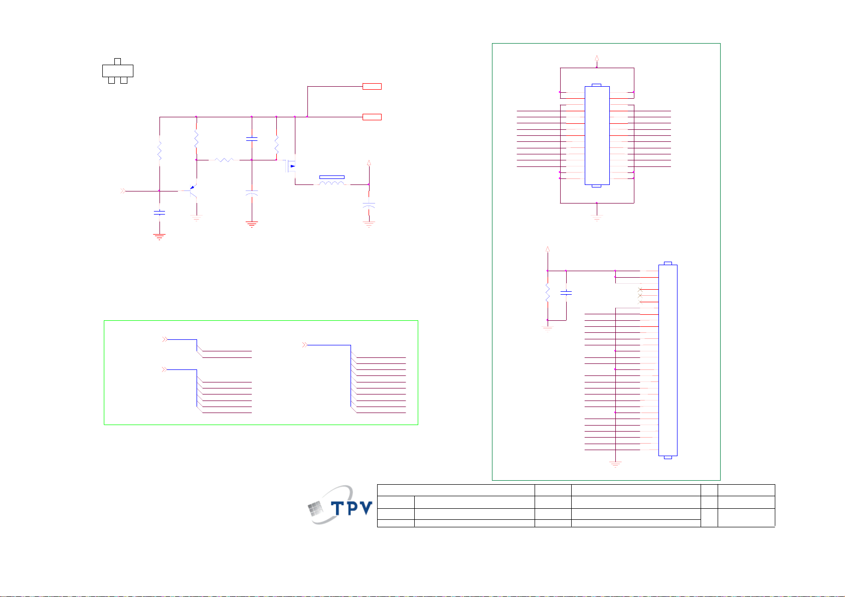
715G3635M02000004L
DB15
0R05 1/16W
SDA_VGA
SCL_VGA
15
14
13
12
11
R111
17 16
R105 0R05 1/10W 5%
R107
VGA_VS
VGA_HS
RXD3
CN101
10
5
9
4
8
3
7
2
6
1
2K2 1/16W 5%
VGA_PLUG
VGA_5V
B_GND
VGA_B
G_GND
VGA_G
R_GND
VGA_R
R109 0R05 1/16W
R110 100R 1/16W 5%
R113 100R 1/16W 5%
C102
R108
22pF
2K2 1/16W 5%
R106 1K1/16W
R104 1K1/16W
C103
22pF
VGA_5V
TXD 3
ZD104
RLZ5.6B
VGA_SDA
VGA_SCL
VGA_H
VGA_V
VGA_DDCA_SDA 3
VGA_DDCA_SCL 3
HSYNC 3
VSYN C 3
VGA_R
R_GND
VGA_B
B_GND
VGA_G
G_GND
FB101
1 2
BEAD
FB102
1 2
BEAD
FB103
1 2
BEAD
R122
R112
R116
75R 1/16W 5%
75R 1/16W 5%
75R 1/16W 5%
R114 22 OHM 1/16W
C111
NC
R115 56 OHM 1/16W
R117 22 OHM 1/16W
C108
NC
R118 56 OHM 1/16W
R119 22 OHM 1/16W
C104
R121 390 OHM 1/16W
NC
R120 56 OHM 1/16W
C101 0.047uF
C105 0.047uF
C107 0.047uF
C109 0.047uF
C110 0.047uF
C106 1000pF
C113 0.047uF
R3
GND_R 3
B3
GND_B 3
G3
SOG 3
GND_G 3
U103
SDA_VGA
SCL_VGA
VGA_G
VGA_R VGA_B
AZC199 -04S
1
I/O1
2
GND
I/O23I/O3
U102
AZC199 -04S
1
I/O1
2
GND
I/O23I/O3
I/O4
VDD
I/O4
VDD
6
5
4
VGA_PLUG
6
5
4
VGA_HS
VGA_VS
VGA_5V_S
候綼
U103
VGA_5V_S
候綼
U101
C115
NC
C114
NC
S_5V
VGA_5V
VGA_5V
1
2
D101
BAV70
3
C116
U101
1
A0
VCC
2
A1
WP
3
A2
SCL
VSS4SDA
M24C02-WMN6TP
VGA_5V_S
0.22uF
8
EDID _WP
7
VGA_SCL
6
VGA_SDA
5
FOR VGA DDC
R123
R124
R125
4K7 1/16W 5%
4K7 1/16W 5%
4K7 1/16W 5%
DET_CABLE_N3
VCC3D3
R127
1K1/16W
VGA_PLUG
T P V ( Top Victory Electronics Co . , Ltd. )
絬 隔 瓜 絪 腹
Key Component
Date
R126
3.3K 1/16W
G3635-M01-000-0040-9-10713
02.Inp ut
EDID _WP
Q101
LMBT3904LT1G
OEM MO DEL
TPV MODEL
PCB NAME
Sheet
G3635-M01-000-0040
26Tuesday, July 13, 2010
of
19
Size
Rev
称爹
B
1
<
称爹
>
Page 20
VCC3D3
VCC3D3
VCC1D8
10uF 10V
C441
VCC3D3
C426
10uF 10V
FB405
300 OHM
FB406
300 OHM
FB407
300OHM
FB409
NC
VCTRL
FB408
300 OHM
Q415
KN2907AS_NC
Q416
KN2907AS_NC
Q417
KN2907AS_NC
C449
0.1uF/ 16V_NC
C442
0.1uF/ 16V
C443
0.1uF/ 16V
VCC3IO
VSSP_AD
C425
0.1uF/ 16V
GNDIO
VDDP_AD
VDDDP_AD
C444
0.1uF/ 16V
VCC1D8
S_5V
R465
10K1/16W
AC_DET
POWER_KEY #
S_5V
C456
VCCK
C453
0.1uF/ 16V
C448
0.1uF/16V_NC
1uF/16V
RST_N
R482
10K 1/16W 5%
R429
0R05 1/16 W
C452
33pF
VCC3IO
XTAL_OUT
X40 1
GND
VCCK
1M 1/16W 5%
24.576MHz
R467 20K 1/16W
C450
0.1uF/ 16V
MUTE4
VCTRL
KEY1
KEY2
DET_CABLE_N2
VOL_PWM4
XTAL_OUT
R484
LVA1N5
LVA0P5
LVA0N5
XTAL _I N
C451
33pF
KEY1
KEY2
AC_DET
GNDIO
XTAL _O U T
XTAL _I N
R413
100R 1/16W 5%
R495100OHM1/16W
R496100OHM1/16W
R497 0R05
R489 100R 1/16W 5%
RST_N
VCC3D3
U401
49
FRSB1N/ LVA1N/ER6
50
FRSB2P/LVA0P/ ER5
51
FRSB2N/ LVA0N/ER4
52
VCC3IO (3.3V)
53
GNDIO (0V)/ GNDK (0V)
54
VCCK (1.8V)/ VCCP (1.8V)
55
XTAL _ O U T
56
XTAL _ I N
57
GPIO06
58
VCTRL_1.8
59
SAR0
60
SAR1
61
SAR3
62
PWMC/GPIO11
63
PWMD/GPIO12
64
RST_N
GND_B2
GND_G2
SOG2
GND_R2
FB404
NC
NC/U DZSNP5.6B
CN408
6
5
4
3
2
1
CONN
CN409
7
6
5
4
3
2
1
NC/CONN
LVA3P5
LVA3N5
LVACKP5
LVACKN5
LVA2P5
LVA2N5
LVA1P5
B2
G2
R2
ZD401
1 2
TOUC H_P OWER
40
42
45
41
43
46
48
47
44
FRSB0P/LVA2P/ EG1
FRSB1P/LVA1P/ ER7
FRSB0N/ LVA2N/EG0
FRSG1P/LVA3P/ EG5
FRSG0N/ LVB0N/EG6
FRSG1N/ LVA3N/EG4
FRSG2P/LVACKP/EG3
FRSG2N/ LVACKN/EG2
HX6810_A00
GIN_N
GIN_P4SOGIN
RIN_N6RIN_P7HVSS_AD(0V)8VRN9PVDDD_AD/HVDD_AD(3.3V)11HSYNC
BIN_P
BIN_N
3
5
2
1
TOUC H_PO WER
C445
NC
ZD404
NC/UDZSNP5.6B
R421
NC
1 2
C479
NC
R427
3.9K OHM 1/16W
C413
0.1uF/ 16V
ZD402
NC/U DZSNP5.6 B
VRN
VCC3D3
1 2
C457
1N 50V
10
VRP
C414
0.1uF/ 16V
NC/U DZSNP5.6B
39
36
35
37
38
FRSR2P/ LVB2P
FRSR2N /LVB2N
FRSCLKP/ LVB1P
FRSG0P/LVB0P/ EG7
FRSCLKN /LVB1N/EB0
VSYNC
VRP
PVSSD_AD(0V)14FILT15PVDDA_AD(3.3V)
13
12
VDDDP_AD
R428
3.9K OHM 1/ 16W
C415
0.1uF/ 16V
ZD403
1 2
34
33
TSTMD
FRSR0P/ LVB3P
FRSR0N /LVB3N
GPIO02/RS232_RX/GPIO30
GPIO01/R S232_TX/GPIO31
DDCA _SCL/RS2 32_RX/GPIO30
DDCA_SDA/RS232_TX/GPIO31
16
VSYNC 2
HSYNC 2
KEY1
KEY2
POWER_KEY #
LED_GRN/BLUE
LED_ORANGE/TOUCH VCC
C416
0.1uF/16V
LED_ORANGE/TOUCH VCC
LVB0N 5
LVB0P 5
LVB1N 5
LVB1P 5
LVB2N 5
LVB2P 5
LVB3N 5
LVB3P 5
R401 4K7 1/16W 5%
PWMB/GPIO10
GPIO05
GPIO04/PW MC
GPIO03/PWMB
VCCK (1.8V)
USRD_MSCL/GPIO16
USRD_MSDA/GPIO15
GPIO00/PW MD
VDDP_AD
C455 0.01uF/25V
VDDP_AD
C454
0.1uF/16V
R487
10K 1/16W 5%
GND
32
31
30
29
28
RS_RXD
27
RS_TXD
26
25
SDI
24
SCK
23
CSN
22
SDO
21
20
19
18
17
R402
1K6 OHM 1/16W 5%
R463 NC
R464 NC
R485 NC/1K 1
R486 NC/1K 1/16W 5%
C417
0.1uF/ 16V
FB410
NC
T P V ( Top Victory Elect ronics Co . , Ltd. )
絬 隔 瓜 絪 腹
Key Component
Date
SPI_WP#
PANEL_ON/OF F 5
BL_PW 4
R403 NC
R404 NC
R491 0R05 1/16W
R476 0R05 1/16W
R441 0R05 1/16W
R446 0R05 1/16W
USRD_MSCL
USRD_MSDA
R459 NC
R490 NC
UDA_WP
R493 NC
R494 NC
R488
10K 1/16W 5%
TOUC H_PO WER
G3635-M01-000-0040-9-1 0713
02.Input
BL_ADJ 4
SPI_WP#
PANEL_ID# 4
POWER_KEY #
UDA_WP
VCCK
LED_G
LED_O
RXD 2
TXD 2
SDI
SCK
CSN
SDO
VGA_DDCA_SCL 2
KEY1
KEY2
VGA_DDCA_SDA 2
CN406
1
2
3
4
5
6
7
8
NC/CONN
CN402
2
3
4
5
6
NC/CONN
CN407
1
2
3
4
5
6
7
NC/CONN
LED_G
LED_O
OEM MODEL
TPV MODEL
PCB NAME
Sheet
VCC3D3
C458
0.22uF16V
C459
NC
R405
R448 10K 1/ 16W 5%
R408 NC
R406
2.2K1/16W
R492
10K 1/16W 5%
R498
NC
G3635-M01-000-0040
of
36Tuesday, July 13, 2010
R409
10K1/16W
SPI_WP#
R410
NC
R471NCR472
SDO
R474
10K1/16W
U406
1
NC
VCC
2
E1
WC
3
E2
SCL
VSS4SDA
NC
S_5V
2.2K1/16W
Q402
LMBT3906LT1G
U402
1
CS
VCC
2
SO
HOLD
3
WP
SCK
GND4SI
MX25L2026DM1I-12G
NC
CSN SCK
R480
10K1/16W
VCC3D3
R411NC
R415NC
8
7
6
5
Q422
LMBT3906LT1G
R462 300R 1/ 10W 5%
VCC3D3
R433 NC
R436 0R
LED_ORANGE/TOUCH VCC
R499 330R 1/ 10W 5%
VCC3D3VCC3D3 VCC3D3
NC
10K1/16W
R416NC
UDA_WP
USRD_MSCL
USRD_MSDA
Size
Rev
称爹
8
7
6
5
R473
R481
LED_GRN/BLUE
S_5V
SDI
CSN
SCK
SDO
C
1
称爹
>
<
20
Page 21

S_5V
CN404
9
8
7
6
5
4
3
2
1
CONN
S_5V S_5V
BKLT_EN
C427
NC
5V_SYS
5V_SYS
BKLT_VBRI
BKLT_EN
Volume
Mut e
R437
10K 1/16W 5%
Q406
2N3904S-RTK/PS
R440
4K7 1/16W 5%
5V_SYS
VOL_PWM 3
Mut e 3
R439
10K 1/16W 5%
BL_PW 3
S_5V
NC
R400
PANEL_ID# 3
S_5V 2,3,5
BKLT_VBRI
S_5V
R475
10K 1/16W 5%
R477
100R 1/16W 5%
BL_ADJ 3
+
C428
100uF M 16V
S_5V
3
C431
0.1uF/ 16V
R438
3.3 OHM 2W
C435
0.1uF /16V
U404
VIN
AP1117E33LA
1
U403
1
ADJ(GND )
2
VOUT
3
VIN
NC
VI3VO
U407
1
ADJ(GND )
2
VOUT
3
VIN
NC
VSS
VOUT
4
U405
1
VCC3D3
2
4
VO
GND
C430
0.1uF/ 16V
2
4
C432
0.1uF/ 16V
+
C429
100uF M 16V
VCC1D8
+
VCC3D3 2, 3
C434
100uF M 16V
T P V ( Top Victory Electronics Co . , Ltd. )
絬 隔 瓜 絪 腹
Key Component
G3635-M01-000-0040-9-10713
02.Input
Date
OEM MODEL
TPV MO DE L
PCB NAME
Sheet
G3635-M01-000-0040
of
46Tuesday , July 13, 2010
Size
Rev
称爹
B
1
称爹
>
<
21
Page 22
PANEL_VC C
CN405
CONN
2
4
6
PA0
8
PB2
10
PA4
12
PA6
14
PA8PA9
16
PB0
18
PB2
20
22
PB6
24
PB8
26
28
30
CN403
1
2
3
4
5
6
7
8
9
10
11
12
13
14
15
16
17
18
19
20
21
22
23
24
25
26
27
28
29
30
1
11
13
15
17
19
21
23
25
27
29
PA0
PA1
PB2
PB3
PA4
PA5
PA6
PA7
PA8
PA9
PB0
PB1
PB2
PB3
PB4
PB5
PB6
PB7
PB8
PB9
3
5
7
9
5V_SYS
C302
0.22uF16V
R307
NC
Q405
NC
R305
R308
4K7 1/16W 5%
PANEL_ON/ OFF3
R304
100OHM1/16W
C478
NC
10K 1/16W 5%
R306 56K 1/ 16W
Q404
LMBT3906LT1G
4
3
G
5
120OHM
S1S2S
D8D7D6D
FB402
Q401
AO4411
PANEL_VCC
C305
+
100UF25V
PANEL_VCC
R435
330 OHM 1/ 4W
PA1
PB3
PA5
PA7
PB1
PB3
PB5 PB4
PB7
PB9
LVDS OUTPUT
C436
0.1uF/ 16V
LVB3P3
LVB3N3
LVACKP3
LVACKN3
LVB2P3
LVB2N3
LVB1P3
LVB1N3
LVB0P3
LVB0N3
LVA3P3
LVA3N3
LVACKP3
LVACKN3
LVA2P3
LVA2N3
LVA1P3
LVA1N3
LVA0P3
LVA0N3
NC/CONN
T P V ( Top Victory Electronics Co . , Ltd. )
絬 隔 瓜 絪 腹
Key Component
Date
G3635-M01-000-0040-9-10713
02.Input
OEM MO D EL
TPV MODEL
PCB NAME
Sheet
G3635-M01-000-0040
56Tuesday , J uly 13, 2010
of
Size
Rev
称爹
A4
1
<
称爹
>
22
Page 23

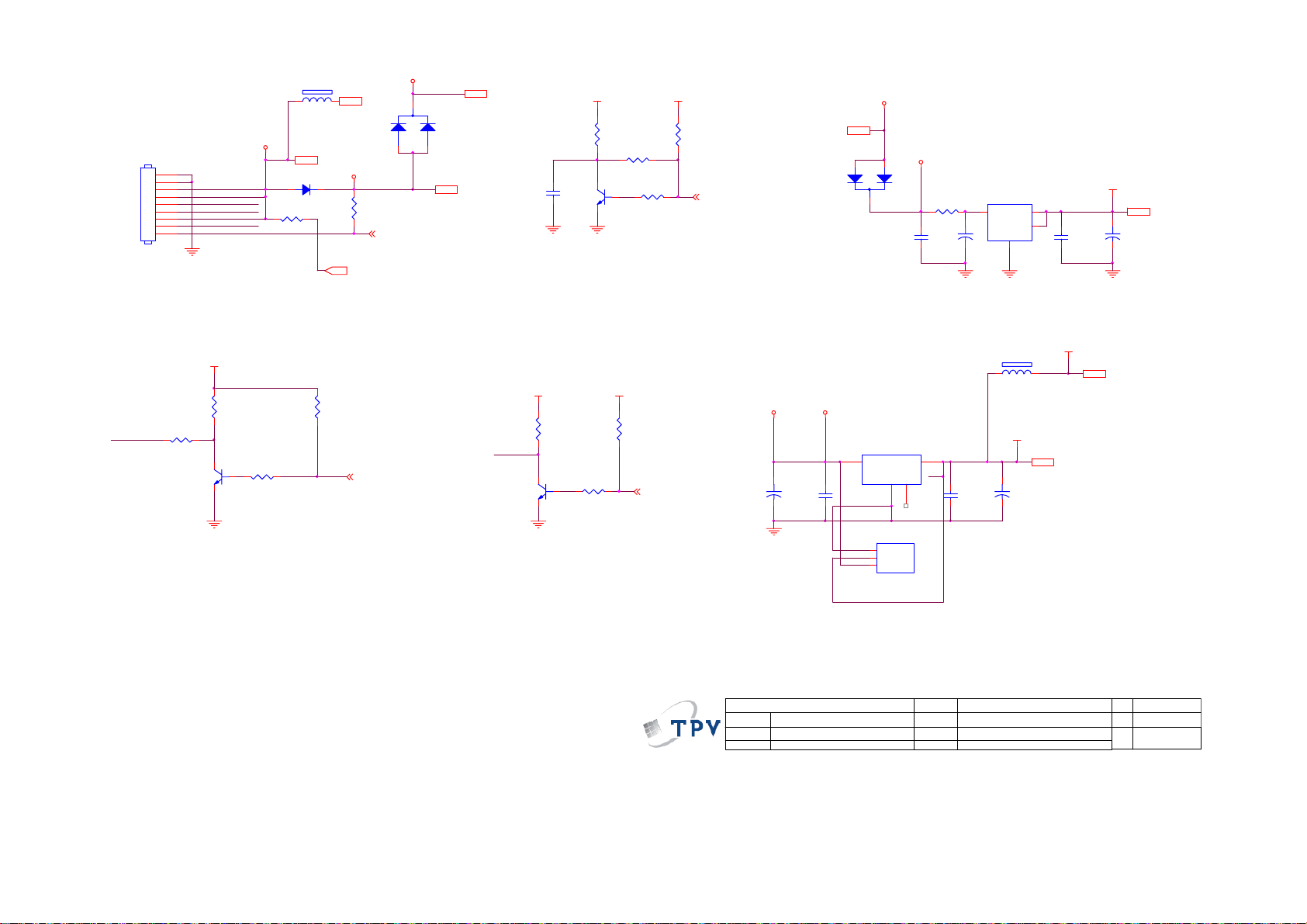
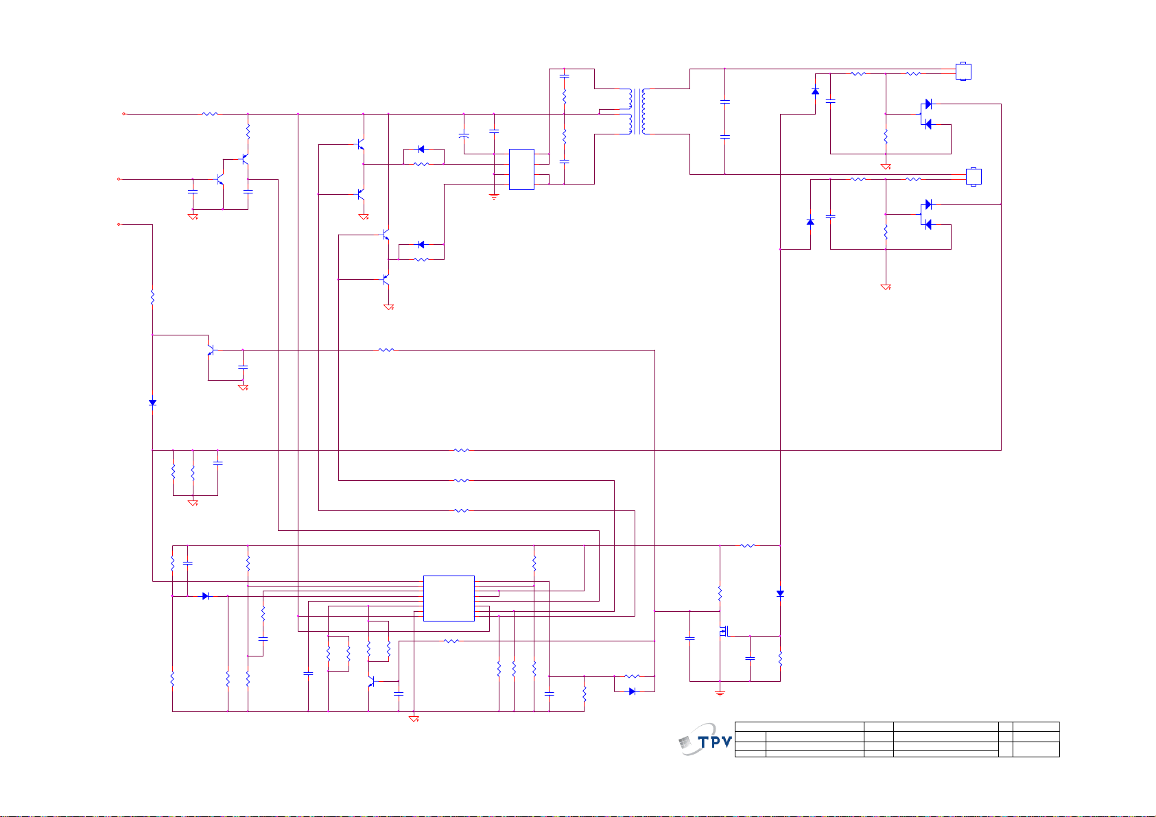
6.2 Power Board
715G2852 3 4
1
!
+
1000pF
R900
680K OHM 1/4W
!
t
2
BD901
KBP208G
C902
!
NR901
NTCR
!
!
0.22UF
680K OHM 1/4W
CN901
SOCKET
87G 501 32 DL
0.22UF
2
1
C908
R902
VAR901
Varistor
N.C
3
-
4
C904
!
3
4
C901
1000pF
L901
30mH
12
3
!
!
!
!
R901
680K OHM 1/4W
!
!
!
R915
100K OHM 1% 1/8W
0.01uF
!
F901
FUSE
+
C907
100uF450V
C938
NC
C911
0.1uF
IC901
1
RT
2
COMP
NC
3
CS
VCC
GND4OUT
LD7575A PS
C928
GND1
GND
1
2
HS2
HEAT SINK(D906_Q90G6263-6)
1
2
HS3
HEAT SINK (Q901_Q90G6263-6)
1
2
R904
8.2K OHM 1/4W
R932
8.2K OHM 1/4W
8
HV
7
6
5
R905
NC
R906
NC
+
R907
NC
D903
LL4148
R910
10R 1/4W
ZD905
RLZ18B
R912
220 OHM 1/4W
C909
470pF/25V
HS5
SHIELD(H 85G0002-1)
1
2
D901
FR103
C903
22uF/50V
1 2
C906
1500pF2KV
R938
10K 1/8W
R908
100KOHM +- 5% 2WS
D900
FR107
R909
5.1 OHM 1/4W
!
Q901
2SK2645-54MR
R914
0.47 OHM +-5% 2W S
4
5
6
2
1
!
C900
3300pF 250V
!
T901
POWER X'FMR
43
9
10
7
8
11
12
12
IC902
PC123X2YFZOF
IC903
AZ431AZ-AE1
R918
100 OHM 1/4W
R919
100 OHM 1/4W
R920
100 OHM 1/4W
R921
R922
R923100 OHM 1/4W
R961 100 OHM 1/4W
R962 100 OHM 1/4W
R935 100 OHM 1/4W
C924
0.1uF
C912
0.001uF
2
1
3
D906
FCH10U10
D907 31DQ06FC3
100 OHM 1/4W
100 OHM 1/4W
D905 31DQ06FC3
C929
0.001uF
R925
1K 1/8W
R926
1K 1/10W 1%
C925
NC
L904
1.0uH
+
+
C917
680uF/25V
C910
0.001uF
絬 隔 瓜 絪 腹
Key Component
C918
680uF/25V
L905
1.0uH
+
C921
470uF/16V
+
C939
820uF25V
3904
L903
R924
150R 1/8W
2.43K OHM 1% 1/10W
G2852-3-4-X-8-100610
2.POWER
1.0uH
1K 1/10W 1%
C940
+
1000UF25V
T P V ( Top Victory Electronics Co . , Ltd. )
Date
+
R948
56 OHM
Q904
ZD922
RLZ5.1B
D916
LL4148
C922
470PF50V
R942
R930
ZD923
RLZ5.6B
1 2
R946
150 OHM 2W
Q903
PMBS3904
C932
0.001uF
1 2
R947
470R
R952
1K 1/8W 5%
C915
MUTE
DIM
of
VOL
+5V
R940
33K 1/10W
470uF/16V
C931
0.1uF
ZD921
RLZ13B
1 2
R927
3.6K OHM 1% 1/10W
D915
LL4148
ON/OF F
OEM MO DEL
TPV MOD EL
PWPC85 21VYD2 A
PCB NAME
715G2852-A-4
Sheet
24Thursday, J une 10, 2010
+
ZD902
RLZ13B
1 2
R943
470R 1/8W
R939
1K 1/8W
0R05 1/4W
F902
NC
F904
F903
NC
F905
0 OHM 1/4W
Size
Rev
称爹
C930
0.1uF
10
1
2
3
4
5
6
7
8
9
+12V
+5V1
+5V
CN902
CONN
Custom
ODM MO DEL
23
Page 24
1
2
D801
BAV99
D802
BAV99
CONN
CN801
2
1
1
2
CONN
CN802
2
1
ON/OF F
C839
1500PF/50V
R855
+12V
DIM
F801
0 OHM 1/4W
Q805
PDTC144WK
C807
0.1uF/25V
R804
100R 1/8W
Q808
PDTA144WK
C825
0.1uF/25V
PMBS3904
Q804
PMBS3906
C802
Q801
23
1
PMBS3904
Q811
D810
NC
R839
22R 1/8W
D811
NC
470UF/25V
+
C824
0.1uF
Q802
AM9945N-T1-PF
1
S
2
G
3
S
4
G
15R 1/4W
R856
15R 1/4W
8
D
7
C838
D
1500PF/50V
6
D
5
D
POWER X'FMR
6
3
4
T801
R821
1K 1/8W
3
R801
1K5 1/10W 1 %
R822
1K 1/8W
3
R814
1K5 1/10W 1 %
7
C801
30pF/3KV
81
C803
30pF/3KV
D807
LL4148
D805
LL4148
C819
0.0022uF
C823
0.0022uF
R817
10K 1/10W 1%
R828
10K 1/10W 1%
D817
LL4148
6K8 1/10W
10K 1/10W 1%
R827
1K 1/10W 1%
R851
R830
NC
R820
Q806
PMBS3904
R802
8.2K 1/10W 1%
C822
1uF/25V
D812
LL4148
R863
10K 1/10W 1%
C842
0.01uF
C835
NC
R832
10K 1/10W 1%
R831
1K 1/8W
R823
0R05 1/10W 5%
C821
0.1uF/25V
51K OHM 1% 1/8W
R810
C820
220pF50V
PMBS3906
R865
NC
Q812
1
R853
68K 1/10W
R861
1M 1/10W 1%
Q807
PMBS3904
R850
23
22R 1/8W
R841
68K OHM 1% 1/10W
R829
22R 1/8W
R825
22R 1/8W
R837
47K 1/8W
R807
R824
1K 1/10W 1%
10K 1/10W 1%
R808
10K 1/10W 1%
C845
2.2uF/ 16V
R862
1M 1/10W 5%
R803
680K 1/10W
D814
LL4148
C846
NC
C834
0.01uF/ 25V
G2852-3-4-X-8-100610
3.IN VERTER
R835
NC
D806
LL4148
R818
1K 1/10W 1%
Q809
RK7002
T P V ( Top Victory Electronics Co . , Ltd. )
絬 隔 瓜 絪 腹
Key Component
Date
OEM MOD EL
TPV MOD EL
PCB NAME
Sheet
715G2852-A-4
of
34Thursday , June 10, 201 0
Custom
Size
Rev
A
ODM MO DEL
称爹
R864
NC
C817
NC
1
2
3
4
5
6
7
8
IC801
1IN+
1INFEEDBACK
DTC
OUTPUT CTRL
CT
RT
GND
C1
680K 1/10W
R854
TL494IDR
2IN+
2INREF
VCC
16
15
14
13
12
11
C2
10
E2
9
E1
R826
1K 1/8W
24
Page 25

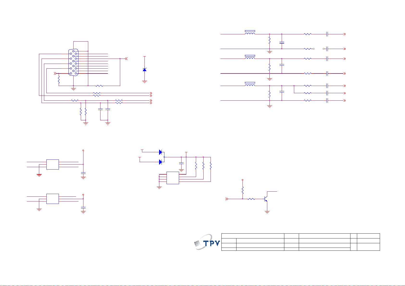
CN601
PHONEJACK
+5V1
C602 0.47uF/ 16V
C603 0.47uF/ 16V
R602
10K 1/10W 5%
VOL
R603
10K 1/10W 5%
MUTE
LIN
4
5
3
RIN
2
1
R604 10K 1/ 10W 5%
R605 10K 1/ 10W 5%
C609
1uF/25V
C601 0.47uF /16V
C606 0.47uF /16V
R601
10K 1/10W 5%
100uF/25V
8
SE/BTL
7
VOLUME
6
LIN -
5
GND
4
GND
3
RIN-
2
BYPASS
1
SHUTDOWN
C604
APA2069JITUL
IC601
+
LOUT-
VDD
LOUT+
GND
GND
ROUT+
VDD
ROUT-
CONN
9
10
11
12
13
14
15
16
LOUT-
LOUT+
ROUT+
ROUT-
4
3
2
1
CN602
R608
1R 1/ 8W
100pF
R606
C610
5.6K O HM 1/10W
R607
C611 100pF
5.6K O HM 1/10W
C612
0.1uF/ 16V
C613
0.1uF/ 16V
C608
1uF/25V
IC with Heat-sink(90G6295-3)
FB602
1 2
BEAD
T P V ( Top Victory Electronic s Co . , Lt d. )
絬 隔 瓜 絪 腹
Key Component
Date
G2852-3-4-X-8-100610
4.AUDI O
OE M MOD EL
TPV MODEL
PCB NAME
Sheet
715G2852-A-4
of
44Thursday , J une 10, 2010
Size
Rev
称爹
A
A
ODM MODEL
25
Page 26

6.3 Key Board
715G2835 2
CN001
LBADC 1
1
LBADC 2
2
DC_POWER ON
3
LED_GR N#
4
LED_RED#
5
6
CONN
SGND
LBADC1
LBADC2
OK
UP
DOWN
MENU
(0)
(2K)
(1K)
C001
NC/0.001uF
1.435V(2.0K)
1.042V
1.042V
1.435V
C002
NC/ 0.001uF
LED_RED#
C003
NC/0.001uF
1
LED_GRN#
3
LED001
LED
2
C004
NC/ 0.001uF
C005
NC/0.001uF
R002 2K 1/10W
R003 0R05 1/10W 5%
R004 2K 1/10W
R005 1K 1/10W 5%
C007NC /0.1uF
GND
ZD002NC/UDZS5.6B
SW005
3 4
SGND
OK
21
5
SW
SGND
UP
SW004
21
5
SW
ZD005NC/UDZS5.6B
C009NC /0.1uF
3 4
SGND
SGND
SW003
POWER
21
5
SW
ZD003NC/UDZS5.6B
C010NC /0.1uF
3 4
SGND
SGND
ZD004NC/UDZS5.6B
C008NC /0.1uF
SGND SGND
SW002
3 4
DOWN
21
5
SW
SW001
MENU
21
5
SW
ZD001NC/UDZS5.6B
C006NC /0.1uF
3 4
SGND
SGND
(Power)
(MENU)
(UP)
LED
(DOWN)
(OK)
CONNECTOR
T P V ( Top Victory Electronics Co . , Ltd. )
絬 隔 瓜 絪 腹
Key Component
G2835-A-X-X-1-070802
2.0.k ey
Date
OEM MO DE L Size
TPV MODEL
PCB NAME
AOC Q-W19
Q19W A
715G2835
Sheet
of
22Friday , August 10, 2007
Rev
称爹
26
B
称爹
>
<
Page 27

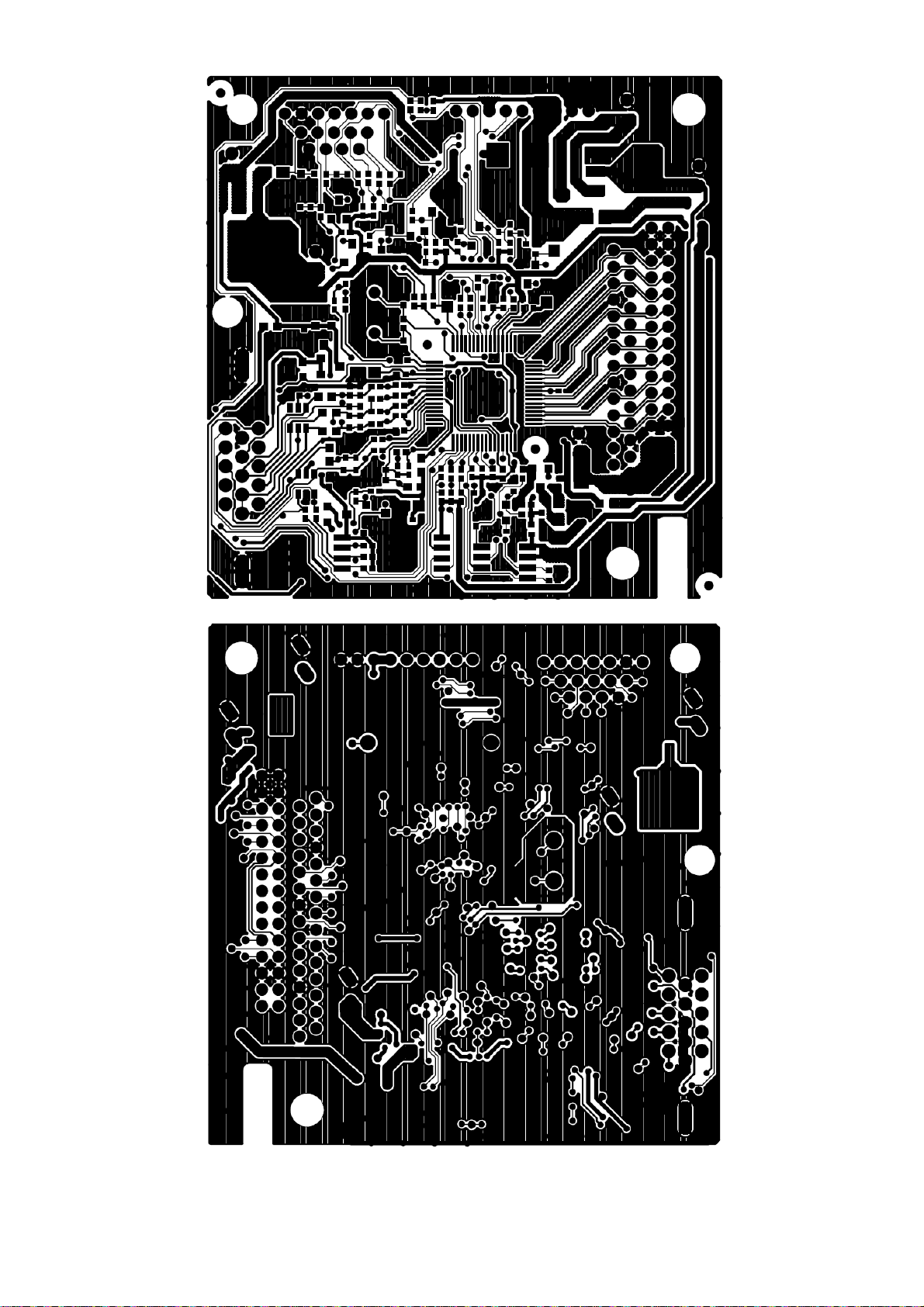
7. PCB Layout
7.1 Main Board
715G2681 1 4
27
Page 28
28
Page 29

715G3635M02000004L
29
Page 30

30
Page 31

7.2 Power Board
715G2852 3 4
31
Page 32

32
Page 33

7.3 Key Board
715G2835 2
33
Page 34

8. Maintainability
8.1 Equipments and Tools Requirement
1. Voltmeter.
2. Oscilloscope.
3. Pattern Generator.
4. DDC Tool with an IBM Compatible Computer.
5. Alignment Tool.
6. LCD Color Analyzer.
7. Service Manual.
8. User Manual.
34
Page 35

8.2 Trouble Shooting
8.2.1 Main Board
1. No Power
Check power cable is
Check Power “On/Off”
Replace the power board and check connections
Replace main board and check connections
Replace key board and check connections
No power
tightened?
OK
is “On”?
OK
Check the LED
indicate is OK?
OK
NG
NG
NG
Re-plug the power cable
NG
Turn on the Power “On/Off” switch
NG
Check the AC power
35
Page 36

2. No Video (Power LED Green)
No Video (Power LED Green)
Press the power
button is OK?
OK
Replace the power
board and connection
NG
Replace the main
board and connection
NG
Check the LVDS/FFC
cable or panel
NG
OK
OK
OK
Replace the main board
The end
The end
Replace the LVDS/FFC
cable or panel
NG
Replace the key board
36
Page 37

q
y
3. DIM
DIM (image overlap, focus or flicker)
Reset in factory mode
NG
Set to the optimal
frequency, select the
recommended fre
NG
Readjust the phase and pixel
clock in the user mode
NG
Pull out signal cable and
check “Self Test Feature
Check” is ok?
NG
Replace the main board
uenc
OK
The end
OK
The end
OK
The end
OK
Check the signal cable
and the PC
NG
OK
The end
NG
Replace the panel
OK
37
Page 38
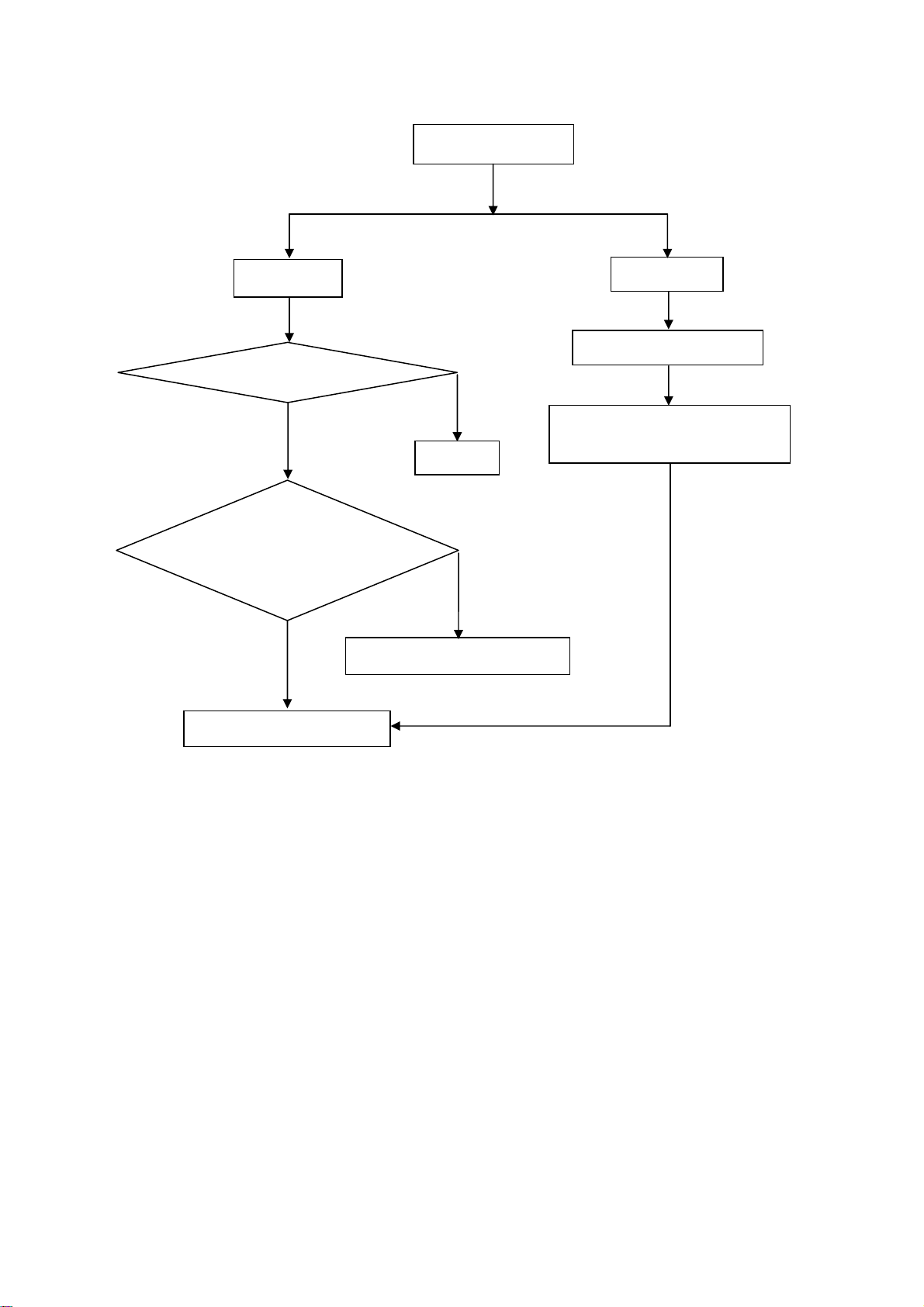
4. Color is not optimal
Color is not optimal
Miss color
Color shift
Replace the signal cable
NG
OK
The end
Reset the factory mode
NG
In the user mode, set the” color
settings” until customer satisfy
Pull out the signal cable
and check the screen
color display is normal?
NG
OK
NG
Replace the signal cable or PC
Replace the main board
38
Page 39

9. White- Balance, Luminance Adjustment
Approximately 30 minutes should be allowed for warm up before proceeding white balance adjustment.
How to setting MEM channel you can reference to chroma 7120 user guide or simple use “ SC” key and
“ NEXT” Key to modify xyY value and use “ID” key to modify the TEXT description Following is the procedure to
do white-balance adjust .
1. Setting the color temp.
A. MEM.CHANNEL 3 (Warm color):
2
Warm color temp. parameter is x = 313 ±30, y = 329 ±30, Y=180cd/ m
B. MEM.CHANNEL 4 (Normal color):
Normal color temp. parameter is x = 302 ±30, y = 318 ±30, Y=180cd/ m
C. MEM.CHANNEL 9(Cool color):
Cool color temp. parameter is x = 283 ±30, y = 297 ±30, Y=180cd/ m
D. MEM.CHANNEL 10 (sRGB color):
sRGB color temp. parameter is x = 313 ±30, y = 329 ±30, Y=180cd/ m
2. Enter into the factory mode:
AC off, when press the MENU button, AC on. Then press the MENU button again, you will enter into the factory
(typ)
2
(typ)
2
2
(typ)
mode.
3. Gain adjustment:
Move cursor to “-F-” and press MENU key
A. Adjust Warm (6500K) color-temperature
1. Switch the chroma-7120 to RGB-Mode (with press “MODE” button)
2. Switch the MEM.channel to Channel 3 (with up or down arrow on chroma 7120)
2
3. The LCD-indicator on chroma 7120 will show x = 313 ±30, y = 329 ±30, Y=180cd/ m
(typ)
4. Adjust the RED on factory window until chroma 7120 indicator reached the value R=100
5. Adjust the GREEN on factory window until chroma 7120 indicator reachedthe value G=100
6. Adjust the BLUE on factory window until chroma 7120 indicator reached the value B=100
7. Repeat above procedure (item4, 5, 6) until chroma 7120 RGB value meet the tolerance =100±2
B. Adjust Normal (7300K) color-temperature
1. Switch the chroma-7120 to RGB-Mode (with press “MODE” button)
2. Switch the MEM.channel to Channel 4(with up or down arrow on chroma 7120)
3. The LCD-indicator on chroma 7120 will show x = 301 ± 30, y = 317± 30, Y=180cd/ m
2
4. Adjust the RED on factory window until chroma 7120 indicator reached the value R=100
5. Adjust the GREEN on factory window until chroma 7120 indicator reachedthe value G=100
(typ)
6. Adjust the BLUE on factory window until chroma 7120 indicator reached the value B=100
7. Repeat above procedure (item 4, 5, 6) until chroma 7120 RGB value meet the tolerance =100±2
C. Adjust Cool (9300K) color-temperature
1. Switch the Chroma-7120 to RGB-Mode (with press “MODE” button)
2. Switch the MEM. Channel to Channel 9 (with up or down arrow on chroma 7120)
2
3. The LCD-indicator on chroma 7120 will show x = 283 ±30, y = 297 ±30, Y=180cd/ m
(typ)
4. Adjust the RED on factory window until chroma 7120 indicator reached the value R=100
5. Adjust the GREEN on factory window until chroma 7120 indicator reached the value G=100
6. Adjust the BLUE on factory window until chroma 7120 indicator reached the value B=100
39
Page 40

7. Repeat above procedure (item 4, 5, 6) until chroma 7120 RGB value meet the tolerance =100±2
D. Adjust sRGB color-temperature
1. Switch the chroma-7120 to RGB-Mode (with press “MODE” button)
2. Switch the MEM.channel to Channel 10 (with up or down arrow on chroma 7120)
2
3. The LCD-indicator on chroma 7120 will show x = 313 ±30, y = 329 ±30, Y=180cd/ m
4. Adjust the RED on factory window until chroma 7120 indicator reached the value R=100
5. Adjust the GREEN on factory window until chroma 7120 indicator reachedthe value G=100
6. Adjust the BLUE on factory window until chroma 7120 indicator reached the value B=100
7. Repeat above procedure (item 4, 5, 6) until chroma 7120 RGB value meet the tolerance =100±2
E. Turn the Power-button off to quit from factory mode.
40
Page 41

10. Monitor Exploded View
41
Page 42

11. BOM List
Note: The parts information listed below are for reference only, and are subject to change without notice. Please go
to http://cs.tpv.com.cn/hello1.asp
T89AHDNCWX1UAN
for the latest information.
Location
040G 581909 1A PROTECT LABEL
044GH600 1 HANDLE 2
050G 600 4 HANDLE 1
052G 1185 1 BIG TAPE(Y1200141)
052G 1207 A TASMA ALUMINIOWA
052G 1211 B CONDUCTIVE TAPE 85MM *40MM *0.09MM
052G 2191 A PAPER TAPE
078G 32210C Y NO-SUGGEST SPK 8 OHM 1.5W 43X18 250 100M
089G 725CAA DB D-SUB CABLE
089G417A15N IS POWER CORD
095G8014 6XH54 HARNESS 6P(PLUG)-6P(PLUG) 140
E09501 095G8018 3LH92 HARNESS 30P-30P(2004) 140MM
E09501 095G8018 3XH92 LVDS CABLE 30P-30P(2004) 140MM 2nd source
0G1G1130 8120 SCREW
0M1G1030 6120 SCREW M3X6
705GQ834166 19" LCD STAND-BASE ASS'Y
AM1G1740 10 47 CR3 SCREW
Q12G6600 6 FOOT
Q34G0266ABJ 1B0100 STAND TOP
Q34G0267ABJ 1B0120 STAND
Q34G0268ABJ 1B0133 BASE 8S1
M037 Q37G0067015 HINGE
M037 SQ37G0067015 HINGE ASS'Y
015F0067510 SUPPORT
015F0067020 ACTIVE PLATE
004F0610051 01 WASHER
004F061210T 01 METAL WASHERS12.0*4.72*1.0T
004F061210M 00 METAL WASHERS12.0*6.03*4.70H
004F0612052 00 METAL WASHER
028F0817070 SHAFT
0M1F3050106 SCREW
002F0605100 SCREW NUTS M6.0*P1.0
E750 750GLU185X1233N000 PANEL M185XW01 V20B XM AUO
E750 750GLU185X1243N000 PANEL M185XW01 V20C XM AUO 2nd source
756GQ9CB AW098 MAIN BOARD-CBPC9HDA9QA
U402 056G1133 81 SST25LF020A-33-4C-SAE
SMTC9-U402 100GAHA8001YT1 MCU ASS'Y-056G1133 81
A15G0842501 MAINFRAME
AM1G1740 12 47 CR3 SCREW
040G 45762412B CBPC LABEL
CN408 033G3802 6B Y CONN 6PIN 2.0
CN404 033G3802 9B Y CONNECTOR 9P 2.0
R438 061G152M339 64 CHIPR 3.3 OHM +-5% 2W
CN101 088G 35315F HD D-SUB CONN F ATTACHED SCREW 2nd source
CN101 088G 35315F XH D-SUB 15PIN VERTICAL CONN WITH SCREW
X401 093G 2258B J CRYSTAL 24.576MHZ 20PF 49US
CN403 311GW200C30ABL WAFER 2.0MM 2*15P
C421 067G 3151014KB EC LOW ESR 100UF M 25V 6.3*11MM
U102 056G 662 13 IC AZC099-04S SOT23-6L
Part No. Description Remark
42
Page 43

U103 056G 662 13 IC AZC099-04S SOT23-6L
U401 056G1126 48 IC HX6803-A000LAG LQFP-64
U406 056G1133 32 IC M24C04-WMN6TP SO8
U101 056G1133 34 M24C02-WMN6TP
U402 056G1133 81 SST25LF020A-33-4C-SAE
Q411 057G 417 12 T KEC 2N3904S-RTK/PS
Q406 057G 417 12 T KEC 2N3904S-RTK/PS
Q410 057G 417 12 T KEC 2N3904S-RTK/PS
Q412 057G 417 12 T KEC 2N3904S-RTK/PS
Q405 057G 763 1 AO3401 SOT23 BY AOS
R109 061G04023900FI TEST ONLY RST 0402 390R 1% 1/16W TA-I
R481 061G0402473 JI TEST ONLY RST 0402 47K 5% 1/16W TA-I
C456 065G0805105 12 1UF +-10% 16V X7R
C441 065G0805106 A7 CHIP 10UF 10V Y5V 0805
C442 065G0805106 A7 CHIP 10UF 10V Y5V 0805
FB407 071G 56G301 EA CHIP BEAD T1201209G301NP100
FB402 071G 56K121 M CHIP BEAD 120OHM 6A MGLB2012-120T-LF
FB405 071G 59K190 B 19 OHM BEAD
FB406 071G 59K190 B 19 OHM BEAD
R122 071G 59K190 B 19 OHM BEAD
R123 071G 59K190 B 19 OHM BEAD
R124 071G 59K190 B 19 OHM BEAD
R101 071G 59K800 CHIP BEAD 80 OHM FCM1608K-800
D403 093G 60230 NO-SUGGEST BAT54C SOT23
D402 093G2004 2 DIODE SR24
715G2681 1 4 MAIN PCB FR-4 D/S 65*64*1.6MM
FB104 071G 59G301 CHIP BEAD 300OHM
FB409 071G 59S221 M CHIP BEAD 0603 220OHM+-25% 2A
Q406 057G 417518 TRA LMBT3904LT1G 200MA/40V SOT-23 LRC
Q410 057G 417518 TRA LMBT3904LT1G 200MA/40V SOT-23 LRC
Q412 057G 417518 TRA LMBT3904LT1G 200MA/40V SOT-23 LRC
Q408 057G 417 12 T KEC 2N3904S-RTK/PS
U405 056G 133 33AAC LDO AZ1117H-1.8TRE1
U405 056G 56327A IC AP1117E18L-13
U404 056G 563514 IC AZ1117H-3.3TRG1 1A/3.3V SOT223
U404 056G 585 4A IC AP1117E33L-13
Q404 057G 417 6 PMBS3906/PHILIPS-SMT(06)
Q402 057G 417 6 PMBS3906/PHILIPS-SMT(06)
Q401 057G 417 6 PMBS3906/PHILIPS-SMT(06)
Q401 057G 417517 TRA LMBT3906LT1G -200MA/-40V SOT-23 LRC
Q402 057G 417517 TRA LMBT3906LT1G -200MA/-40V SOT-23 LRC
Q404 057G 417517 TRA LMBT3906LT1G -200MA/-40V SOT-23 LRC
R466 061G0402000 JI RST 0402 0.05R MAX 1/16W
R469 061G0402000 JI RST 0402 0.05R MAX 1/16W
R469 061G0402000 JT RST CHIPR MAX0R05 1/16W TZAI YUAN
R466 061G0402000 JT RST CHIPR MAX0R05 1/16W TZAI YUAN
R113 061G0402101 JI BEST ONLY RST 0402 100R 5% 1/16W TA-I
R115 061G0402101 JI BEST ONLY RST 0402 100R 5% 1/16W TA-I
R111 061G0402101 JI BEST ONLY RST 0402 100R 5% 1/16W TA-I
R110 061G0402101 JI BEST ONLY RST 0402 100R 5% 1/16W TA-I
R104 061G0402101 JI BEST ONLY RST 0402 100R 5% 1/16W TA-I
R472 061G0402101 JI BEST ONLY RST 0402 100R 5% 1/16W TA-I
R473 061G0402101 JI BEST ONLY RST 0402 100R 5% 1/16W TA-I
R418 061G0402101 JI BEST ONLY RST 0402 100R 5% 1/16W TA-I
R419 061G0402101 JI BEST ONLY RST 0402 100R 5% 1/16W TA-I
R471 061G0402101 JI BEST ONLY RST 0402 100R 5% 1/16W TA-I
R420 061G0402101 JI BEST ONLY RST 0402 100R 5% 1/16W TA-I
43
Page 44

R412 061G0402101 JI BEST ONLY RST 0402 100R 5% 1/16W TA-I
R411 061G0402101 JI BEST ONLY RST 0402 100R 5% 1/16W TA-I
R104 061G0402101 JT RST CHIP 100R 1/16W 5% TZAI YUAN
R419 061G0402101 JT RST CHIP 100R 1/16W 5% TZAI YUAN
R418 061G0402101 JT RST CHIP 100R 1/16W 5% TZAI YUAN
R110 061G0402101 JT RST CHIP 100R 1/16W 5% TZAI YUAN
R111 061G0402101 JT RST CHIP 100R 1/16W 5% TZAI YUAN
R113 061G0402101 JT RST CHIP 100R 1/16W 5% TZAI YUAN
R115 061G0402101 JT RST CHIP 100R 1/16W 5% TZAI YUAN
R411 061G0402101 JT RST CHIP 100R 1/16W 5% TZAI YUAN
R473 061G0402101 JT RST CHIP 100R 1/16W 5% TZAI YUAN
R472 061G0402101 JT RST CHIP 100R 1/16W 5% TZAI YUAN
R471 061G0402101 JT RST CHIP 100R 1/16W 5% TZAI YUAN
R420 061G0402101 JT RST CHIP 100R 1/16W 5% TZAI YUAN
R412 061G0402101 JT RST CHIP 100R 1/16W 5% TZAI YUAN
R118 061G0402102 JI TEST ONLY RST 0402 1K 5% 1/16W TA-I
R456 061G0402102 JI TEST ONLY RST 0402 1K 5% 1/16W TA-I
R453 061G0402102 JI TEST ONLY RST 0402 1K 5% 1/16W TA-I
R103 061G0402102 JI TEST ONLY RST 0402 1K 5% 1/16W TA-I
R102 061G0402102 JI TEST ONLY RST 0402 1K 5% 1/16W TA-I
R455 061G0402102 JI TEST ONLY RST 0402 1K 5% 1/16W TA-I
R118 061G0402102 JT RST CHIP 1K 1/16W 5% TZAI YUAN
R102 061G0402102 JT RST CHIP 1K 1/16W 5% TZAI YUAN
R455 061G0402102 JT RST CHIP 1K 1/16W 5% TZAI YUAN
R103 061G0402102 JT RST CHIP 1K 1/16W 5% TZAI YUAN
R453 061G0402102 JT RST CHIP 1K 1/16W 5% TZAI YUAN
R456 061G0402102 JT RST CHIP 1K 1/16W 5% TZAI YUAN
R421 061G0402103 JI TEST ONLY RST 0402 10K 5% 1/16W TA-I
R433 061G0402103 JI TEST ONLY RST 0402 10K 5% 1/16W TA-I
R437 061G0402103 JI TEST ONLY RST 0402 10K 5% 1/16W TA-I
R439 061G0402103 JI TEST ONLY RST 0402 10K 5% 1/16W TA-I
R441 061G0402103 JI TEST ONLY RST 0402 10K 5% 1/16W TA-I
R457 061G0402103 JI TEST ONLY RST 0402 10K 5% 1/16W TA-I
R460 061G0402103 JI TEST ONLY RST 0402 10K 5% 1/16W TA-I
R461 061G0402103 JI TEST ONLY RST 0402 10K 5% 1/16W TA-I
R462 061G0402103 JI TEST ONLY RST 0402 10K 5% 1/16W TA-I
R467 061G0402103 JI TEST ONLY RST 0402 10K 5% 1/16W TA-I
R475 061G0402103 JI TEST ONLY RST 0402 10K 5% 1/16W TA-I
R482 061G0402103 JI TEST ONLY RST 0402 10K 5% 1/16W TA-I
R487 061G0402103 JI TEST ONLY RST 0402 10K 5% 1/16W TA-I
R488 061G0402103 JI TEST ONLY RST 0402 10K 5% 1/16W TA-I
R447 061G0402103 JI TEST ONLY RST 0402 10K 5% 1/16W TA-I
R449 061G0402103 JI TEST ONLY RST 0402 10K 5% 1/16W TA-I
R120 061G0402103 JI TEST ONLY RST 0402 10K 5% 1/16W TA-I
R407 061G0402103 JI TEST ONLY RST 0402 10K 5% 1/16W TA-I
R404 061G0402103 JI TEST ONLY RST 0402 10K 5% 1/16W TA-I
R121 061G0402103 JI TEST ONLY RST 0402 10K 5% 1/16W TA-I
R449 061G0402103 JT RST CHIP 10K 1/16W 5% TZAI YUAN
R447 061G0402103 JT RST CHIP 10K 1/16W 5% TZAI YUAN
R441 061G0402103 JT RST CHIP 10K 1/16W 5% TZAI YUAN
R439 061G0402103 JT RST CHIP 10K 1/16W 5% TZAI YUAN
R437 061G0402103 JT RST CHIP 10K 1/16W 5% TZAI YUAN
R433 061G0402103 JT RST CHIP 10K 1/16W 5% TZAI YUAN
R421 061G0402103 JT RST CHIP 10K 1/16W 5% TZAI YUAN
R457 061G0402103 JT RST CHIP 10K 1/16W 5% TZAI YUAN
R460 061G0402103 JT RST CHIP 10K 1/16W 5% TZAI YUAN
R461 061G0402103 JT RST CHIP 10K 1/16W 5% TZAI YUAN
44
Page 45

R407 061G0402103 JT RST CHIP 10K 1/16W 5% TZAI YUAN
R404 061G0402103 JT RST CHIP 10K 1/16W 5% TZAI YUAN
R121 061G0402103 JT RST CHIP 10K 1/16W 5% TZAI YUAN
R120 061G0402103 JT RST CHIP 10K 1/16W 5% TZAI YUAN
R488 061G0402103 JT RST CHIP 10K 1/16W 5% TZAI YUAN
R487 061G0402103 JT RST CHIP 10K 1/16W 5% TZAI YUAN
R482 061G0402103 JT RST CHIP 10K 1/16W 5% TZAI YUAN
R475 061G0402103 JT RST CHIP 10K 1/16W 5% TZAI YUAN
R467 061G0402103 JT RST CHIP 10K 1/16W 5% TZAI YUAN
R462 061G0402103 JT RST CHIP 10K 1/16W 5% TZAI YUAN
R401 061G0402105 JI EST ONLY RST 0402 1M 5% 1/16W TA-I
R401 061G0402105 JY RST CHIPR 1000KOHM 1/16W YAGEO
R410 061G0402121 JI RST 0402 120R 5% 1/16W TA-I
R414 061G0402121 JI RST 0402 120R 5% 1/16W TA-I
R414 061G0402121 JY RST CHIPR 120OHM +-5% 1/16W YAGEO
R410 061G0402121 JY RST CHIPR 120OHM +-5% 1/16W YAGEO
R402 061G0402162 JI RST 0402 1.6K 5% 1/16W
R402 061G0402162 JT RST 0402 1.6K 5% 1/16W
R106 061G0402222 JI TEST ONLY RST 0402 2.2K 5% 1/16W TA-I
R105 061G0402222 JI TEST ONLY RST 0402 2.2K 5% 1/16W TA-I
R105 061G0402222 JT RST CHIP 2K2 1/16W 5% TZAI YUAN
R106 061G0402222 JT RST CHIP 2K2 1/16W 5% TZAI YUAN
R427 061G0402392 JI TEST ONLY RST 0402 3.9K 5% 1/16W TA-I
R428 061G0402392 JI TEST ONLY RST 0402 3.9K 5% 1/16W TA-I
R428 061G0402392 JT RST CHIP R 3K9 +/-5% 1/16W TZAI YUAN
R427 061G0402392 JT RST CHIP R 3K9 +/-5% 1/16W TZAI YUAN
R476 061G0402470 JI RST 0402 47R 5% 1/16W
R476 061G0402470 JT RST CHIP 47R 1/16W 5% TZAI YUAN
R119 061G0402472 JI TEST ONLY RST CHIP 4.7K 5% 1/16W TA-I
R125 061G0402472 JI TEST ONLY RST CHIP 4.7K 5% 1/16W TA-I
R415 061G0402472 JI TEST ONLY RST CHIP 4.7K 5% 1/16W TA-I
R416 061G0402472 JI TEST ONLY RST CHIP 4.7K 5% 1/16W TA-I
R435 061G0402472 JI TEST ONLY RST CHIP 4.7K 5% 1/16W TA-I
R440 061G0402472 JI TEST ONLY RST CHIP 4.7K 5% 1/16W TA-I
R477 061G0402472 JI TEST ONLY RST CHIP 4.7K 5% 1/16W TA-I
R448 061G0402472 JI TEST ONLY RST CHIP 4.7K 5% 1/16W TA-I
R477 061G0402472 JY RST CHIPR 4.7KOHM +-5% 1/16W YAGEO
R440 061G0402472 JY RST CHIPR 4.7KOHM +-5% 1/16W YAGEO
R435 061G0402472 JY RST CHIPR 4.7KOHM +-5% 1/16W YAGEO
R416 061G0402472 JY RST CHIPR 4.7KOHM +-5% 1/16W YAGEO
R415 061G0402472 JY RST CHIPR 4.7KOHM +-5% 1/16W YAGEO
R125 061G0402472 JY RST CHIPR 4.7KOHM +-5% 1/16W YAGEO
R119 061G0402472 JY RST CHIPR 4.7KOHM +-5% 1/16W YAGEO
R448 061G0402472 JY RST CHIPR 4.7KOHM +-5% 1/16W YAGEO
R436 061G0402513 JI RST 0402 51K 5% 1/16W
R436 061G0402513 JT RST CHIP 51K 1/16W 5% TZAI YUAN
R450 061G0402563 JI RST 0402 56K 5% 1/16W
R450 061G0402563 JT RST CHIPR 56KOHM 1/16W TZAI YUAN
R465 061G0402682 JI RST CHIP 6.8K 5% 1/16W TA-I
R465 061G0402682 JT RST CHIP 6K8 1/16W 5% TZAI YUAN
R107 061G0402750 JI TEST ONLY RST 0402 75R 5% 1/16W TA-I
R112 061G0402750 JI TEST ONLY RST 0402 75R 5% 1/16W TA-I
R116 061G0402750 JI TEST ONLY RST 0402 75R 5% 1/16W TA-I
R116 061G0402750 JT RST CHIPR 75 OHM +-5% 1/16W TZAI YUAN
R112 061G0402750 JT RST CHIPR 75 OHM +-5% 1/16W TZAI YUAN
R107 061G0402750 JT RST CHIPR 75 OHM +-5% 1/16W TZAI YUAN
R434 061G1206331 JF RST CHIPR 330 OHM +-5% 1/4W FENGHUA
45
Page 46

R434 061G1206331 JT RST CHIPR 330 OHM +-5% 1/4W TZAI YUAN
C120 065G040210031J Y CAP CHIP 0402 10P 50V NPO +/-5%
C121 065G040210031J Y CAP CHIP 0402 10P 50V NPO +/-5%
C122 065G040210031J Y CAP CHIP 0402 10P 50V NPO +/-5%
C405 065G040210332K A CAP 0402 10NF 50V X7R
C414 065G040210412K A CAP CHIP 0402 100NF K 16V X7R
C413 065G040210412K A CAP CHIP 0402 100NF K 16V X7R
C409 065G040210412K A CAP CHIP 0402 100NF K 16V X7R
C407 065G040210412K A CAP CHIP 0402 100NF K 16V X7R
C406 065G040210412K A CAP CHIP 0402 100NF K 16V X7R
C404 065G040210412K A CAP CHIP 0402 100NF K 16V X7R
C403 065G040210412K A CAP CHIP 0402 100NF K 16V X7R
C401 065G040210412K A CAP CHIP 0402 100NF K 16V X7R
C118 065G040210412K A CAP CHIP 0402 100NF K 16V X7R
C450 065G040210412K A CAP CHIP 0402 100NF K 16V X7R
C439 065G040210412K A CAP CHIP 0402 100NF K 16V X7R
C438 065G040210412K A CAP CHIP 0402 100NF K 16V X7R
C437 065G040210412K A CAP CHIP 0402 100NF K 16V X7R
C436 065G040210412K A CAP CHIP 0402 100NF K 16V X7R
C433 065G040210412K A CAP CHIP 0402 100NF K 16V X7R
C432 065G040210412K A CAP CHIP 0402 100NF K 16V X7R
C431 065G040210412K A CAP CHIP 0402 100NF K 16V X7R
C428 065G040210412K A CAP CHIP 0402 100NF K 16V X7R
C422 065G040210412K A CAP CHIP 0402 100NF K 16V X7R
C420 065G040210412K A CAP CHIP 0402 100NF K 16V X7R
C419 065G040210412K A CAP CHIP 0402 100NF K 16V X7R
C417 065G040210412K A CAP CHIP 0402 100NF K 16V X7R
C416 065G040210412K A CAP CHIP 0402 100NF K 16V X7R
C415 065G040210412K A CAP CHIP 0402 100NF K 16V X7R
C102 065G040222031J A CAP 0402 22PF J 50V NPO
C103 065G040222031J A CAP 0402 22PF J 50V NPO
C408 065G040222417Z T CAP CHIP 0402 0.22UF 16V Y5V
C444 065G0402224A5K Y CAP CHIP 0402 220N 10V X5R +/-10%
C411 065G040233031J Y CAP CHIP 0402 33P 50V NPO +/-5%
C412 065G040233031J Y CAP CHIP 0402 33P 50V NPO +/-5%
C101 065G040247312K A 8.31HIP 0402 47NF K 16V X7R
C106 065G040247312K A 8.31HIP 0402 47NF K 16V X7R
C107 065G040247312K A 8.31HIP 0402 47NF K 16V X7R
C110 065G040247312K A 8.31HIP 0402 47NF K 16V X7R
C455 065G080547422K A CAP 0805 0.47UF 10% 25V X7R
C455 065G080547422K Y CAP CHIP 0805 0.47UF K 25V X7R
C402 065G080547515K T CAP CHIP 0805 4.7UF K 16V X5R
D105 093G 64 42 L DIODE LBAV70LT1G SOT-23 LRC
D105 093G 64 42 P BAV70 SOT23 BY PAN JIT
ZD103 093G 39S501 T LUDZS5.6BT1G BY LRC
ZD104 093G 39S501 T LUDZS5.6BT1G BY LRC
R109 061G04023900FY RST CHIP 390R 1/16W 1%
R481 061G0402473 JF RST CHIPR 47KOHM +-5% 1/16W FENGHUA
C427 067G 3051013PB EC 105C 100UF M 16V 5*11MM
C426 067G 3051013PB EC 105C 100UF M 16V 5*11MM
C423 067G 3051013PB EC 105C 100UF M 16V 5*11MM
C424 067G 3051013PB EC 105C 100UF M 16V 5*11MM
KEPC9QI8 KEY BOARD
CN001 033G3802 6B YH L WAFER
D001 081G 12 1F GH LED GREEN/YELLOW GHZYG603D2-5B
D001 081G 12 1F GP LED Φ3MM GP32032M/G307-ZY-50-C
709G2835 QM001 CONSUMPTIVE ASS'Y
46
Page 47

R003 061G06030001FF RST 0603 MAX0R01 1% 1/10W
R003 061G06030001FY RST CHIPR 0 OHM +-1% 1/10W YAGEO
R005 061G06031001FI TEST ONLY RST 0603 1K 1% 1/10W TA-I
R005 061G06031001FT RST CHIP 1K 1/10W 1%
R002 061G12062001FI RST 1206 2K 1% 1/4W
R004 061G12062001FI RST 1206 2K 1% 1/4W
R002 061G12062001FT RST CHIP R 2KOHM 1/4W +/-1%
R004 061G12062001FT RST CHIP R 2KOHM 1/4W +/-1%
709G2835 QS001 CONSUMPTIVE ASS'Y
SW005 077G603S AI CJ TACT SWITCH AI 2PIN SEALED
SW001 077G603S AI CJ TACT SWITCH AI 2PIN SEALED
SW002 077G603S AI CJ TACT SWITCH AI 2PIN SEALED
SW004 077G603S AI CJ TACT SWITCH AI 2PIN SEALED
SW003 077G603S AI CJ TACT SWITCH AI 2PIN SEALED
SW003 077G603S AI HJ TACT SWITCH AI 2PIN SEALED
SW005 077G603S AI HJ TACT SWITCH AI 2PIN SEALED
SW001 077G603S AI HJ TACT SWITCH AI 2PIN SEALED
SW002 077G603S AI HJ TACT SWITCH AI 2PIN SEALED
SW004 077G603S AI HJ TACT SWITCH AI 2PIN SEALED
709G2835 QA001 CONSUMPTIVE ASS'Y
715G2835 2 KEY PCB FR-1 S/S 116X17MM
PWPC8821VYD2 POWER BOARD G2852-3-4-X-8-100610
040G 45762412B CBPC LABEL
CN602 033G3802 4 DH L WAFER
CN602 033G3802 4 DH JF WAFER 2.0MM 4P (PIN 4.0PITCH) 2nd source
CN801 033G8021 2E F CONNECTOR
CN802 033G8021 2E F CONNECTOR
IC902 056G 139 3A PC123Y22FZOF SHARP
IC601 056G 616 34 IC APA2069JITUL 2.6W*2 PDIP-16
NR901 061G 58080 WT NTCR SCK10083LGY001
C904 063G 10722410V NO-SUGGEST 0.22UF 275VAC ARCO
C908 063G 10722410V NO-SUGGEST 0.22UF 275VAC ARCO
C904 063G107K2246S1 X2 CAP 0.22UF K 275VAC
C908 063G107K2246S1 X2 CAP 0.22UF K 275VAC
C801 065G 3J3006ET NO-SUGGEST 30PF 5% SL 3KV TDK
C803 065G 3J3006ET NO-SUGGEST 30PF 5% SL 3KV TDK
C901 065G305M1022BP CAP Y2 1000PF M 250VAC
C902 065G305M1022BP CAP Y2 1000PF M 250VAC
C900 065G306M3322BP Y1 CAP 3300PF M 250VAC
C907 067G 40Z10115K CAP 105C 100UF M 450V
C802 067G215D4714KV EC 105C CAP 470UF M 25V
C939 067G215D8214KV CAP 105C 820UF 25V
C940 067G215P1024AV CAP 105C 1000UF M 25V
C921 067G215P4713AV CAP 105C 470UF M 16V
C915 067G215P4713AV CAP 105C 470UF M 16V
C802 067G215P4714AV CAP 105C 470UF M 25V
C922 067G215P4714AV CAP 105C 470UF M 25V
C918 067G215P6814AV CAP 105C 680UF M 25V
C917 067G215P6814AV CAP 105C 680UF M 25V
C921 067G215S4713KV EC 105 CAP 470UF M 16V℃
C915 067G215S4713KV EC 105 CAP 470UF M 16V℃
C907 067G215Z10115A CAP 105C 100UF M 450V
L901 073G 174 65 H1 LINE FILTER 26MH MIN
L903 073G 253 91 V1 CHOKE COIL 1.1UH
L904 073G 253 91 V1 CHOKE COIL 1.1UH
L905 073G 253 91 V1 CHOKE COIL 1.1UH
L905 073G 253191 L CHOKE COIL 1.1UH CC-007802
47
Page 48

L904 073G 253191 L CHOKE COIL 1.1UH CC-007802
L903 073G 253191 L CHOKE COIL 1.1UH CC-007802
T801 080GL17T 40 DN X'FMR TK.2001U.101
T901 080GL19T 26 T X'FMR 610UH SRW24LQL-T15H016
CN901 087G 501 32 S AC SOCKET ST-01CP-BCE-R 2nd source
CN901 087G 501 32 DL AC SOCKET DIP 3PIN+2PIN GROUND
CN601 088G 30214K DC PHONE JACK 5P GREEN -
BD901 093G 50460 28 BRIDGE DIODE KBP208G LITEON
D905 093G 60519 DIODE SR560-MK23 5A/60V DO-27 SECOS
D907 093G 60519 DIODE SR560-MK23 5A/60V DO-27 SECOS
D905 093G3006 1 1 31DQ06FC3 NIHON INTER
D907 093G3006 1 1 31DQ06FC3 NIHON INTER
CN902 095G 82510J533 HARNESS 10P(SCN)-9P(PLUG) 120MM 2nd source
CN902 095G 82510L533 HARNESS 10P(SCN)-9P(PLUG) 120MM
CN902 095G 82510Q533 HARNESS 10P(SCN)-9P(PLUG) 120MM 2nd source
709G2852 QM001 CONSUMPTIVE ASS'Y
055G 2 ALCOHOL
055G 23524 WELDING FLUX WITHOUT PB
Q55G 100625 TIN STICK_LOW ARGENTUM
IC801 056G 379 22 IC TL494IDR SOIC-16
IC901 056G 379107 IC LD7575A PS SOP-8
IC801 056G 379169 IC AZ7500FMTR-G1 SOIC-16
Q811 057G 417 4 PMBS3904/PHILIPS-SMT(04)
Q903 057G 417 4 PMBS3904/PHILIPS-SMT(04)
Q806 057G 417 4 PMBS3904/PHILIPS-SMT(04)
Q801 057G 417 4 PMBS3904/PHILIPS-SMT(04)
Q904 057G 417 4 PMBS3904/PHILIPS-SMT(04)
Q807 057G 417 4 PMBS3904/PHILIPS-SMT(04)
Q804 057G 417 6 PMBS3906/PHILIPS-SMT(06)
Q812 057G 417 6 PMBS3906/PHILIPS-SMT(06)
Q903 057G 417 12 T KEC 2N3904S-RTK/PS
Q801 057G 417 12 T KEC 2N3904S-RTK/PS
Q806 057G 417 12 T KEC 2N3904S-RTK/PS
Q811 057G 417 12 T KEC 2N3904S-RTK/PS
Q804 057G 417 13 T KEC 2N3906S-RTK/PS
Q812 057G 417 13 T KEC 2N3906S-RTK/PS
Q904 057G 417511 MMBT3904
Q903 057G 417511 MMBT3904
Q811 057G 417511 MMBT3904
Q806 057G 417511 MMBT3904
Q801 057G 417511 MMBT3904
Q807 057G 417511 MMBT3904
Q804 057G 417512 MMBT3906
Q812 057G 417512 MMBT3906
Q802 057G 600 55 NO-SUGGEST P5506HVG SO-8 NIKO-SEM
Q809 057G 759 2 RK7002FD5T116 SOT-23 BY ROHM
Q808 057G 760 4B PDTA144WK SOT346
Q805 057G 760 5B PDTC144WK SOT346
Q802 057G 763 6 AO4828 SOIC-8 BY AOS
Q802 057G 763 14 AM9945N
R823 061G0603000 JI TEST ONLY RST 0603 0.05R MAX 1/16W TA-I
R823 061G0603000 JT RST CHIP MAX 0R05 1/10W TZAI YUAN
R942 061G06031001FI TEST ONLY RST 0603 1K 1% 1/10W TA-I
R926 061G06031001FI TEST ONLY RST 0603 1K 1% 1/10W TA-I
R827 061G06031001FI TEST ONLY RST 0603 1K 1% 1/10W TA-I
R824 061G06031001FI TEST ONLY RST 0603 1K 1% 1/10W TA-I
R818 061G06031001FI TEST ONLY RST 0603 1K 1% 1/10W TA-I
48
Page 49

R818 061G06031001FT RST CHIP 1K 1/10W 1%
R824 061G06031001FT RST CHIP 1K 1/10W 1%
R827 061G06031001FT RST CHIP 1K 1/10W 1%
R926 061G06031001FT RST CHIP 1K 1/10W 1%
R942 061G06031001FT RST CHIP 1K 1/10W 1%
R807 061G06031002FI RST 0603 10K 1% 1/10W TA-I
R808 061G06031002FI RST 0603 10K 1% 1/10W TA-I
R817 061G06031002FI RST 0603 10K 1% 1/10W TA-I
R820 061G06031002FI RST 0603 10K 1% 1/10W TA-I
R828 061G06031002FI RST 0603 10K 1% 1/10W TA-I
R832 061G06031002FI RST 0603 10K 1% 1/10W TA-I
R863 061G06031002FI RST 0603 10K 1% 1/10W TA-I
R807 061G06031002FY RST CHIPR 10KOHM +-1% 1/10W YAGEO
R808 061G06031002FY RST CHIPR 10KOHM +-1% 1/10W YAGEO
R817 061G06031002FY RST CHIPR 10KOHM +-1% 1/10W YAGEO
R820 061G06031002FY RST CHIPR 10KOHM +-1% 1/10W YAGEO
R828 061G06031002FY RST CHIPR 10KOHM +-1% 1/10W YAGEO
R832 061G06031002FY RST CHIPR 10KOHM +-1% 1/10W YAGEO
R863 061G06031002FY RST CHIPR 10KOHM +-1% 1/10W YAGEO
R605 061G0603103 JF RST CHIPR 10K OHM +-5% 1/10W FENGHUA
R604 061G0603103 JF RST CHIPR 10K OHM +-5% 1/10W FENGHUA
R603 061G0603103 JF RST CHIPR 10K OHM +-5% 1/10W FENGHUA
R602 061G0603103 JF RST CHIPR 10K OHM +-5% 1/10W FENGHUA
R601 061G0603103 JF RST CHIPR 10K OHM +-5% 1/10W FENGHUA
R605 061G0603103 JI RST 0603 10K 5% 1/10W TA-I
R604 061G0603103 JI RST 0603 10K 5% 1/10W TA-I
R603 061G0603103 JI RST 0603 10K 5% 1/10W TA-I
R602 061G0603103 JI RST 0603 10K 5% 1/10W TA-I
R601 061G0603103 JI RST 0603 10K 5% 1/10W TA-I
R861 061G0603105 JF RST CHIPR 1M OHM +-5% 1/10W FENGHUA
R862 061G0603105 JI RST 0603 1M 5% 1/16W TA-I
R861 061G0603105 JT RST CHIP 1M 1/10W 5% TZAI YUAN
R862 061G0603105 JT RST CHIP 1M 1/10W 5% TZAI YUAN
R814 061G06031501FI RST 0603 1.5K 1% 1/10W TA-I
R801 061G06031501FI RST 0603 1.5K 1% 1/10W TA-I
R801 061G06031501FT RST CHIP 1K5 1/10W 1%
R814 061G06031501FT RST CHIP 1K5 1/10W 1%
R930 061G06032431FI TEST ONLY RST 0603 2.43K 1% 1/10W TA-I
R940 061G06033302FI TEST ONLY RST 0603 33K 1% 1/10W TA-I
R927 061G06033601FI TEST ONLY RST 0603 3.6K 1% 1/10W TA-I
R927 061G06033601FT RST CHIPR 3.6K OHM +-1% 1/10W
R606 061G0603562 JI RST 0603 5.6K 5% 1/10W
R607 061G0603562 JI RST 0603 5.6K 5% 1/10W
R607 061G0603562 JT RST CHIPR 5.6KOHM +-5% 1/10W TZAI YUAN
R606 061G0603562 JT RST CHIPR 5.6KOHM +-5% 1/10W TZAI YUAN
R851 061G06036801FI RST 0603 6.8K 1% 1/10W
R851 061G06036801FT RST CHIP 6K8 1/10W 1%
R841 061G06036802FI RST 0603 68K 1% 1/10W TA-I
R854 061G06036802FI RST 0603 68K 1% 1/10W TA-I
R854 061G06036802FT RST CHIPR 68KOHM +-1% 1/10W TZAI YUAN
R841 061G06036802FT RST CHIPR 68KOHM +-1% 1/10W TZAI YUAN
R853 061G0603683 JI TEST ONLY RST 0603 68K 5% 1/16W TA-I
R853 061G0603683 JT RST CHIP 68K 1/10W 5% TZAI YUAN
R803 061G0603684 JI RST 0603 680K 5% 1/10W
R803 061G0603684 JT RST CHIP 680K 1/10W 5% TZAI YUAN
R802 061G06038201FI RST 0603 8.2K 1% 1/10W
R802 061G06038201FT RST CHIP 8K2 1/10W 1%
49
Page 50

JR902 061G0805000 JF RST CHIPR 0 OHM +-5% 1/8W FENGHUA
JR902 061G0805000 JT RST CHIPR 0 OHM +- 5% 1/8W TZAI YUAN
R804 061G08051000FT RST CHIPR 100 OHM +-1% 1/8W
R804 061G08051000FY RST CHIPR 100 OHM +-1% 1/8W YAGEO
R831 061G08051001FT RST CHIP 1K 1/8W 1%
R822 061G08051001FT RST CHIP 1K 1/8W 1%
R821 061G08051001FT RST CHIP 1K 1/8W 1%
R952 061G08051001FT RST CHIP 1K 1/8W 1%
R939 061G08051001FT RST CHIP 1K 1/8W 1%
R925 061G08051001FT RST CHIP 1K 1/8W 1%
R826 061G08051001FT RST CHIP 1K 1/8W 1%
R952 061G08051001FY RST CHIP 1K 1/8W 1%
R939 061G08051001FY RST CHIP 1K 1/8W 1%
R925 061G08051001FY RST CHIP 1K 1/8W 1%
R826 061G08051001FY RST CHIP 1K 1/8W 1%
R821 061G08051001FY RST CHIP 1K 1/8W 1%
R822 061G08051001FY RST CHIP 1K 1/8W 1%
R831 061G08051001FY RST CHIP 1K 1/8W 1%
R938 061G08051002FF RST CHIPR 10KOHM +-1% 1/8W FENGHUA
R938 061G08051002FT RST CHIP 10K 1/8W 1%
R938 061G08051002FY RST CHIP 10K 1/8W 1%
R915 061G08051003FF RST CHIPR 100KOHM +-1% 1/8W FENGHUA
R915 061G08051003FT RST CHIP 100K 1/8W 1%
R915 061G08051003FY RST CHIP 100K 1/8W 1%
R608 061G0805109 JT RST CHIP 1R 1/8W 5% TZAI YUAN
R608 061G0805109 JY RST CHIP 1R 1/8W 5% YAGEO
R924 061G08051500FF RST CHIPR 150OHM +-1% 1/8W FENGHUA
R924 061G08051500FT RST CHIPR 150OHM +-1% 1/8W TZAIYUAN
R825 061G0805220 JF RST CHIPR 22 OHM +-5% 1/8W FENGHUA
R829 061G0805220 JF RST CHIPR 22 OHM +-5% 1/8W FENGHUA
R839 061G0805220 JF RST CHIPR 22 OHM +-5% 1/8W FENGHUA
R850 061G0805220 JF RST CHIPR 22 OHM +-5% 1/8W FENGHUA
R850 061G0805220 JT RST CHIPR 22OHM +-5% 1/8W TZAI YUAN
R839 061G0805220 JT RST CHIPR 22OHM +-5% 1/8W TZAI YUAN
R829 061G0805220 JT RST CHIPR 22OHM +-5% 1/8W TZAI YUAN
R825 061G0805220 JT RST CHIPR 22OHM +-5% 1/8W TZAI YUAN
R947 061G0805471 JF RST CHIPR 470 OHM +-5% 1/8W FENGHUA
R943 061G0805471 JF RST CHIPR 470 OHM +-5% 1/8W FENGHUA
R943 061G0805471 JT RST CHIPR 470OHM +-5% 1/8W TZAI YUAN
R947 061G0805471 JT RST CHIPR 470OHM +-5% 1/8W TZAI YUAN
R837 061G0805473 JF RST CHIPR 47K OHM +-5% 1/8W FENGHUA
R837 061G0805473 JT RST CHIPR 47K +-5% 1/8W TZAI YUAN
R810 061G08055102FF RST CHIPR 51KOHM +-1% 1/8W FENGHUA
R810 061G08055102FT RST CHIP 51K 1/8W 1%
F801 061G1206000 JI RST 1206 MAX0R05 5% 1/4W
F905 061G1206000 JI RST 1206 MAX0R05 5% 1/4W
F904 061G1206000 JI RST 1206 MAX0R05 5% 1/4W
JR801 061G1206000 JI RST 1206 MAX0R05 5% 1/4W
F904 061G1206000 JT RST CHIPR MAX0R05 1/4W TZAI YUAN
JR801 061G1206000 JT RST CHIPR MAX0R05 1/4W TZAI YUAN
F905 061G1206000 JT RST CHIPR MAX0R05 1/4W TZAI YUAN
F801 061G1206000 JT RST CHIPR MAX0R05 1/4W TZAI YUAN
R918 061G1206101 JI RST 1206 100R 5% 1/4W
R962 061G1206101 JI RST 1206 100R 5% 1/4W
R961 061G1206101 JI RST 1206 100R 5% 1/4W
R919 061G1206101 JI RST 1206 100R 5% 1/4W
R920 061G1206101 JI RST 1206 100R 5% 1/4W
50
Page 51
R921 061G1206101 JI RST 1206 100R 5% 1/4W
R922 061G1206101 JI RST 1206 100R 5% 1/4W
R923 061G1206101 JI RST 1206 100R 5% 1/4W
R935 061G1206101 JI RST 1206 100R 5% 1/4W
R921 061G1206101 JT RST CHIPR 100 OHM +-5% 1/4W TZAI YUAN
R922 061G1206101 JT RST CHIPR 100 OHM +-5% 1/4W TZAI YUAN
R935 061G1206101 JT RST CHIPR 100 OHM +-5% 1/4W TZAI YUAN
R923 061G1206101 JT RST CHIPR 100 OHM +-5% 1/4W TZAI YUAN
R962 061G1206101 JT RST CHIPR 100 OHM +-5% 1/4W TZAI YUAN
R961 061G1206101 JT RST CHIPR 100 OHM +-5% 1/4W TZAI YUAN
R920 061G1206101 JT RST CHIPR 100 OHM +-5% 1/4W TZAI YUAN
R919 061G1206101 JT RST CHIPR 100 OHM +-5% 1/4W TZAI YUAN
R918 061G1206101 JT RST CHIPR 100 OHM +-5% 1/4W TZAI YUAN
R856 061G1206150 JT RST CHIPR 15 OHM +-5% 1/4W TZAI YUAN
R855 061G1206150 JT RST CHIPR 15 OHM +-5% 1/4W TZAI YUAN
R910 061G1206220 JF RST CHIPR 22 OHM +-5% 1/4W FENGHUA
R910 061G1206220 JI RST 22 OHM 5% 1/4W TA-I
R910 061G1206220 JT RST CHIPR 22 OHM +-5% 1/4W TZAI YUAN
R910 061G1206220 JT RST CHIPR 22 OHM +-5% 1/4W TZAI YUAN
R912 061G1206221 JI RST 1206 220R 5% 1/4W
R912 061G1206221 JT RST CHIPR 220 OHM +-5% 1/4W TZAI YUAN
R909 061G1206519 JI RST 5.1 OHM 5% 1/4W TA-I
R909 061G1206519 JT RST CHIPR 5.1 OHM +-5% 1/4W TZAI YUAN
R900 061G1206684 JI RST 1206 680K 5% 1/4W
R901 061G1206684 JI RST 1206 680K 5% 1/4W
R902 061G1206684 JI RST 1206 680K 5% 1/4W
R902 061G1206684 JT RST CHIPR 680 KOHM +-5% 1/4W TZAI YUAN
R901 061G1206684 JT RST CHIPR 680 KOHM +-5% 1/4W TZAI YUAN
R900 061G1206684 JT RST CHIPR 680 KOHM +-5% 1/4W TZAI YUAN
R904 061G1206822 JI RST 1206 8.2K 5% 1/4W
R932 061G1206822 JI RST 1206 8.2K 5% 1/4W
R904 061G1206822 JT RST CHIPR 8.2 KOHM +-5% 1/4W TZAI YUAN
R932 061G1206822 JT RST CHIPR 8.2 KOHM +-5% 1/4W TZAI YUAN
C610 065G060310131J F CAP CHIP 0603 100PF J 50V NPO
C611 065G060310131J F CAP CHIP 0603 100PF J 50V NPO
C932 065G060310232K A CAP CHIP 0603 1000PF K 50V X7R
C842 065G060310332K A CAP CHIP 0603 10NF K 50V X7R
C834 065G060310332K F CAP CHIP 0603 10NF K 50V X7R
C612 065G0603104 12 CER2 0603 X7R 16V 100N P
C613 065G0603104 12 CER2 0603 X7R 16V 100N P
C807 065G060310432K A CAP CHIP 0603 100NF K 50V X7R
C821 065G060310432K A CAP CHIP 0603 100NF K 50V X7R
C825 065G060310432K A CAP CHIP 0603 100NF K 50V X7R
C807 065G060310432K F CAP CHIP 0603 0.1UF K 50V X7R
C821 065G060310432K F CAP CHIP 0603 0.1UF K 50V X7R
C825 065G060310432K F CAP CHIP 0603 0.1UF K 50V X7R
C819 065G060322232K Y CAP CHIP 0603 2N2 50V X7R +/-10%
C823 065G060322232K Y CAP CHIP 0603 2N2 50V X7R +/-10%
C601 065G060347412K Y CAP CHIP 0.47UF 16V +/-10% X7R
C602 065G060347412K Y CAP CHIP 0.47UF 16V +/-10% X7R
C603 065G060347412K Y CAP CHIP 0.47UF 16V +/-10% X7R
C606 065G060347412K Y CAP CHIP 0.47UF 16V +/-10% X7R
C928 065G080510332K F CAP 0805 10NF K 50V X7R
C824 065G080510432K A CAP CHIP 0805 0.1UF K 50V X7R
C911 065G080510432K A CAP CHIP 0805 0.1UF K 50V X7R
C924 065G080510432K A CAP CHIP 0805 0.1UF K 50V X7R
C930 065G080510432K A CAP CHIP 0805 0.1UF K 50V X7R
51
Page 52

C931 065G080510432K A CAP CHIP 0805 0.1UF K 50V X7R
C822 065G080510522K M CAP 0805 1UF 10% 25V X7R
C609 065G080510522K M CAP 0805 1UF 10% 25V X7R
C608 065G080510522K M CAP 0805 1UF 10% 25V X7R
C822 065G080510522K T CAP 0805 1UF 10% 25V X7R
C609 065G080510522K T CAP 0805 1UF 10% 25V X7R
C608 065G080510522K T CAP 0805 1UF 10% 25V X7R
C839 065G080515231J F CAP CHIP 0805 1500PF J 50V NPO
C838 065G080515231J F CAP CHIP 0805 1500PF J 50V NPO
C839 065G080515231J Y CAP CHIP 0805 1N5 50V NPO +/-5%
C838 065G080515231J Y CAP CHIP 0805 1N5 50V NPO +/-5%
C820 065G080522131G F CAP 0805 220PF 2% 50V NPO
C820 065G080522131G Y CAP CHIP 0805 220PF 2% 50V NPO
C845 065G080522512K M CAP 0805 2.2UF 10% 16V X7R
C845 065G080522512K T CAP CHIP 0805 2.2UF K 16V X7R
C909 065G080547131J F CAP CHIP 0805 470PF J 50V NPO
C929 065G120610272K Y CAP CHIP 1206 1NF K 500V X7R
C912 065G120610272K Y CAP CHIP 1206 1NF K 500V X7R
C910 065G120610272K Y CAP CHIP 1206 1NF K 500V X7R
D802 093G 64 33 DIO SIG SM BAV99 (PHSE)R
D801 093G 64 33 DIO SIG SM BAV99 (PHSE)R
D802 093G 6433L DIODE LBAV99LT1G SOT-23 LRC
D801 093G 6433L DIODE LBAV99LT1G SOT-23 LRC
ZD902 093G 39GA28 T RLZ13B
ZD921 093G 39GA28 T RLZ13B
ZD905 093G 39GA31 T RLZ18B
ZD923 093G 39S 24 T RLZ 5.6B LLDS
ZD922 093G 39S 25 T RLZ5.1B LLDS
ZD921 093G 39S 40 T RLZ 13B LLDS
ZD902 093G 39S 40 T RLZ 13B LLDS
ZD905 093G 39S 44 T RLZ18B LLDS
D805 093G 64S522SEM LL4148
D806 093G 64S522SEM LL4148
D807 093G 64S522SEM LL4148
D812 093G 64S522SEM LL4148
D814 093G 64S522SEM LL4148
D817 093G 64S522SEM LL4148
D903 093G 64S522SEM LL4148
D915 093G 64S522SEM LL4148
D916 093G 64S522SEM LL4148
CN901 006G 31500 EYELET
IC903 056G 158 10 T IC AS431AZTR-E1 TO-92 BY AAC
IC903 056G 158 12 SHUNT REGULATOR KIA431A-AT/P TO-92
R946 061G152M15152T RST MOFR 150 OHM +-5% 2WS
R914 061G152M47852T RST MOFR 0.47 OHM +-5% 2WS
R948 061G152M56052T RST MOFR 56 OHM +-5% 2WS
C906 065G 2K152 1T6213 NO-SUGGEST CAP CER 1500PF K 2KV
C903 067G 2152207NT KY50VB22M-TP5 5*11
C604 067G215Y1014KT
EC CAP.105 度
C903 067G215Y2207KT CAP 105 22UF M 5℃ 0V KINGNICHI
FB602 071G 55 9 T BEAD 3.5*0.8*6.0MM 110R 25% HF
F901 084G 56 3 B FUSE 3.15A 250V
F901 084G 56 3W FUSE 3.15A 250V
D900 093G 6026T52T CTIFIER DIODE FR107
D900 093G 6026W52T FR107
D901 093G 6038P52T PS102R
D901 093G 6038T52T FR103 AO
52
Page 53

J601 095G 90 23 JUMPER WIRE
J602 095G 90 23 JUMPER WIRE
J605 095G 90 23 JUMPER WIRE
J801 095G 90 23 JUMPER WIRE
J802 095G 90 23 JUMPER WIRE
J803 095G 90 23 JUMPER WIRE
J804 095G 90 23 JUMPER WIRE
J805 095G 90 23 JUMPER WIRE
J806 095G 90 23 JUMPER WIRE
J914 095G 90 23 JUMPER WIRE
J912 095G 90 23 JUMPER WIRE
J911 095G 90 23 JUMPER WIRE
J910 095G 90 23 JUMPER WIRE
J909 095G 90 23 JUMPER WIRE
J908 095G 90 23 JUMPER WIRE
J907 095G 90 23 JUMPER WIRE
J906 095G 90 23 JUMPER WIRE
J807 095G 90 23 JUMPER WIRE
J809 095G 90 23 JUMPER WIRE
J811 095G 90 23 JUMPER WIRE
J812 095G 90 23 JUMPER WIRE
J813 095G 90 23 JUMPER WIRE
J901 095G 90 23 JUMPER WIRE
J903 095G 90 23 JUMPER WIRE
J904 095G 90 23 JUMPER WIRE
715G2852 3 4 POWER-PCB FR-1 193*122*1.6MM 94V-0 SS
709G2852 QA001 CONSUMPTIVE ASS'Y
095G 90 23 JUMPER WIRE
C906 065G 2K152 2T6921 CAP CER 1500PF K 2KV Y5P
R908 061G152M10452T NO-SUGGEST RST MOFR 100KOHM +-5% 2WS
709G2852 QS001 CONSUMPTIVE ASS'Y
052G 2191 A PAPER TAPE
Q808 057G 760 4A DTA144WN3/S SOT-23
Q805 057G 760 5A DTC 144WN3/S SOT-23
Q802 057G 763525 FET APM9948K 4.7A/60V SO-8 ANPEC
R855 061G1206150 JI TEST ONLY RST 15 OHM 5% 1/4W TA-I
R856 061G1206150 JI TEST ONLY RST 15 OHM 5% 1/4W TA-I
R930 061G06032431FT RST CHIPR 2.43KOHM +-1% 1/10W TZAI YUAN
R940 061G06033302FT RST CHIP 33K 1/10W 1%
L901 S73G17465V1 TRANSFORMER ASS'Y
T801 S80GL17T40V TRANSFORMER ASS'Y
Q34FPE19P06 CASE EEL19
071FPE19301 02 FP2 EEL19 01
T901 S80GL19T26V TRANSFORMER ASS'Y
071FPL24108 04 PC47 LQ2425 A315
705GQ851002 OIL FOR DISAPPEAR ASS'Y
705GQ857020 Q901 ASS'Y
Q901 057G 667 30 2SK2645
Q901 057G 667924 MOSFET SMK0965F
Q901 057G 724 11 MOSFET STP9NK65ZFP 7 650 TO-220FP
0M1G1730 8120 SCREW
HS3 Q90G6263 6 HEAT SINK
705GQ893028 D906 ASS'Y
D906 093G 60250 FCH10U10
D906 093G 60267 SP10100
0M1G1730 8120 SCREW
HS2 Q90G6263 6 HEAT SINK
53
Page 54

Q11G0018 1 NYLON-SPACER SUPPORT
Q33G0170ABJ 1L0100 KEY PAD
Q33G0171 1 1C0100 LENS
Q34G0414ABJ 3B0130 BEZEL(L185W-8Q3)
Q34G0415ABJ 7B0100 REAR COVER18.5"
Q40G 19N62410A RATING LABEL
Q40G0002624A14 POP NU LOGO
Q40G0002624B13 NU LOGO LABEL FOR CARTON
Q44G8002101 Q185W EPS
Q44G8002201 Q185W EPS
Q44G8002600 2B 18.5 LCD CARTON
Q45G 77 5 PE PACKING (Y1900241)
Q45G 88607 26 PE BAG FOR STAND
Q45G 88607 52 PE BAG FOR BASE
Q45G2010M0201A P.E. BAG (INSTR. BOOK)
Q45G9901609 88 N P.E. BAGX600X520X0.3
Q50G 4 10 TIE (Y1900221)
E09501 S95G80183H92 HARNESS 30P-30P 140MM 2nd source
033F303SM24K30 PK2407P30/TD00-30LH
033F204H 30 A2004H-2*15P
033F303TTD1 TD00-T 2407PS-00
033F204T 24 A2004-T
033F303TTD1 TD00-T 2407PS-00
033F204T 24 A2004-T
033F303SM24K30 PK2407P30/TD00-30LH
033F204H 30 A2004H-2*15P
089G 17356C554 AUDIO CABLE 1800MM
Q41G900261558A 819SWA MANUAL
040G 58162435A P/N LABEL FOR MANUAL PE BAG
Q26G 800504 3B BARCODE LABEL FOR 4
54
Page 55

T8ACHENEWX1UAN
Location
Part No. Description Remark
040G 581909 1A PROTECT LABEL
044GH600 1 HANDLE 2
050G 600 4 HANDLE 1
052G 1185 1 BIG TAPE(Y1200141)
052G 1207 A ALUMINIUM TAPE
052G 1211 B CONDUCTIVE TAPE 85MM *40MM *0.09MM
052G 2191 A PAPER TAPE
052G6019 1 INSULATING TAPE
E07801 078G 32210C V SPK 8 OHM 1.5W 43X18 250 100MM VECO 2nd source
E07801 078G 32210C Y NO-SUGGEST SPK 8 OHM 1.5W 43X18 250 100M
E08902 089G 725CAA DB D-SUB CABLE 2nd source
E08902 089G 725HAA DB D-SUB CABLE 2nd source
E08902 089G 725LAA DB D-SUB
089G417A15N IS POWER CORD
095G8014 6XH54 HARNESS 6P(PLUG)-6P(PLUG) 140
095G8018 3DH92 LVDS CABLE 30P-30P 140MM
E750 750GAC185WA312N000 PANEL CLAA185WA03 AL7 WJ CPT 2nd source
E750 750GAC185WA313N000 PANEL CLAA185WA03 AL7 FZ CPT
E750 750GAC185WA315N000 PANEL CLAA185WA03 AL7 FQ CPT 2nd source
E750 750GAC185WA322N000 PANEL CLAA185WA03 AN8 WJ CPT 2nd source
E750 750GAC185WA323N000 PANEL CLAA185WA03 AN8 FZ CPT 2nd source
E750 750GAC185WA325N000 PANEL CLAA185WA03 AN8 FQ CPT 2nd source
756GQACB AW028 00 MAIN BOARD-CBPCAHEA1QA
U402 056G2233501 FLASH MX25L2026DM1I-12G 2MB SOP-8
SMTCA-U402 100GAHC8007YT1 MCU ASS'Y-056G2233501
801GQAEE163 L185W-8Q1-8S1 819SWA CPT ASS'Y
0G1G1130 8120 SCREW
0M1G1030 6120 SCREW M3X6
A15G0842501 MAINFRAME
AM1G1740 10 47 CR3 SCREW
Q11G0018 1 NYLON-SPACER SUPPORT
Q12G6600 6 FOOT
M037 Q37G0067015 HINGE
M037 SQ37G0067015 HINGE ASS'Y
015F0067510 SUPPORT
015F0067020 ACTIVE PLATE
004F0610051 01 WASHER
004F061210T 01 METAL WASHERS12.0*4.72*1.0T
004F061210M 00 METAL WASHERS12.0*6.03*4.70H
004F0612052 00 METAL WASHER
028F0817070 SHAFT
0M1F3050106 SCREW
002F0605100
SCREW NUTS M6.0*P1.0 白色
802GQA34028 L185W-8Q1-8S1 819SWA STAND ASS'Y
AM1G1740 12 47 CR3 SCREW
Q34G0266ABJ 1B0100 STAND TOP
Q34G0267ABJ 1B0120 STAND
803GQA44086 L185W-8Q1-8S1 819SWA EPS ASS'Y
Q44G8002101 Q185W EPS
Q44G8002201 Q185W EPS
Q33G0170ABJ 1L0100 KEY PAD
Q33G0171 1 1C0100 LENS
Q34G0268ABJ 1B0133 BASE 8S1
Q34G0414ABJ 3B0130 BEZEL(L185W-8Q3)
55
Page 56

Q34G0415ABJ 7B0100 REAR COVER18.5"
Q40G 19N62410A RATING LABEL
Q40G0002624A14 POP NU LOGO
Q40G0002624B13 NU LOGO LABEL FOR CARTON
Q44G8002600 2B 18.5 LCD CARTON
Q45G 77 5 PE PACKING (Y1900241)
Q45G 88607 26 PE BAG FOR STAND
Q45G 88607 52 PE BAG FOR BASE
Q45G 88609203 N EPE BAG
Q50G 4 10 TIE (Y1900221)
E08904 089G 17356C554 AUDIO CABLE 1800MM
E08904 089G 17356X554 AUDIO CABLE 1800MM 2nd source
Q41G900261558A 819SWA MANUAL
Q45G2010M0201A P.E. BAG (INSTR. BOOK)
040G 58162435A P/N LABEL FOR MANUAL PE BAG
Q26G 800504 3B BARCODE LABEL FOR 4
040G 45762412B CBPC LABEL
CN408 033G3802 6B Y CONN 6PIN 2.0
CN404 033G3802 9B Y CONNECTOR 9P 2.0
CN405 033G804330C H HR WAFER 2*15P 2.0PICTH 2nd source
R438 061G152M339 64 CHIPR 3.3 OHM +-5% 2W
CN101 088G 35315F HD D-SUB CONN F ATTACHED SCREW
X401 093G 2270B H XAT024576FK1H-3OHX AT-49 24.576MHZ
CN405 311GW200C30ABL WAFER 2.0MM 2*15P
AIGAHEA1QA MAIN BOARD FOR AI
C428 067G 3051013PB EC 105C 100UF M 16V 5*11MM
C429 067G 3051013PB EC 105C 100UF M 16V 5*11MM
C434 067G 3051013PB EC 105C 100UF M 16V 5*11MM
C305 067G 3151014KB EC LOW ESR 100UF M 25V 6.3*11MM
SMTCAHEA1QA MAIN BOARD FOR SMT
U401 056G 562596 IC HX6810-A05MLAG 1680*1050 LQFP-64
U405 056G 56327A IC AP1117E18L-13
U404 056G 585 4A LDO AP1117E33G-13 1A 3.3V SOT223
U102 056G 662502 IC ESD AZC199-04S.R7G SOT23-6L
U103 056G 662502 IC ESD AZC199-04S.R7G SOT23-6L
U101 056G1133 34 M24C02-WMN6TP
U402 056G2233501 FLASH MX25L2026DM1I-12G 2MB SOP-8
Q406 057G 417 4 PMBS3904/PHILIPS-SMT(04)
Q406 057G 417 12 T KEC 2N3904S-RTK/PS
Q402 057G 417517 TRA LMBT3906LT1G -200MA/-40V SOT-23 LRC
Q404 057G 417517 TRA LMBT3906LT1G -200MA/-40V SOT-23 LRC
Q422 057G 417517 TRA LMBT3906LT1G -200MA/-40V SOT-23 LRC
Q101 057G 417518 TRA LMBT3904LT1G 200MA/40V SOT-23 LRC
Q401 057G 763 3 AO4411 SO-8 BY AOS
R111 061G0402000 JI RST 0402 0.05R MAX 1/16W
R109 061G0402000 JI RST 0402 0.05R MAX 1/16W
R429 061G0402000 JI RST 0402 0.05R MAX 1/16W
R436 061G0402000 JI RST 0402 0.05R MAX 1/16W
R441 061G0402000 JI RST 0402 0.05R MAX 1/16W
R446 061G0402000 JI RST 0402 0.05R MAX 1/16W
R476 061G0402000 JI RST 0402 0.05R MAX 1/16W
R491 061G0402000 JI RST 0402 0.05R MAX 1/16W
R497 061G0402000 JI RST 0402 0.05R MAX 1/16W
R497 061G0402000 JT RST CHIPR MAX0R05 1/16W TZAI YUAN
R491 061G0402000 JT RST CHIPR MAX0R05 1/16W TZAI YUAN
R476 061G0402000 JT RST CHIPR MAX0R05 1/16W TZAI YUAN
R446 061G0402000 JT RST CHIPR MAX0R05 1/16W TZAI YUAN
56
Page 57

R441 061G0402000 JT RST CHIPR MAX0R05 1/16W TZAI YUAN
R436 061G0402000 JT RST CHIPR MAX0R05 1/16W TZAI YUAN
R429 061G0402000 JT RST CHIPR MAX0R05 1/16W TZAI YUAN
R111 061G0402000 JT RST CHIPR MAX0R05 1/16W TZAI YUAN
R109 061G0402000 JT RST CHIPR MAX0R05 1/16W TZAI YUAN
R413 061G0402101 JI BEST ONLY RST 0402 100R 5% 1/16W TA-I
R489 061G0402101 JI BEST ONLY RST 0402 100R 5% 1/16W TA-I
R110 061G0402101 JI BEST ONLY RST 0402 100R 5% 1/16W TA-I
R113 061G0402101 JI BEST ONLY RST 0402 100R 5% 1/16W TA-I
R477 061G0402101 JI BEST ONLY RST 0402 100R 5% 1/16W TA-I
R477 061G0402101 JT RST CHIP 100R 1/16W 5% TZAI YUAN
R113 061G0402101 JT RST CHIP 100R 1/16W 5% TZAI YUAN
R110 061G0402101 JT RST CHIP 100R 1/16W 5% TZAI YUAN
R489 061G0402101 JT RST CHIP 100R 1/16W 5% TZAI YUAN
R413 061G0402101 JT RST CHIP 100R 1/16W 5% TZAI YUAN
R496 061G0402101 JY RST CHIPR 100 OHM +-5% 1/16W YAGEO
R495 061G0402101 JY RST CHIPR 100 OHM +-5% 1/16W YAGEO
R304 061G0402101 JY RST CHIPR 100 OHM +-5% 1/16W YAGEO
R104 061G0402102 JY RST CHIPR 1KOHM +-5% 1/16W YAGEO
R106 061G0402102 JY RST CHIPR 1KOHM +-5% 1/16W YAGEO
R127 061G0402102 JY RST CHIPR 1KOHM +-5% 1/16W YAGEO
R488 061G0402103 JI TEST ONLY RST 0402 10K 5% 1/16W TA-I
R492 061G0402103 JI TEST ONLY RST 0402 10K 5% 1/16W TA-I
R487 061G0402103 JI TEST ONLY RST 0402 10K 5% 1/16W TA-I
R482 061G0402103 JI TEST ONLY RST 0402 10K 5% 1/16W TA-I
R475 061G0402103 JI TEST ONLY RST 0402 10K 5% 1/16W TA-I
R448 061G0402103 JI TEST ONLY RST 0402 10K 5% 1/16W TA-I
R439 061G0402103 JI TEST ONLY RST 0402 10K 5% 1/16W TA-I
R437 061G0402103 JI TEST ONLY RST 0402 10K 5% 1/16W TA-I
R305 061G0402103 JI TEST ONLY RST 0402 10K 5% 1/16W TA-I
R437 061G0402103 JT RST CHIP 10K 1/16W 5% TZAI YUAN
R305 061G0402103 JT RST CHIP 10K 1/16W 5% TZAI YUAN
R439 061G0402103 JT RST CHIP 10K 1/16W 5% TZAI YUAN
R448 061G0402103 JT RST CHIP 10K 1/16W 5% TZAI YUAN
R475 061G0402103 JT RST CHIP 10K 1/16W 5% TZAI YUAN
R482 061G0402103 JT RST CHIP 10K 1/16W 5% TZAI YUAN
R487 061G0402103 JT RST CHIP 10K 1/16W 5% TZAI YUAN
R488 061G0402103 JT RST CHIP 10K 1/16W 5% TZAI YUAN
R492 061G0402103 JT RST CHIP 10K 1/16W 5% TZAI YUAN
R409 061G0402103 JY RST CHIPR 10KOHM +-5% 1/16W YAGEO
R465 061G0402103 JY RST CHIPR 10KOHM +-5% 1/16W YAGEO
R474 061G0402103 JY RST CHIPR 10KOHM +-5% 1/16W YAGEO
R480 061G0402103 JY RST CHIPR 10KOHM +-5% 1/16W YAGEO
R481 061G0402103 JY RST CHIPR 10KOHM +-5% 1/16W YAGEO
R484 061G0402105 JI EST ONLY RST 0402 1M 5% 1/16W TA-I
R484 061G0402105 JY RST CHIPR 1000KOHM 1/16W YAGEO
R402 061G0402162 JI RST 0402 1.6K 5% 1/16W
R402 061G0402162 JT RST 0402 1.6K 5% 1/16W
R467 061G0402203 JY RST CHIPR 20KOHM +-5% 1/16W YAGEO
R119 061G0402220 JY RST CHIPR 22 OHM £«-5£¥ 1/16W YAGEO
R117 061G0402220 JY RST CHIPR 22 OHM £«-5£¥ 1/16W YAGEO
R114 061G0402220 JY RST CHIPR 22 OHM £«-5£¥ 1/16W YAGEO
R107 061G0402222 JI TEST ONLY RST 0402 2.2K 5% 1/16W TA-I
R108 061G0402222 JI TEST ONLY RST 0402 2.2K 5% 1/16W TA-I
R107 061G0402222 JT RST CHIP 2K2 1/16W 5% TZAI YUAN
R108 061G0402222 JT RST CHIP 2K2 1/16W 5% TZAI YUAN
R406 061G0402222 JY RST CHIPR 2.2KOHM +-5% 1/16W YAGEO
57
Page 58

R405 061G0402222 JY RST CHIPR 2.2KOHM +-5% 1/16W YAGEO
R126 061G0402332 JY RST CHIPR 3.3KOHM 5% 1/16W YAGEO
R121 061G04023900FI TEST ONLY RST 0402 390R 1% 1/16W TA-I
R427 061G0402392 JI TEST ONLY RST 0402 3.9K 5% 1/16W TA-I
R428 061G0402392 JI TEST ONLY RST 0402 3.9K 5% 1/16W TA-I
R428 061G0402392 JT RST CHIP R 3K9 +/-5% 1/16W TZAI YUAN
R427 061G0402392 JT RST CHIP R 3K9 +/-5% 1/16W TZAI YUAN
R440 061G0402472 JI TEST ONLY RST CHIP 4.7K 5% 1/16W TA-I
R401 061G0402472 JI TEST ONLY RST CHIP 4.7K 5% 1/16W TA-I
R308 061G0402472 JI TEST ONLY RST CHIP 4.7K 5% 1/16W TA-I
R125 061G0402472 JI TEST ONLY RST CHIP 4.7K 5% 1/16W TA-I
R124 061G0402472 JI TEST ONLY RST CHIP 4.7K 5% 1/16W TA-I
R123 061G0402472 JI TEST ONLY RST CHIP 4.7K 5% 1/16W TA-I
R123 061G0402472 JY RST CHIPR 4.7KOHM +-5% 1/16W YAGEO
R124 061G0402472 JY RST CHIPR 4.7KOHM +-5% 1/16W YAGEO
R125 061G0402472 JY RST CHIPR 4.7KOHM +-5% 1/16W YAGEO
R308 061G0402472 JY RST CHIPR 4.7KOHM +-5% 1/16W YAGEO
R401 061G0402472 JY RST CHIPR 4.7KOHM +-5% 1/16W YAGEO
R440 061G0402472 JY RST CHIPR 4.7KOHM +-5% 1/16W YAGEO
R115 061G0402560 JY RST CHIPR 56 OHM 1/16W YAGEO
R118 061G0402560 JY RST CHIPR 56 OHM 1/16W YAGEO
R120 061G0402560 JY RST CHIPR 56 OHM 1/16W YAGEO
R306 061G0402563 JY RST CHIPR 56KOHM 1/16W YAGEO
R122 061G0402750 JI TEST ONLY RST 0402 75R 5% 1/16W TA-I
R116 061G0402750 JI TEST ONLY RST 0402 75R 5% 1/16W TA-I
R112 061G0402750 JI TEST ONLY RST 0402 75R 5% 1/16W TA-I
R112 061G0402750 JT RST CHIPR 75 OHM +-5% 1/16W TZAI YUAN
R116 061G0402750 JT RST CHIPR 75 OHM +-5% 1/16W TZAI YUAN
R122 061G0402750 JT RST CHIPR 75 OHM +-5% 1/16W TZAI YUAN
R105 061G0603000 JI TEST ONLY RST 0603 0.05R MAX 1/16W TA-I
R105 061G0603000 JT RST CHIP MAX 0R05 1/10W TZAI YUAN
R462 061G0603301 JI RST 0603 300R 5% 1/10W TA-I
R462 061G0603301 JT RST 0603 300R 5% 1/10W TZAI YUAN
R499 061G0603331 JI RST 0603 330R 5% 1/10W
R499 061G0603331 JT RST CHIPR 330OHM 1/10W TZAI YUAN
R435 061G1206331 JF RST CHIPR 330 OHM +-5% 1/4W FENGHUA
R435 061G1206331 JT RST CHIPR 330 OHM +-5% 1/4W TZAI YUAN
C106 065G040210232K A CAP 0402 1NF K 50V X7R
C457 065G040210232K Y CAP CHIP 0402 1N 50V X7R +/-10%
C455 065G040210332K A CAP 0402 10NF 50V X7R
C432 065G040210412K A CAP CHIP 0402 100NF K 16V X7R
C435 065G040210412K A CAP CHIP 0402 100NF K 16V X7R
C436 065G040210412K A CAP CHIP 0402 100NF K 16V X7R
C442 065G040210412K A CAP CHIP 0402 100NF K 16V X7R
C443 065G040210412K A CAP CHIP 0402 100NF K 16V X7R
C444 065G040210412K A CAP CHIP 0402 100NF K 16V X7R
C450 065G040210412K A CAP CHIP 0402 100NF K 16V X7R
C453 065G040210412K A CAP CHIP 0402 100NF K 16V X7R
C454 065G040210412K A CAP CHIP 0402 100NF K 16V X7R
C431 065G040210412K A CAP CHIP 0402 100NF K 16V X7R
C413 065G040210412K A CAP CHIP 0402 100NF K 16V X7R
C414 065G040210412K A CAP CHIP 0402 100NF K 16V X7R
C415 065G040210412K A CAP CHIP 0402 100NF K 16V X7R
C416 065G040210412K A CAP CHIP 0402 100NF K 16V X7R
C417 065G040210412K A CAP CHIP 0402 100NF K 16V X7R
C425 065G040210412K A CAP CHIP 0402 100NF K 16V X7R
C430 065G040210412K A CAP CHIP 0402 100NF K 16V X7R
58
Page 59

C102 065G040222031J A CAP 0402 22PF J 50V NPO
C103 065G040222031J A CAP 0402 22PF J 50V NPO
C302 065G040222417Z T CAP CHIP 0402 0.22UF 16V Y5V
C458 065G040222417Z T CAP CHIP 0402 0.22UF 16V Y5V
C452 065G040233031J Y CAP CHIP 0402 33P 50V NP0 +/-5%
C451 065G040233031J Y CAP CHIP 0402 33P 50V NP0 +/-5%
C109 065G040247312K A 8.31HIP 0402 47NF K 16V X7R
C107 065G040247312K A 8.31HIP 0402 47NF K 16V X7R
C110 065G040247312K A 8.31HIP 0402 47NF K 16V X7R
C113 065G040247312K A 8.31HIP 0402 47NF K 16V X7R
C105 065G040247312K A 8.31HIP 0402 47NF K 16V X7R
C101 065G040247312K A 8.31HIP 0402 47NF K 16V X7R
C456 065G080510512K M CAP 0805 1UF 10% 16V X7R
C456 065G080510512K Y CAP CHIP 0805 1U 16V X7R +/-10%
C426 065G0805106A5K M CAP 0805 10UF 10% 10V X5R
C441 065G0805106A5K M CAP 0805 10UF 10% 10V X5R
C426 065G0805106A5K T CHIP 10UF 10V X5R 0805
C441 065G0805106A5K T CHIP 10UF 10V X5R 0805
FB402 071G 56K121 M CHIP BEAD 120OHM 6A MGLB2012-120T-LF
FB407 071G 56V301 B CHIP BEAD 0805 300OHM BULLWILL
FB405 071G 59G301 CHIP BEAD 300OHM
FB406 071G 59G301 CHIP BEAD 300OHM
FB408 071G 59G301 CHIP BEAD 300OHM
FB103 071G 59K190 B 19 OHM BEAD
FB102 071G 59K190 B 19 OHM BEAD
FB101 071G 59K190 B 19 OHM BEAD
D101 093G 64 42 L DIODE LBAV70LT1G SOT-23 LRC
D101 093G 64 42 PP BAV70 SOT-23
ZD104 093G 39GA01 T RLZ5.6B
E715 715G3635M02000004I MAIN PCB FR4 DS 65*64*1.6MM 2nd source
E715 715G3635M02000004L MAIN PCB FR4 DS 65*64*1.6MM
R121 061G04023900FY RST CHIP 390R 1/16W 1%
KEPCAQR9 KEY BOARD G2835-2-X-X-10-100830
CN001 033G3802 6B YH L WAFER
D001 081G 12 1F GH LED GREEN/YELLOW GHZYG603D2-5B
D001 081G 12 1F GP LED Φ3MM GP32032M/G307-ZY-50-C
709G2835 QM001 CONSUMPTIVE ASS'Y
SMTKEPCAQR9 KEY BOARD FOR SMT
R005 061G0603000 JI TEST ONLY RST 0603 0.05R MAX 1/16W TA-I
R005 061G0603000 JY RST CHIPR MAX0R05 1/10W YAGEO
R003 061G06030001FF NO-SUGGEST MAX0R01 1% 1/10W
R003 061G06030001FY RST CHIPR 0 OHM +-1% 1/10W YAGEO
R002 061G12062001FI RST 1206 2K 1% 1/4W
R004 061G12062001FI RST 1206 2K 1% 1/4W
R002 061G12062001FT RST CHIP R 2KOHM 1/4W +/-1%
R004 061G12062001FT RST CHIP R 2KOHM 1/4W +/-1%
709G2835 QS001 CONSUMPTIVE ASS'Y
AIKEPC8QI6 KEY BOARD FOR AI
SW001 077G603S AI CJ TACT SWITCH AI 2PIN SEALED
SW002 077G603S AI CJ TACT SWITCH AI 2PIN SEALED
SW004 077G603S AI CJ TACT SWITCH AI 2PIN SEALED
SW005 077G603S AI CJ TACT SWITCH AI 2PIN SEALED
SW003 077G603S AI CJ TACT SWITCH AI 2PIN SEALED
SW005 077G603S AI HJ TACT SWITCH AI 2PIN SEALED
SW003 077G603S AI HJ TACT SWITCH AI 2PIN SEALED
SW004 077G603S AI HJ TACT SWITCH AI 2PIN SEALED
SW002 077G603S AI HJ TACT SWITCH AI 2PIN SEALED
59
Page 60

SW001 077G603S AI HJ TACT SWITCH AI 2PIN SEALED
709G2835 QA001 CONSUMPTIVE ASS'Y
715G2835 2 KEY PCB FR-1 S/S 116X17MM
PWPC8821VYD2 POWER BOARD G2852-3-4-X-8-100610
040G 45762412B CBPC LABEL
CN602 033G3802 4 DH L WAFER
CN602 033G3802 4 DH JF WAFER 2.0MM 4P (PIN 4.0PITCH) 2nd source
CN801 033G8021 2E F CONNECTOR
CN802 033G8021 2E F CONNECTOR
IC902 056G 139 3A PC123Y22FZOF SHARP
IC601 056G 616 34 IC APA2069JITUL 2.6W*2 PDIP-16
NR901 061G 58080 WT NTCR SCK10083LGY001
C904 063G 10722410V NO-SUGGEST 0.22UF 275VAC ARCO
C908 063G 10722410V NO-SUGGEST 0.22UF 275VAC ARCO
C904 063G107K2246S1 X2 CAP 0.22UF K 275VAC
C908 063G107K2246S1 X2 CAP 0.22UF K 275VAC
C803 065G 3J3006ET NO-SUGGEST 30PF 5% SL 3KV TDK
C801 065G 3J3006ET NO-SUGGEST 30PF 5% SL 3KV TDK
C901 065G305M1022BP CAP Y2 1000PF M 250VAC
C902 065G305M1022BP CAP Y2 1000PF M 250VAC
C900 065G306M3322BP CAP Y1 3.3NF 20% 250V Y5U
C907 067G 40Z10115K CAP 105C 100UF M 450V
C802 067G215D4714KV EC 470UF 20% 25V 10*16
C939 067G215D8214KV EC 820UF 20% 25V 12*16
C940 067G215P1024AV CAP 105C 1000UF M 25V
C915 067G215P4713AV CAP 105C 470UF M 16V
C921 067G215P4713AV CAP 105C 470UF M 16V
C922 067G215P4714AV CAP 105C 470UF M 25V
C802 067G215P4714AV CAP 105C 470UF M 25V
C917 067G215P6814AV CAP 105C 680UF M 25V
C918 067G215P6814AV CAP 105C 680UF M 25V
C921 067G215S4713KV EC 470UF 20% 16V 10X13
C915 067G215S4713KV EC 470UF 20% 16V 10X13
L901 073G 174 65 H1 LINE FILTER 26MH MIN
L903 073G 253 91 V1 CHOKE COIL 1.1UH
L904 073G 253 91 V1 CHOKE COIL 1.1UH
L905 073G 253 91 V1 CHOKE COIL 1.1UH
L905 073G 253191 L CHOKE COIL 1.1UH CC-007802
L904 073G 253191 L CHOKE COIL 1.1UH CC-007802
L903 073G 253191 L CHOKE COIL 1.1UH CC-007802
T801 080GL17T 40 DN X'FMR TK.2001U.101
T901 080GL19T 26 T X'FMR 610UH SRW24LQL-T15H016
CN901 087G 501 32 S AC SOCKET ST-01CP-BCE-R 2nd source
CN901 087G 501 32 DL AC SOCKET DIP 3PIN+2PIN GROUND
CN601 088G 30214K DC PHONE JACK 5P GREEN -
BD901 093G 50460 28 BRIDGE DIODE KBP208G LITEON
D907 093G 60519 DIODE SR560-MK23 5A/60V DO-27 SECOS
D905 093G 60519 DIODE SR560-MK23 5A/60V DO-27 SECOS
D905 093G3006 1 1 31DQ06FC3 NIHON INTER
D907 093G3006 1 1 31DQ06FC3 NIHON INTER
CN902 095G 82510J533 HARNESS 10P(SCN)-9P(PLUG) 120MM 2nd source
CN902 095G 82510L533 HARNESS 10P(SCN)-9P(PLUG) 120MM
CN902 095G 82510Q533 HARNESS 10P(SCN)-9P(PLUG) 120MM 2nd source
709G2852 QM001 CONSUMPTIVE ASS'Y
055G 2 ALCOHOL
055G 23524 WELDING FLUX WITHOUT PB
Q55G 100625 TIN STICK_LOW ARGENTUM
60
Page 61

PW8521VYD2SMT POWER BOARD FOR SMT
IC801 056G 379 22 IC TL494IDR SOIC-16
IC901 056G 379107 IC LD7575A PS SOP-8
IC801 056G 379169 IC AZ7500FMTR-G1 SOIC-16
Q801 057G 417 4 PMBS3904/PHILIPS-SMT(04)
Q806 057G 417 4 PMBS3904/PHILIPS-SMT(04)
Q811 057G 417 4 PMBS3904/PHILIPS-SMT(04)
Q903 057G 417 4 PMBS3904/PHILIPS-SMT(04)
Q904 057G 417 4 PMBS3904/PHILIPS-SMT(04)
Q807 057G 417 4 PMBS3904/PHILIPS-SMT(04)
Q804 057G 417 6 PMBS3906/PHILIPS-SMT(06)
Q812 057G 417 6 PMBS3906/PHILIPS-SMT(06)
Q801 057G 417 12 T KEC 2N3904S-RTK/PS
Q806 057G 417 12 T KEC 2N3904S-RTK/PS
Q811 057G 417 12 T KEC 2N3904S-RTK/PS
Q903 057G 417 12 T KEC 2N3904S-RTK/PS
Q804 057G 417 13 T KEC 2N3906S-RTK/PS
Q812 057G 417 13 T KEC 2N3906S-RTK/PS
Q904 057G 417511 MMBT3904
Q903 057G 417511 MMBT3904
Q811 057G 417511 MMBT3904
Q806 057G 417511 MMBT3904
Q801 057G 417511 MMBT3904
Q807 057G 417511 MMBT3904
Q804 057G 417512 MMBT3906
Q812 057G 417512 MMBT3906
Q802 057G 600 55 MOSFET P5506HVG 4.5 60 SO-8
Q809 057G 759 2 RK7002FD5T116 SOT-23 BY ROHM
Q808 057G 760 4B PDTA144WK SOT346
Q805 057G 760 5B PDTC144WK SOT346
Q802 057G 763 6 AO4828 SOIC-8 BY AOS
Q802 057G 763 14 AM9945N
Q809 057G 763511 MOSFET SRK7002LT1G SOT-23 LRC
R823 061G0603000 JI TEST ONLY RST 0603 0.05R MAX 1/16W TA-I
R823 061G0603000 JT RST CHIP MAX 0R05 1/10W TZAI YUAN
R942 061G06031001FI 1EST ONLY RST 0603 1K 1% 1/10W TA-I
R926 061G06031001FI 1EST ONLY RST 0603 1K 1% 1/10W TA-I
R827 061G06031001FI 1EST ONLY RST 0603 1K 1% 1/10W TA-I
R824 061G06031001FI 1EST ONLY RST 0603 1K 1% 1/10W TA-I
R818 061G06031001FI 1EST ONLY RST 0603 1K 1% 1/10W TA-I
R818 061G06031001FT RST CHIP 1K 1/10W 1%
R824 061G06031001FT RST CHIP 1K 1/10W 1%
R827 061G06031001FT RST CHIP 1K 1/10W 1%
R926 061G06031001FT RST CHIP 1K 1/10W 1%
R942 061G06031001FT RST CHIP 1K 1/10W 1%
R863 061G06031002FI RST 0603 10K 1% 1/10W TA-I
R832 061G06031002FI RST 0603 10K 1% 1/10W TA-I
R828 061G06031002FI RST 0603 10K 1% 1/10W TA-I
R820 061G06031002FI RST 0603 10K 1% 1/10W TA-I
R817 061G06031002FI RST 0603 10K 1% 1/10W TA-I
R808 061G06031002FI RST 0603 10K 1% 1/10W TA-I
R807 061G06031002FI RST 0603 10K 1% 1/10W TA-I
R807 061G06031002FY RST CHIPR 10KOHM +-1% 1/10W YAGEO
R808 061G06031002FY RST CHIPR 10KOHM +-1% 1/10W YAGEO
R817 061G06031002FY RST CHIPR 10KOHM +-1% 1/10W YAGEO
R820 061G06031002FY RST CHIPR 10KOHM +-1% 1/10W YAGEO
R828 061G06031002FY RST CHIPR 10KOHM +-1% 1/10W YAGEO
61
Page 62

R832 061G06031002FY RST CHIPR 10KOHM +-1% 1/10W YAGEO
R863 061G06031002FY RST CHIPR 10KOHM +-1% 1/10W YAGEO
R601 061G0603103 JF RST CHIPR 10K OHM +-5% 1/10W FENGHUA
R602 061G0603103 JF RST CHIPR 10K OHM +-5% 1/10W FENGHUA
R603 061G0603103 JF RST CHIPR 10K OHM +-5% 1/10W FENGHUA
R604 061G0603103 JF RST CHIPR 10K OHM +-5% 1/10W FENGHUA
R605 061G0603103 JF RST CHIPR 10K OHM +-5% 1/10W FENGHUA
R601 061G0603103 JI RST 0603 10K 5% 1/10W TA-I
R602 061G0603103 JI RST 0603 10K 5% 1/10W TA-I
R603 061G0603103 JI RST 0603 10K 5% 1/10W TA-I
R604 061G0603103 JI RST 0603 10K 5% 1/10W TA-I
R605 061G0603103 JI RST 0603 10K 5% 1/10W TA-I
R861 061G0603105 JF RST CHIPR 1M OHM +-5% 1/10W FENGHUA
R862 061G0603105 JI RST 0603 1M 5% 1/16W TA-I
R861 061G0603105 JT RST CHIP 1M 1/10W 5% TZAI YUAN
R862 061G0603105 JT RST CHIP 1M 1/10W 5% TZAI YUAN
R801 061G06031501FI RST 0603 1.5K 1% 1/10W TA-I
R814 061G06031501FI RST 0603 1.5K 1% 1/10W TA-I
R801 061G06031501FT RST CHIP 1K5 1/10W 1%
R814 061G06031501FT RST CHIP 1K5 1/10W 1%
R930 061G06032431FI TEST ONLY RST 0603 2.43K 1% 1/10W TA-I
R940 061G06033302FI TEST ONLY RST 0603 33K 1% 1/10W TA-I
R927 061G06033601FI TEST ONLY RST 0603 3.6K 1% 1/10W TA-I
R927 061G06033601FT RST CHIPR 3.6K OHM +-1% 1/10W
R607 061G0603562 JI RST 0603 5.6K 5% 1/10W
R606 061G0603562 JI RST 0603 5.6K 5% 1/10W
R606 061G0603562 JT RST CHIPR 5.6KOHM +-5% 1/10W TZAI YUAN
R607 061G0603562 JT RST CHIPR 5.6KOHM +-5% 1/10W TZAI YUAN
R851 061G06036801FI RST 0603 6.8K 1% 1/10W
R851 061G06036801FT RST CHIP 6K8 1/10W 1%
R854 061G06036802FI RST 0603 68K 1% 1/10W TA-I
R841 061G06036802FI RST 0603 68K 1% 1/10W TA-I
R854 061G06036802FT RST CHIPR 68KOHM +-1% 1/10W TZAI YUAN
R841 061G06036802FT RST CHIPR 68KOHM +-1% 1/10W TZAI YUAN
R853 061G0603683 JI TEST ONLY RST 0603 68K 5% 1/16W TA-I
R853 061G0603683 JT RST CHIP 68K 1/10W 5% TZAI YUAN
R803 061G0603684 JI RST 0603 680K 5% 1/10W
R803 061G0603684 JT RST CHIP 680K 1/10W 5% TZAI YUAN
R802 061G06038201FI RST 0603 8.2K 1% 1/10W
R802 061G06038201FT RST CHIP 8K2 1/10W 1%
JR902 061G0805000 JF RST CHIPR 0 OHM +-5% 1/8W FENGHUA
JR902 061G0805000 JT RST CHIPR 0 OHM +- 5% 1/8W TZAI YUAN
R804 061G08051000FT RST CHIPR 100 OHM +-1% 1/8W
R804 061G08051000FY RST CHIPR 100 OHM +-1% 1/8W YAGEO
R821 061G08051001FT RST CHIP 1K 1/8W 1%
R952 061G08051001FT RST CHIP 1K 1/8W 1%
R925 061G08051001FT RST CHIP 1K 1/8W 1%
R939 061G08051001FT RST CHIP 1K 1/8W 1%
R831 061G08051001FT RST CHIP 1K 1/8W 1%
R822 061G08051001FT RST CHIP 1K 1/8W 1%
R826 061G08051001FT RST CHIP 1K 1/8W 1%
R831 061G08051001FY RST CHIP 1K 1/8W 1%
R822 061G08051001FY RST CHIP 1K 1/8W 1%
R821 061G08051001FY RST CHIP 1K 1/8W 1%
R826 061G08051001FY RST CHIP 1K 1/8W 1%
R925 061G08051001FY RST CHIP 1K 1/8W 1%
R939 061G08051001FY RST CHIP 1K 1/8W 1%
62
Page 63

R952 061G08051001FY RST CHIP 1K 1/8W 1%
R938 061G08051002FF RST CHIPR 10KOHM +-1% 1/8W FENGHUA
R938 061G08051002FT RST CHIP 10K 1/8W 1%
R938 061G08051002FY RST CHIP 10K 1/8W 1%
R915 061G08051003FF RST CHIPR 100KOHM +-1% 1/8W FENGHUA
R915 061G08051003FT RST CHIP 100K 1/8W 1%
R915 061G08051003FY RST CHIP 100K 1/8W 1%
R608 061G0805109 JT RST CHIP 1R 1/8W 5% TZAI YUAN
R608 061G0805109 JY RST CHIP 1R 1/8W 5% YAGEO
R924 061G08051500FF RST CHIPR 150OHM +-1% 1/8W FENGHUA
R924 061G08051500FT RST CHIPR 150OHM +-1% 1/8W TZAIYUAN
R850 061G0805220 JF RST CHIPR 22 OHM +-5% 1/8W FENGHUA
R839 061G0805220 JF RST CHIPR 22 OHM +-5% 1/8W FENGHUA
R829 061G0805220 JF RST CHIPR 22 OHM +-5% 1/8W FENGHUA
R825 061G0805220 JF RST CHIPR 22 OHM +-5% 1/8W FENGHUA
R850 061G0805220 JT RST CHIPR 22OHM +-5% 1/8W TZAI YUAN
R839 061G0805220 JT RST CHIPR 22OHM +-5% 1/8W TZAI YUAN
R829 061G0805220 JT RST CHIPR 22OHM +-5% 1/8W TZAI YUAN
R825 061G0805220 JT RST CHIPR 22OHM +-5% 1/8W TZAI YUAN
R943 061G0805471 JF RST CHIPR 470 OHM +-5% 1/8W FENGHUA
R947 061G0805471 JF RST CHIPR 470 OHM +-5% 1/8W FENGHUA
R947 061G0805471 JT RST CHIPR 470OHM +-5% 1/8W TZAI YUAN
R943 061G0805471 JT RST CHIPR 470OHM +-5% 1/8W TZAI YUAN
R837 061G0805473 JF RST CHIPR 47K OHM +-5% 1/8W FENGHUA
R837 061G0805473 JT RST CHIPR 47K +-5% 1/8W TZAI YUAN
R810 061G08055102FF RST CHIPR 51KOHM +-1% 1/8W FENGHUA
R810 061G08055102FT RST CHIP 51K 1/8W 1%
F801 061G1206000 JI RST 1206 MAX0R05 5% 1/4W
F905 061G1206000 JI RST 1206 MAX0R05 5% 1/4W
JR801 061G1206000 JI RST 1206 MAX0R05 5% 1/4W
F904 061G1206000 JI RST 1206 MAX0R05 5% 1/4W
F904 061G1206000 JT RST CHIPR MAX0R05 1/4W TZAI YUAN
JR801 061G1206000 JT RST CHIPR MAX0R05 1/4W TZAI YUAN
F905 061G1206000 JT RST CHIPR MAX0R05 1/4W TZAI YUAN
F801 061G1206000 JT RST CHIPR MAX0R05 1/4W TZAI YUAN
R962 061G1206101 JI RST 1206 100R 5% 1/4W
R961 061G1206101 JI RST 1206 100R 5% 1/4W
R935 061G1206101 JI RST 1206 100R 5% 1/4W
R923 061G1206101 JI RST 1206 100R 5% 1/4W
R922 061G1206101 JI RST 1206 100R 5% 1/4W
R921 061G1206101 JI RST 1206 100R 5% 1/4W
R920 061G1206101 JI RST 1206 100R 5% 1/4W
R919 061G1206101 JI RST 1206 100R 5% 1/4W
R918 061G1206101 JI RST 1206 100R 5% 1/4W
R918 061G1206101 JT RST CHIPR 100 OHM +-5% 1/4W TZAI YUAN
R919 061G1206101 JT RST CHIPR 100 OHM +-5% 1/4W TZAI YUAN
R920 061G1206101 JT RST CHIPR 100 OHM +-5% 1/4W TZAI YUAN
R921 061G1206101 JT RST CHIPR 100 OHM +-5% 1/4W TZAI YUAN
R923 061G1206101 JT RST CHIPR 100 OHM +-5% 1/4W TZAI YUAN
R922 061G1206101 JT RST CHIPR 100 OHM +-5% 1/4W TZAI YUAN
R935 061G1206101 JT RST CHIPR 100 OHM +-5% 1/4W TZAI YUAN
R961 061G1206101 JT RST CHIPR 100 OHM +-5% 1/4W TZAI YUAN
R962 061G1206101 JT RST CHIPR 100 OHM +-5% 1/4W TZAI YUAN
R855 061G1206150 JT RST CHIPR 15 OHM +-5% 1/4W TZAI YUAN
R856 061G1206150 JT RST CHIPR 15 OHM +-5% 1/4W TZAI YUAN
R910 061G1206220 JF RST CHIPR 22 OHM +-5% 1/4W FENGHUA
R910 061G1206220 JI RST 22 OHM 5% 1/4W TA-I
63
Page 64

R910 061G1206220 JT RST CHIPR 22 OHM +-5% 1/4W TZAI YUAN
R910 061G1206220 JT RST CHIPR 22 OHM +-5% 1/4W TZAI YUAN
R912 061G1206221 JI RST 1206 220R 5% 1/4W
R912 061G1206221 JT RST CHIPR 220 OHM +-5% 1/4W TZAI YUAN
R909 061G1206519 JI RST 5.1 OHM 5% 1/4W TA-I
R909 061G1206519 JT RST CHIPR 5.1 OHM +-5% 1/4W TZAI YUAN
R902 061G1206684 JI RST 1206 680K 5% 1/4W
R901 061G1206684 JI RST 1206 680K 5% 1/4W
R900 061G1206684 JI RST 1206 680K 5% 1/4W
R902 061G1206684 JT RST CHIPR 680 KOHM +-5% 1/4W TZAI YUAN
R901 061G1206684 JT RST CHIPR 680 KOHM +-5% 1/4W TZAI YUAN
R900 061G1206684 JT RST CHIPR 680 KOHM +-5% 1/4W TZAI YUAN
R932 061G1206822 JI RST 1206 8.2K 5% 1/4W
R904 061G1206822 JI RST 1206 8.2K 5% 1/4W
R904 061G1206822 JT RST CHIPR 8.2 KOHM +-5% 1/4W TZAI YUAN
R932 061G1206822 JT RST CHIPR 8.2 KOHM +-5% 1/4W TZAI YUAN
C610 065G060310131J F CAP CHIP 0603 100PF J 50V NPO
C611 065G060310131J F CAP CHIP 0603 100PF J 50V NPO
C932 065G060310232K A CAP CHIP 0603 1000PF K 50V X7R
C842 065G060310332K A CAP CHIP 0603 10NF K 50V X7R
C834 065G060310332K F CAP CHIP 0603 10NF K 50V X7R
C613 065G060310412K M MLCC 0603 CAP 0.1UF 16V X7R
C612 065G060310412K M MLCC 0603 CAP 0.1UF 16V X7R
C612 065G060310412K Y CAP CHIP 0603 100N 16V X7R +/-10%
C613 065G060310412K Y CAP CHIP 0603 100N 16V X7R +/-10%
C825 065G060310432K A CAP CHIP 0603 100NF K 50V X7R
C821 065G060310432K A CAP CHIP 0603 100NF K 50V X7R
C807 065G060310432K A CAP CHIP 0603 100NF K 50V X7R
C825 065G060310432K F CAP CHIP 0603 0.1UF K 50V X7R
C821 065G060310432K F CAP CHIP 0603 0.1UF K 50V X7R
C807 065G060310432K F CAP CHIP 0603 0.1UF K 50V X7R
C819 065G060322232K Y CAP CHIP 0603 2N2 50V X7R +/-10%
C823 065G060322232K Y CAP CHIP 0603 2N2 50V X7R +/-10%
C601 065G060347412K Y CAP CHIP 0.47UF 16V +/-10% X7R
C602 065G060347412K Y CAP CHIP 0.47UF 16V +/-10% X7R
C603 065G060347412K Y CAP CHIP 0.47UF 16V +/-10% X7R
C606 065G060347412K Y CAP CHIP 0.47UF 16V +/-10% X7R
C928 065G080510332K F CAP 0805 10NF K 50V X7R
C931 065G080510432K A CAP CHIP 0805 0.1UF K 50V X7R
C930 065G080510432K A CAP CHIP 0805 0.1UF K 50V X7R
C924 065G080510432K A CAP CHIP 0805 0.1UF K 50V X7R
C911 065G080510432K A CAP CHIP 0805 0.1UF K 50V X7R
C824 065G080510432K A CAP CHIP 0805 0.1UF K 50V X7R
C822 065G080510522K M CAP 0805 1UF 10% 25V X7R
C609 065G080510522K M CAP 0805 1UF 10% 25V X7R
C608 065G080510522K M CAP 0805 1UF 10% 25V X7R
C822 065G080510522K T CAP 0805 1UF 10% 25V X7R
C609 065G080510522K T CAP 0805 1UF 10% 25V X7R
C608 065G080510522K T CAP 0805 1UF 10% 25V X7R
C838 065G080515231J F CAP CHIP 0805 1500PF J 50V NPO
C839 065G080515231J F CAP CHIP 0805 1500PF J 50V NPO
C838 065G080515231J Y CAP CHIP 0805 1N5 50V NPO +/-5%
C839 065G080515231J Y CAP CHIP 0805 1N5 50V NPO +/-5%
C820 065G080522131G F CAP 0805 220PF 2% 50V NPO
C820 065G080522131G Y CAP CHIP 0805 220PF 2% 50V NPO
C845 065G080522512K M CAP 0805 2.2UF 10% 16V X7R
C845 065G080522512K T CAP CHIP 0805 2.2UF K 16V X7R
64
Page 65

C909 065G080547131J F CAP CHIP 0805 470PF J 50V NPO
C910 065G120610272K Y CAP CHIP 1206 1NF K 500V X7R
C912 065G120610272K Y CAP CHIP 1206 1NF K 500V X7R
C929 065G120610272K Y CAP CHIP 1206 1NF K 500V X7R
D802 093G 64 33 DIO SIG SM BAV99 (PHSE)R
D801 093G 64 33 DIO SIG SM BAV99 (PHSE)R
D802 093G 6433L DIODE LBAV99LT1G SOT-23 LRC
D801 093G 6433L DIODE LBAV99LT1G SOT-23 LRC
ZD921 093G 39GA28 T RLZ13B
ZD902 093G 39GA28 T RLZ13B
ZD905 093G 39GA31 T RLZ18B
ZD923 093G 39S 24 T RLZ 5.6B LLDS
ZD922 093G 39S 25 T RLZ5.1B LLDS
ZD902 093G 39S 40 T RLZ 13B LLDS
ZD921 093G 39S 40 T RLZ 13B LLDS
ZD905 093G 39S 44 T RLZ18B LLDS
D916 093G 64S522SEM LL4148
D915 093G 64S522SEM LL4148
D903 093G 64S522SEM LL4148
D817 093G 64S522SEM LL4148
D814 093G 64S522SEM LL4148
D812 093G 64S522SEM LL4148
D807 093G 64S522SEM LL4148
D806 093G 64S522SEM LL4148
D805 093G 64S522SEM LL4148
PW8521VYD2AI POWER BOARD FOR AI
CN901 006G 31500 EYELET
IC903 056G 158 10 T LDO IC AZ431AZ-AE1 TO-92 150MA 40V TO-92
IC903 056G 158 12 SHUNT REGULATOR KIA431A-AT/P TO-92
R946 061G152M15152T RST MOFR 150 OHM +-5% 2WS
R914 061G152M47852T RST MOFR 0.47 OHM +-5% 2WS
R948 061G152M56052T RST MOFR 56 OHM +-5% 2WS
C906 065G 2K152 1T6213 NO-SUGGEST CAP CER 1500PF K 2KV
C903 067G 2152207NT KY50VB22M-TP5 5*11
C604 067G215Y1014KT EC CAP.105°
C903 067G215Y2207KT
CAP 105℃ 22UF M 50V KINGNICHI
FB602 071G 55 9 T BEAD 3.5*0.8*6.0MM 110R 25% HF
F901 084G 56 3 B FUSE 3.15A 250V
F901 084G 56 3W FUSE 3.15A 250V
D900 093G 6026T52T CTIFIER DIODE FR107
D900 093G 6026W52T FR107
D901 093G 6038P52T PS102R
D901 093G 6038T52T FR103 AO
J804 095G 90 23 JUMPER WIRE
J805 095G 90 23 JUMPER WIRE
J806 095G 90 23 JUMPER WIRE
J807 095G 90 23 JUMPER WIRE
J809 095G 90 23 JUMPER WIRE
J811 095G 90 23 JUMPER WIRE
J812 095G 90 23 JUMPER WIRE
J813 095G 90 23 JUMPER WIRE
J901 095G 90 23 JUMPER WIRE
J903 095G 90 23 JUMPER WIRE
J904 095G 90 23 JUMPER WIRE
J906 095G 90 23 JUMPER WIRE
J907 095G 90 23 JUMPER WIRE
J908 095G 90 23 JUMPER WIRE
65
Page 66

J909 095G 90 23 JUMPER WIRE
J910 095G 90 23 JUMPER WIRE
J911 095G 90 23 JUMPER WIRE
J912 095G 90 23 JUMPER WIRE
J914 095G 90 23 JUMPER WIRE
J803 095G 90 23 JUMPER WIRE
J802 095G 90 23 JUMPER WIRE
J801 095G 90 23 JUMPER WIRE
J605 095G 90 23 JUMPER WIRE
J602 095G 90 23 JUMPER WIRE
J601 095G 90 23 JUMPER WIRE
715G2852 3 4 POWER-PCB FR-1 193*122*1.6MM 94V-0 SS
709G2852 QA001 CONSUMPTIVE ASS'Y
095G 90 23 JUMPER WIRE
C906 065G 2K152 2T6921 CAP CER 1500PF K 2KV Y5P
R908 061G152M10452T NO-SUGGEST RST MOFR 100KOHM +-5% 2WS
709G2852 QS001 CONSUMPTIVE ASS'Y
052G 2191 A PAPER TAPE
Q808 057G 760 4A DTA144WN3/S SOT-23
Q805 057G 760 5A DTC 144WN3/S SOT-23
Q802 057G 763525 FET APM9948K 4.7A/60V SO-8 ANPEC
R855 061G1206150 JI TEST ONLY RST 15 OHM 5% 1/4W TA-I
R856 061G1206150 JI TEST ONLY RST 15 OHM 5% 1/4W TA-I
R930 061G06032431FT RST CHIPR 2.43KOHM +-1% 1/10W TZAI YUAN
R940 061G06033302FT RST CHIP 33K 1/10W 1%
L901 S73G17465V1 TRANSFORMER ASS'Y
T801 S80GL17T40V TRANSFORMER ASS'Y
Q34FPE19P06 CASE EEL19
071FPE19301 02 FP2 EEL19 01
T901 S80GL19T26V TRANSFORMER ASS'Y
071FPL24108 04 PC47 LQ2425 A315
705GQ851002 OIL FOR DISAPPEAR ASS'Y
705GQ857020 Q901 ASS'Y
Q901 057G 667 30 2SK2645
Q901 057G 667924 MOSFET SMK0965F
Q901 057G 724 11 MOSFET STP9NK65ZFP 6.4A 650V TO-220FP
0M1G1730 8120 SCREW
HS3 Q90G6263 6 HEAT SINK
705GQ893028 D906 ASS'Y
D906 093G 60250 FCH10U10
D906 093G 60267 SCHOTTKY SP10100 10A 100V TO-220F
0M1G1730 8120 SCREW
HS2 Q90G6263 6 HEAT SINK
66
 Loading...