

Page 1
SERVICE MANUAL
COLOR MONITOR
(7Alr Series)
41AA791V-AOC-A00
P/N : A791V-1C-01-A
Date: Dec-18-01
Ver : A00
Page 2

THESE DOCUMENTS ARE FOR REPAIR SERVICE INFORMATION ONLY. EVERY
REASONABLE EFFORT HAS BEEN MADE TO ENSURE THE ACCURACY OF THIS MANUAL;
WE CANNOT GUARANTEE THE ACCURACY OF THIS INFORMATION AFTER THE DATE OF
PUBLICATION AND DISCLAIMS LIABILITY FOR CHANGES, ERRORS OR OMISSIONS,
MANUFACTURE DATE : December . 2001
1
Page 3

TABLE OF CONTENTS
PAGE
1. SPECIFICATIONS ..................................................................................................... 3-4
2. PRECAUTION AND NOTICES ................................................................................ 5
2-1 SAFETY PRECAUTIONS .............................................................................. 5
2-2 PRODUCT SAFETY NOTICE ....................................................................... 5
2-3 SERVICE NOTES ........................................................................................... 5
2-4 HIGH VOLTAGE WARNING ....................................................................... 6
3. OPERATING INSTRUCTIONS ................................................................................ 7
4. ADJUSTMENT .......................................................................................................... 8
4-1 ADJUSTMENT CONDITIONS AND PRECAUTIONS ............................... 8
4-2 MAIN ADJUSTMENTS ................................................................................. 8
4-3 ADJUSTMENT METHOD ............................................................................. 8-11
5. CIRCUIT DESCRIPTION .......................................................................................... 11-14
6. TROUBLE SHOOTING CHART .............................................................................. 15
6-1 NO RASTER, CRT RELATIVE CIRCUIT PROBLEMS .............................. 15
6-2 ABNORMAL DISPLAY ................................................................................. 17
6-3 NO BLANKING ........................................................................................... 18
6-4 HOR. /OSC /DEF /HV CIRCUIT FAULT ...................................................... 18
6-5 ABNORMAL HORIZONTAL DEFLECTION .............................................. 19
6-6 ABNORMAL VERTICAL SCANNING ........................................................ 20
6-7 SIDE-PIN CUSHION DISTORTION ............................................................. 20
6-8 POOR FOCUS ................................................................................................. 21
6-9 NO SOUND (FOR AUDIO MODEL ONLY)..................................…........... 21
6-10 POWER SUPPLY TROUBLE SHOOTING CHART .................................... 22
7. MECHANICAL OF CABINET FRONT DIS-ASSEMBLY...................................... 23
8. PARTS LISTING ....................................................................................................... 24
9. BLOCK DIAGRAM (DEFLECTION) ....................................................................... 42
10. IC BLOCK DIAGRAMS............................................................................................ 43
11. PCB LAYOUT ............................................................................................................ 47
12. SCHEMATIC DIAGRAM ......................................................................................... 49
2
Page 4

1. SPECIFICATIONS FOR 7Klr SERIES COLOR MONITOR
R
1. CRT : 43.2CM(17") 90 Deflection, 29mm Neck, Pure flat 0.25mm Dot Pitch, Non-Glare Screen
2. Viewable image Size: 40.6CM (16") diagonal
3. Display Color: Unlimited Colors
4. External Controls:
Power On/Off, OSD key, Function knob: Contrast, Brightness, H-Size, H-Center, V-Size, V-Center, ZOOM,
Pincushion, Trapezoid, Pin-Balance, Parallelogram, Rotation, Moire Reduce,H-Convergence, V- Convergence
language select, Recall, Degaussing, Color Temperature.
5. Input Video Signal
Mode 1 Mode 2 Mode 3 Mode 4
Horiz. Sync: TTL Level TTL Level TTL Level TTL Level
Negative Negative Negative Positive
Vert. Sync: TTL Level TTL Level TTL Level TTL Level
Positive Negative Negative Positive
Horizontal: 640 (H) 720 (H) 640 (H) 800 (H)
Vertical : 480 (V) 400 (V) 480(V) 600 (V)
Fh (kHz): 31.47 31.47 43.3 53.67
Fv (Hz) : 60 70 85 85
Mode5 Mode 6 Mode7 Mode 8
RGB Analog RGB Analog RGB Analo g RGB Analog
Horiz. Sync: TTL Level TTL Level TTL Level TTL Level
Positive Positive Positive Positive
Vert. Sync: TTL Level TTL Level TTL Level TTL Level
Positive Positive Positive Positive
Horizontal: 1024 (H) 1280 (H) 1280 (H) 1600 (H)
Vertical : 768 (V) 960 (V) 1024 (V) 1200 (V)
Fh (kHz): 68.6 85.9 91.1 93.8
Fv (Hz) : 85 85 85 75
6. Display Size
Horizontal: 310 mm
Vertical: 232.5 mm
7. Scanning Frequencies
Horizontal:
Vertical:
8. Factory Preset Timings: 8
User Timings: 20
9. Misconvergence
Center: 0.3 mm Max.
Corner: 0.4 mm Max.
10. Video Bandwidth: 200 MHz
GB Analog RGB Analog RGB Analo g RGB Analog
30KHz ~ 96KHz
50 Hz ~ 160 Hz
3
Page 5

11. Power Source:
Switching Mode Power Supply
AC 100 ~240V, 50/60Hz Universal Type
12. Operating Temperature: 10
O
C to 35OC Ambient
13. Humidity : 10% to 85% Relative, Non-Condensing
14
• Weight: 17.0 Kgs(Net), 20.5Kgs(Gross)
15 Dimensions Monitor:
Carton:
Monitor:
570(W) × 530(H) × 540(D) mm
430(W) × 416(H) × 440(D) mm
16. External Connection :
15 Pin D-type Connector AC Power Cord
17. Regulations: UL, CSA, FDA, FCC, TÜV/GS, CE(For Europe Area or other required Area),
MPR-II,TCO’99
4
Page 6

2. PRECAUTIONS AND NOTICES
2-1 SAFETY PRECAUTIONS
1. Observe all caution and safety related notes located inside the display cabinet.
2. Operation of the display with the cover removed, may cause a serious shock hazard from the display power supply.
Work on the display should not be attempted by anyone who is not thoroughly familiar with precautions necessary
when working on high voltage equipment.
3. Do not install, remove or handle th e picture tube in any manner un less shatter-proo f goggles are worn. People who
are not so equipped should be kept away while handling picture tube. Keep picture tube away from the body while
handling.
4. The picture tube is constructed to limit X-RAY radiation to 0.5 mR/HR. For continued protection, use the
designated replacement tube only, and adjust the voltages so that the designated maximum rating at the anode will
not be exceeded.
5. Symbol “
characteristics as specified in the parts list may create shock, fire or explode etc.
6. Symbol “ ” means X-ray relative parts. Before replacing any of these components please read the parts list in this
manual carefully to avoid creating higher anode voltage or x-ray. Especially for sealed controls, such as VR901,
VR902, VR401 and FBT screen VR etc, which were sealed by the manufacturer once their optimum position has
been set, please don’t dismantle them as your likes, otherwise you will break or damage the component. If you
need replace the parts with sealed control, please adjust the relative VR to make sure the B+ voltage under
60.5KVdc and well seal it with A+B glue or equivalent, which you can not move away with one screw driver.
7. Before returnin g a serviced display to the customer, a thorough safety test must be performed to verify that the
display is safe to operate without danger or shock. Always perform an AC leakage current check on the exposed
metallic parts of the cabinet, such as screw heads.
Test method for current leakage is described as follow.
(a) Plug the AC line cord directly into rated AC outlet (do not use a line isolation transformer during this check).
(b) Use an AC voltmeter hav ing 5000 ohms per volt or with more sensitivity in the following manner: Conn ect a
(c) Reverse the AC plug at the AC outlet and repeat AC voltage measurements for each exposed metallic part.
(d) Voltage measured must not exceed 0.5 volts RMS. This corresponds to 0.35 milliamp AC. Any value
2-2 PRODUCT SAFETY NOTICE
Many electrical and mechanical parts in this chassis have special safety visual inspections and the protection afforded by
them cannot necessarily be obtained by using replacement components rated for higher voltage, wattage, etc. Before
replacing any of these components read the parts list in this manual carefully. The use of substitute replacement parts
which do not have the same safety characteristics as specified in the parts list may create shock, fire, X-RAY radiation
or other hazards.
2-3 SERVICE NOTES
1. When replacing parts or circuit boards, clamp the lead wires around terminals before soldering.
2. When replacing a high wattage resistor (more than 1/2W of metal oxide film resistor) in circuit board, keep the
resistor about 10mm (1/2 in) away from circuit board.
3. Keep wires away from high voltage or high temperature components.
4. Keep wires in their orig inal position so as to reduce interference.
” means safety relative parts. The use of substitute replacement parts which do not have the same
1500 ohms 10 Watt resistor, paralleled by a 0.15UF, AC type capacitor between a known good earth ground
(water pipe, conduit, etc.) and the exposed metallic parts simultaneously. Measure the AC voltage across the
combination of 1500 ohms resistor and 0.15UF capacitor.
exceeding this limit constitutes a potential shock hazard and must be corrected immediately.
5
Page 7

2-4 HIGH VOLTAGE WARNING
Operation of monitor outside of cabinet or with back removed may cause a serious shock hazard. Work on this model
should only be performed by those who are thoroughly familiar with precautions necessary when working on high
voltage equipment.
Exercise care when servicing this chassis with power applied. Many B plus and high voltage terminals are exposed
which, if carelessly contacted, can cause serious shock or result in damage to the chassis. Maintain interconnecting
ground lead connections between chassis and picture tube dag when operating chassis.
Certain HV failures can increase X-ray radiation. Monitor should not be operated with HV levels exceeding the
specified rating for the chassis type. The maximum operating HV specified for the chassis used in this monitor is
25.0KV ± 0.3KV
with a line voltage of 100/240 VAC. Higher voltage may also increase possibility of failure in HV supply.
It is important to maintain specified values of all components in the horizontal and high voltage circuits and anywhere
else in the monitor that could cause a rise in high voltage or operating supply voltages. No changes should be made to
the original design of the monitor. Components shown in the shaded areas on the schematic should be replaced with
exact factory replacement parts. The use of unauthorized substitute parts may create a shock, fire or other hazard.
To determine the presence of high voltage, use an accurate, high impedance, HV meter connected between second
anode lead and CRT dag grounding device. When servicing the High Voltage System, remove static charge from it by
connecting a 10K ohm resistor in series with an insulated wire (such as a test probe) between picture tube dag and 2nd
anode lead.(AC line cord disconnected from AC power outlet.)
The picture tube used in this monitor employs integral implosion protection. Replace with tube of the same type number
for continue safety. Do not lift picture tube by the neck. Handle the picture tube only after discharging the high voltage
completely.
6
Page 8
3. OPERATING INSTRUCTIONS
This procedure gives you instructions for installing and using the 7K color display.
1. Position the display on the desired operation and plug the power cord into a convenient AC outlet. Three-wire
power cord must be shielded and is provided as a safety precaution as it connects the chassis and cabinet to the
electrical conduit ground. If the AC outlet in your location does not have provisions for the grounded type plug,
the installer should attach the proper adapter to ensure a safe ground potential.
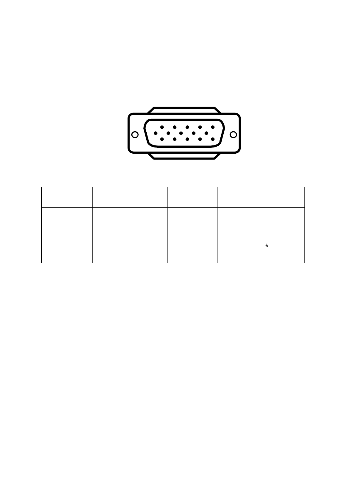
2. Connect the 15-pin color display shielded signal cable to your signal system device and lock both screws on the
connector to ensure firm grounding. The connector information is as follow:
PIN NO.
DESCRIPTION
1. RED 9. NC
2. GREEN 10. GND
3. BLUE 11. SYNC. GND
4. GND 12. SDA
5. GND 13. HORIZ. SYNC
6. GND-R 14.
7. GND-G 15. SCL
8. GND-B
3. Apply power to the display by turning the power switch to the "ON" position and allow about thirty seconds for
display tube warm-up. The Power-On indicator lights when the display is on.
4. With proper signals feed to the display, a pattern or data should appear on the screen, adjust the brightness and
contrast to the most pleasing display.
5. This monitor has power saving function following the VESA DPMS. Be sure to connect the signal cable to the PC.
6. If your 7K Series color display requires service, it must be returned with th e power cord.
1
6
11 15
5
10
15 - Pin Color Display Signal Cable
PIN NO.
DESCRIPTION
VERT. SYNC (
VCLK)
7
Page 9

4. ADJUSTMENT
4-1 ADJUSTMENT CONDITIONS AND PRECAUTIONS
1. Approximately 30 minutes should be allowed for warm up before proceeding.
2. Adjustments should be undertaken only on those necessary elements since most of them have been carefully preset
at the factory.
4-2 MAIN ADJUSTMENTS
NO. FUNCTION LOCATION DESIGNATION
1. HV ADJ PCB - MAIN VR703
2. 180V ADJ PCB - MAIN VR902
3. SCREEN ADJ FLY BACK TRANS T402
4. FOCUS ADJ FLY BACK TRANS T402
5. ABL ADJ PCB - MAIN VR701
6. SUB-BRIGHTNESS ADJ PCB - MAIN VR702
7.
FUNCTION ADJ -MENU
-UP
-DOWN PCB - MAIN SW6
-EXIT
4-3 ADJUSTMENT METHOD
1. 180V, Sub-Brightness & HV voltage adjustment:
A. Chroma-2000 Signal generator or PC equivalent set mode 1, VGA 1024X768 pattern 1.0.
B. Connect a DC Volt meter between D918 cathode and ground, then adjust VR902 to be 180VDC.
C. Connect an accurate,high impedance,HV meter between second anode lead and CRT dag grounding device. Then
adjust VR703 to be 25.0KVDC.
D. Connect a DC Volt meter between TP701(G1) and ground, Brightness set to cen ter and contrast set to max. Then
adjust VR702 to be -10 VDC.
E. Connect a 20kΩ resistor in parallel with R403 to increase the HV, the hold down circuit will operate and the
display will disappear. Then disconnect this resistor to bring the unit to normal condition.
2. Factory preset Timings Adjustment:
A. Press MENU Key to show OSD window press Up or Down Key to switch the functional controls.
B. Press the Up Key to select the "ZOOM" function, then press the MENU Key. While do not release the MENU Key
until the OSD window changed to the Factory preset window.
C. The Factory preset window contains the following func tional controls. Select one of the controls. Then press the
Up/Down Key to adjust it's value for the optimum picture.
D. Press MENU Key to Quit the OSD window. Mean while the new setting data will be saved in the memory.
E. To switches the input signal to the other Timing Mode. Please follow step C ~ D to get the optimum picture.
2
PCB - MAIN SW4
PCB - MAIN SW5
1
PCB - MAIN SW7
F. Select the "
" RETURN function and press the MENU Key, then the Factor Preset window will be returned
to the original OSD window.(user's operating condition)
G. The setting data of the CONTRAST, BRIGHTNESS, PIN-BALANCE, PARALLELOGRAM, ROTATION,
COLOR TEMPERATURE are common mode saved in the memory. Don't needed adjust it individual at every
timing Mode and save in the memory.
H
Model select: for factory only, service engineer can't changed.
8
Page 10
6500
9300
FH :68.7KH z
R
G B
G B
R
FV :85.0Hz
CONTRAST
BRIGHTNESS
H-CENTER
H-SIZE
V-CENTER
V-SIZE
ZOOM
Top corner
Bottom corner
9300
H-MOIRE REDUCE
V-MOIRE REDUCE(No use)
R-GAIN
G-GAIN
B-GAIN
R-BIAS
G-BIAS
B-BIAS
COLOR TEMPERATURE
Vs
Vc
R
G B
R
G B
TM
PINCUSHION
TRAPEZOID
PIN-BALANCE
PARALLELOGRAM
ROTATION
Sub V-size
Sub V-center
H-Convergence
V-Convergence
Exceed Frequency
Used time
6500
HS
HP
SB
BI
COLOR TEMPERATURE
DEGAUSS
OSD EXIT
RETURN
Vs Linear
Vc Linear
H-SIZE (NO use)
Max H-SIZE
Moire Disable
Super Brightness Quality
Burn In
9
Page 11
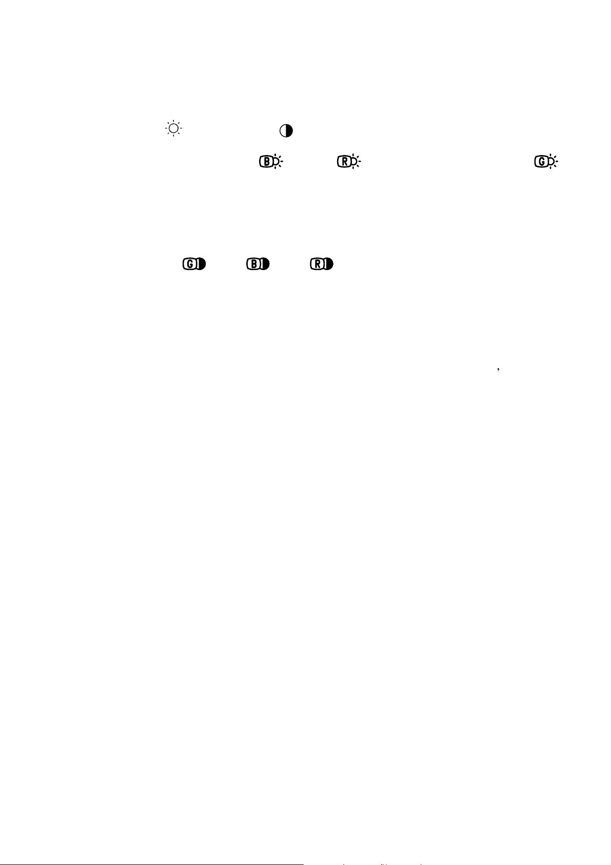
3. White Balance, Luminance adjustment:
A. Bias (Low Luminance) adjustment:
(a) Set mode 5 1024×768 Fh: 68.6KHz full white pattern.
(b) To make the adjustment condition is under the Factory preset window.
Same as step 2-C.
(c) Warm up more than 30 minutes.
(d) Brightness
Y= 0.18 ± 0.03cd/m
(e) Make the setting value of B-Bias
50DAC, then adjust FBT screen G2 VR and th e R.B. Bias individual to the color temperature x= 260 ± 10, y=
290 ± 10,Y=0.18±0.03cd/m
set to center. Contrast set to max. raster pattern, then adjust FBT screen G2 VR to make
2
.
and R-Bias to 20DAC, keep the value of G-BIAS to
2
.
(f) Select OSD function to the 9300°K and 6500°K function individually, then press the MENU Key to make the
setting data saved in the memory.
B. Gain (High light) adjustment:
(a) Set mode 5 1024×768 Fh: 68.6KHz 1/3 white area(100mmX100mm Window).
(b) Brightness set to 50DAC and set the contrast to max.
(c) Adjust G-Gain
10,Y=140 ±10cd/m
, B-Gain , R-Gain , to make color temperature x=283 ± 10, y=297 ±
2
.
C. Select OSD function to the 9300°K function, then press the MENU Key to make the setting data saved in the
memory.
D. The adjustment of 6500°K white Balance may follow step B ~ C , with the x=313 ± 10, y=329 ± 10, Y=140
±10cd/m
2
.
E. Selet “SB” Function to ON.
F. The adjustment of 9300°K(SBQ) white blance may follow B~C with the x=283±10, y=297±10,Y≥280cd/m
G. The adjustment of 6500
o
K (SBQ) white Balance, May follow B~C with the x=313±10,y=329±10 Y≥260cd/m2 .
H. Select “SB” function to OFF and Exit factory preset model.
I. Full white luminance:
(a) Set mode 2 640×480 Fh: 68.6KHz full white pattern.
(b) Image Size : H:310±4mm V:232.5±4mm.
(c) Brightness set to 50 DAC and set the contrast to max.
(d) Adjust VR701 to the luminance at 105±5cd/m
2
.
4. Focus Adjustment:
A. Set mode5 1024×768 Fh: 68.6KHz with character full page.
B. Adjust brightness to center and contrast to max.
C. Then adjust focus VR1 to a fine vertical line.
D. Adjust focus VR2 to a fine horizontal line.
E. Repeat step C & D..
5. Purity Adjustment
A. Be sure that the display is not being exposed to any external magnetic fields.
B. Ensure that the spacing between the Purity, Convergence, Magnet, (PCM), assembly and the CRT stem is
29mm .(See below diagram)
C. Produce a complete, red pattern on the display. Adju st the purity magnet rings on the PCM assembly to obtain a
complete field of the color red. This is done by moving the two tabs in such a manner that they advance in an
opposite direction but at the same time to obtain the same angle between the two tabs, which should be
approximately 180'.
D. Check the complete blue and complete green patterns to observe their respective color purity. Make minor
adjustments if needed.
2
.
10
Page 12

RELATIVE PLACEMENT OF TYPICAL COMPONENTS
Purity Magnets
6-pole Convergence Magnets
4-pole Convergence Magnets
Deflection Yoke
6. Convergence adjustment
A. Produce a magenta crosshatch on the display.
B. Adjust the focus for the best overall focus on the display.
Also adjust the brightness to the desired condition.
C. Vertical red and blue lines are converged by varying the angle between the two tabs of the 4 pole magnets on the
PCM assembly. (See above diagrams)
D. Horizontal red and blue lines are converged by varying the two tabs together, keeping the angle between them
constant.
E. Produce a white crosshatch pattern on the display.
F. Vertical green and magenta lines are converged by varying the angle between the two tabs of the 6-pole magnets.
G. Horizontal green and magenta lines are converged by varying the two tabs together, keeping the angle between
them constant.
5. CIRCUIT DESCRIPTION
5-1 MICRO CONTROLLER CIRCUIT
MICRO Controller
The IC101 contains a 6502 8-bit CPU core, 256 bytes of RAM, 16K bytes of ROM,14 channel 8 bit PWM D/A
converters, 2 channel A/D converters for key detection, one 8 bit pre-loadable base timer, internal H-sync and V-sync
signals processor providing mode detection, watch- dog timer preventing system from abnormal operation, and an I
interface.
2
C bus
H/V sync signals processor
The functions of the sync processor include polarity detection, H-SYNC & V-SYNC signals counting, Programmable
SYNC signals output, free running signal generator,and composite sync separation Pin41/Pin42 are for the H-SYNC and
V-SYNC input, Pin33/Pin34 will output the same signal as input sync signal without delay, an d the polarity are setting in
the positive. When no signal input, the Pin33 will output a 61HZ V-SYNC free run signal. The Pin34 will output a
62.5KHz H-SYNC free run signal. for the monitor testing use.
11
Page 13

On Screen Display Controller
The IC802 on video board is designed for display the built-in characters or fonts onto monitor screen. The display
operation is by transforming data and control information from micro controller to RAM through a serial data interface.
Pin2 is used to control the internal oscillator frequency by DC voltage input from external low pass filter (R830, C817,
R833) and filter (R832, C818) is used to regulate the appropriate bias current for internal oscillator the resonate at specific
dot frequency.
Pin5 is input the horizontal fly back pulse, for PLL generator tracking.
Pin6 is left floating, I
2
C bus is enabled. Otherwise the SPI bus is enabled.
Pin7 the external data transfer through this pin to internal display registers and control registers
Pin8 the clock-input pin is used to synchronize the data transfer.
Pin10 is input the vertical flyback pulse for synchronizing the vertical position.
Pin12 is output a blanking signal to cut off external R.G.B signals of VGA while this chip is displayin g characters or
windows.
Pin13, Pin14, Pin15 is used to output the OSD (B.G.R) video signal.
5-2 DEFLECTION CIRCUIT
The deflection circuit is achieved by a high performance and efficient solution IC401 (TDA4856) for this monitor. The
concept is fully DC controllable and can be used in applications with a micro-controller solutions.
The TDA 4856 provides sync. Processing with full auto sync. capability, a flexible SMPS block and an extensiv e set of
geometry control facilities. Further the IC generates the drive waveforms for DC coupled vertical boosters to the TDA
4887PS [ref Page-28].
Horizontal Oscillator
The oscillator is of the relaxation type and requires a capacitor of 10nF C413 at pin 29. The maximum oscillator
frequency is determined by a resistor R426 form pin 28 to ground. A resistor R425 from pin27 to pin28 defines the
frequency range.
PLL 1 Phase Detector
The phase detector is a standard one using switched current sources. It compares the middle of H-sync. with a fixed point
on the oscillator saw-tooth voltage. The PLL loop filter C411, R424, C412 is connected to Pin26.
PLL2 Phase Detector
This phase detector is similar to the PLL1 detector and compares the line flyback pulse at pin 1 with the oscillator sawtooth voltage. The PLL2 detector thus compensates for the delay in the external H-deflection circuit by adjusting the
phase of the HDRV output pulses. The phase between H-flyback and H-sync can be controlled at pin30.
X-ray Protection
The X-ray protection input pin2 provides a voltage detector with a precise threshold. If the voltage exceeds this threshold
for a certain time, an internal latch switches the whole IC into protection mode. In this mode several pins are forced into
defined states:
Pin8 (HDRV) is floating
Pin6 (BDRV) is floating
Pin12, 13 ( VOUT 1, 2) are floating
Pin16 (CLBL) provides a continuous blanking signal.
Vertical Oscillator
The vertical free –running frequency is determined by the resistor R602 at pin23 and capacitor C602 at pin24. Usually the
free-running frequency should be lower than the minimum trigger frequency.
5-3 PFC CIRCUIT
Between rectifier and loading, it is connected a DC-DC switch transformer .Through input current Ii wave following AC
input sinusoid voltage wave, Ii may approach sine wave, and input THD may less than 5%,power factor may improve
more 0.9. IC905 is used for power factor correction . Q910 is DC-DC power switch transistor, and R955
R956 is used as
divider.
12
Page 14

5-4 TRANSISTOR & DIODE CIRCUIT
LOCATION
FUNCTION AL DESCRIPTION
D101 For C103 Discharge
Q101 For LED Indicator Control
D411 Speed up for Q410
D412 Damping Diode
Q405 HDRV Mute Control
Q409 Horizontal Driver
Q410 Horizontal Out Put
Q413 Horizontal Linearity Correction Control
Q415~ Q419 Horizontal S-Correction Control
Q429~ Q433 Horizontal S-Correction Control
D705 Buffer Diode
D701 Rectifier for 250V Supply
D702 Protection Diode for Q701
D703,D704 Rectifier for -200V Supply
Q707 Picture Mute Control AMP
Q705, Q706 Brightness Control CKT
Q701 Vertical Dynamic Focus Control AMP
BD901 Bridge Rectifier for AC Source
D909 Rectifier for Start Power Supply
D907 Clip Diode for Snubber CKT
D906 IC901 VCC Supply
D910 Speed UP for Q901
D911 Synchronous Trigger for Power Supply
D912,D913,D918 Rectifier for 180V Output Voltage Supply
D916,D917,D924 Rectifier for 6.5V,16V,-10V Output Voltage Supply
D914 , D901 Rectifier for 80V Output Voltage Supply
D409, D410 Raster Position Control
D905 Clip Diode for Snuffer Pulse
ZD901 Protection Diode
ZD902 Protection Diode
ZD903 Protection Diode
13
Page 15

LOCATION
FUNCTION AL DESCRIPTION
Q901 MOS FET for Switching Power Control
Q904 Start up CKT for IC901
Q912, Q913 To Turn 6.3V Supply Off when the Off Mode is Required
Q908, Q909 To Turn 16V Supply Off when the Off or Suspend Mode is Required
Q408 MOS FET for B+ Control
Q406, Q407 Push Pull Driver for Q408
D856 ~ D858 DC Restoration for CRT Bias Adjustment
D850 , D852,D854 Protection Diode for Q801, Q802, Q803.
Q850 ~ Q852 DC Restoration for CRT Bias Adjustment
14
Page 16
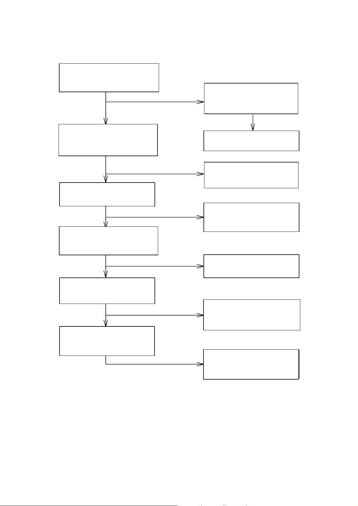
6.TROUBLE SHOOTING CHART
6-1 NO RASTER, CRT RELATIVE CIRCUIT PROBLEMS
CHECK MAIN PCB POWER SUPPLY
POWER SUPPLY 180V,16V,80V
60.5V, 14.5V, 80V
CHECK MAIN PCB
NG
OK
CHECK THE HIGE VOLTAGE OF
CHECK THE HIGE VOLTAGE
CRT ABOUT 25±0.3KV OR Q409
OF CRT ABOUT 25.5 ~ 26.5KV
DRAIN PIN VOLTAGE WAVE
OK
CHECK THE VOLTAGE OF CRT
HEATER ABOUT 6.3V
OK
NG
NG
CHECK SCREEN VOLTAGE
CHECK SCREEN VOLTAGE ABOUT
ABOUT 500V TO 800V
400V TO 700V
LESS THAN 300V
OK
CHECK POWER SAVING CIRCUIT,
H-SYNC, V-SYNC SIGNAL
OK
REFER ITEM S.M.P.S.
CHECK FAILSAFE CKT IC401
PIN 2 RELATIVE CKT.
CHECK CRT'S HEATER RELATIVE
CIRCUIT
CHECK FBT
BRIGHTNESS SET TO MAX.
THEN CHECK CRT G1 VOLTAGE
CHECK BRIGHTNESS CIRCUIT
NG
OK
CHECK VOLTAGE OF THE CRT
CATHODE ABOUT 60V TO 70V
NG
CHECK BRIGHTNESS CIRCUIT
Q705,Q706, RELATIVE CKT.
Q703, Q706, Q707 RELATIVE CKT.
REFER ITEM 6-2 “ABNORMAL
REFER ITEM 8-2
"ABNORMAL DISPLAY"
DISPLAY”
15
Page 17
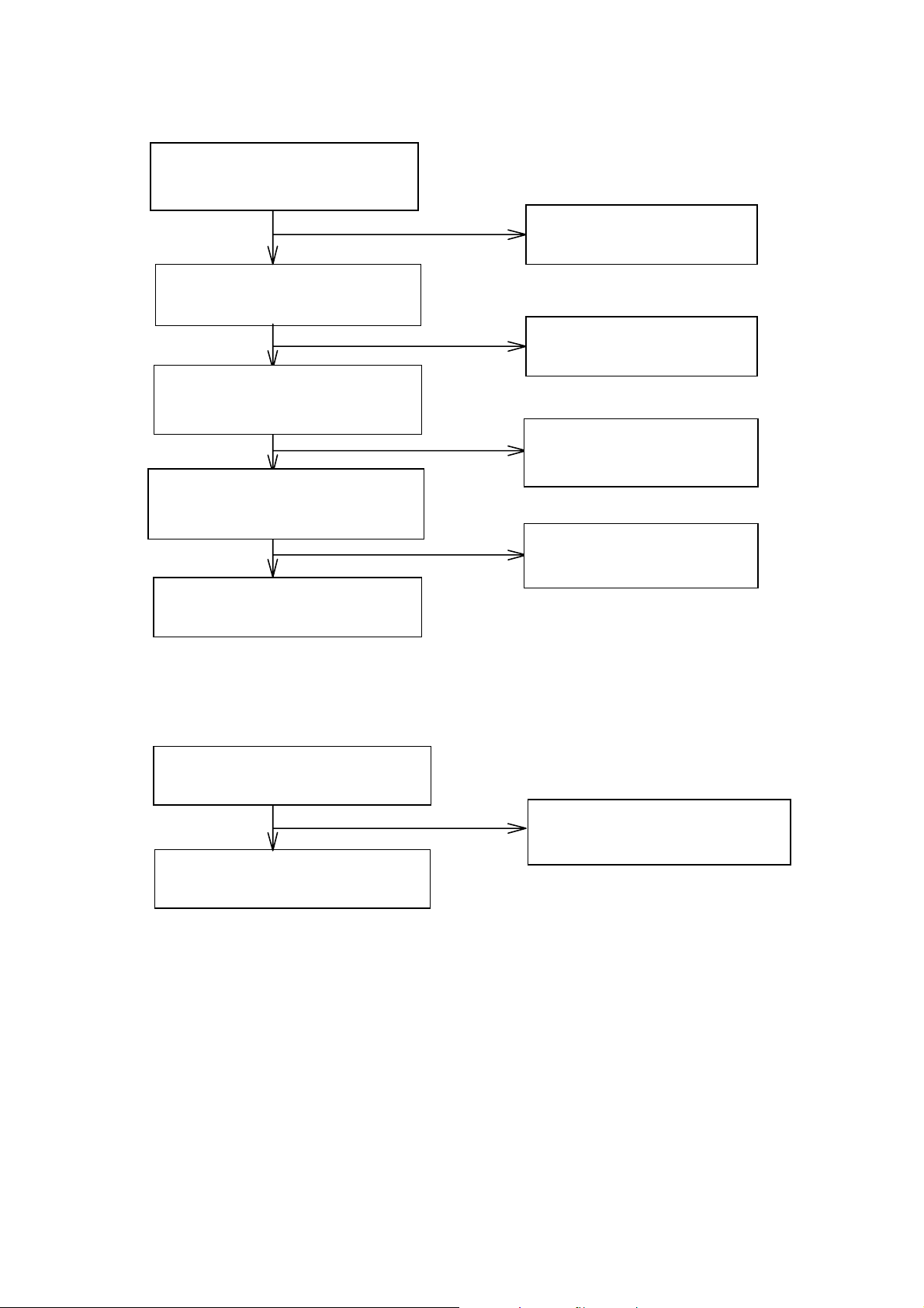
2.ABNORMAL VIDEO LEVEL ON SCREEN
HECK THE VOLTAGE OF IC801
CHECK THE VOLTAGE OF IC801
PIN 6, 9, 22 ABOUT 12V
PIN7,15,18,21
NG
OK
CHECK THE SIGNAL INPUT OF R.G.B.
ABOUT 0.7Vpp
OK
CHECK IC801 PIN5
CHECK IC801 PIN 15 CLAMP PULSE
CLAMP PULSE PI
PIN 16 BLANK PULSE
CHECK THE VIDEO OUTPUT OF
CHECK THE VIDEO OUTPUT OF IC801
PIN 18, 20, 23 ABOUT 4Vpp,
CONTRAST SET MAX.
R.G.B. APPROACH STANDARD
11 BLANK PULSE
NG
OK
IC801 PIN16,19,22 ABOUT
4Vpp,CONTRAST SET MAX.
NG
OK
CHECK 12V RELATIVE
CIRCUIT
CHECK SIGNAL CABLE OR
INTERFACE CARD.
CHECK THE IC105 RELATIVE CIRCUIT
IC401 PIN16 OUTPUT
OR IC401 PIN 16 OUTPUT
CHECK IC801 PIN 13 ABOUT 4V
PIN 26, 27, 28 ABOUT 4V OR
CHECK IC801 PIN24 ABOUT
CHECK Q801 AND RELATIVE CKT
3. ABNORMAL DDC (PLUG & PLAY)
CHECK IC101 PIN 5 VOLTAGE ABOUT 5V
NG
OK
CHECK SIGNAL CABLE
OR H802 PIN 3, 4 DATA OUTPUT
CHECK Q102 GOOD OR FAIL
16
Page 18
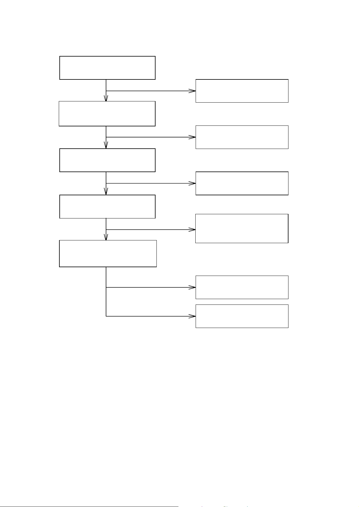
6-2 ABNORMAL DISPLAY
1.NO SIGNAL ON SCREEN
CHECK VIDEO IC801 VCC ABOUT 12V
NG
OK
CHECK THEOUTPUTVOLTAGE
CHECK THE OUTPUT VOLTAGE
OF IC801 PIN16,19,22 ABOUT 3Vpp
OF IC801 PIN 18, 20, 23 ABOUT 3Vpp
NG
OK
CHECK THE B+ VOLTAGE OF
VIDEO PCB ABOUT 80V
NG
OK
CHECK THE VOLTAGE OF CRT
CATHODE ABOUT 40Vpp
NG
OK
CHECK THE VOLTAGE OF FBT
CHECK THE VOLTAGE OF FBT SCREEN
SCREEN ABOUT 500V TO 800V
ABOUT 400V TO 700V
CHECK THE 12V PIN
OF P802 CONNECTOR
CHECK THE RELATIVE CIRCUIT
OF IC801
CHECK THE 80V RELATIVE CIRCUIT
OF SMPS ON MAIN PCB
CHECK THE IC803 PIN1,2,3
CHECKTHE VQ802 ~ Q807
OUTPUT RELATIVE CIRCUIT
RELATIVE CIRCUIT
LESS THAN 500V
LESS THAN 400V
EXCEED 700V
CHECK FBT RELATIVE
CIRCUIT
CHECK FBT & CRT RELATIVE CIRCUIT
OR REFER ITEM 7-1
17
Page 19

6-3 NO BLANKING
CHECK THE RELATIVE
CIRCUIT OF BLANKING
CHECK THE RELATIVE CIRCUIT OF
NG
OK
CHECK THE RELATIVE CIRCUIT
D424,R497,ZD404 ON MAIN PCB
OF C433, D410, R635, R636, IC105
ON MAIN PCB
CHECK IC801 PIN11 VIDEO PCB,CHECK
CHECK IC801 PIN 16 ON VIDEO PCB,
G1 RELATIVE CIRCUIT
CHECK G1 RELATIVE CIRCUIT
Q702,Q703,Q704,C711,C712
Q705, R718, C707 ON MAIN PCB
6-4 HOR./OSC/DEF/HV CIRCUIT FAULT
1. NO RASTER (DISCONNECT WITH SIGNAL CABLE)
CHECK IC401 PIN 10 ABOUT 11.5 VDC
NG
OK
CHECK IC401 PIN 8 WAVE FORM
ABOUT 10Vpp
NG
OK
CHECK THE DRAIN VOLTAGE OF
CHECK THE COLLECTOR VOLTAGE
Q409 ABOUT 40Vpp
OF Q402 ABOUT 40Vpp
NG
OK
CHECK THE COLLECTOR
CHECK THE COLLECTOR VOLTAGE
VOLTAGE OF Q410 ABOUT 900Vpp
OF Q403 ABOUT 1100Vpp AT FH:31KHz
AT FH:31KHZ
NG
CHECK IC401 PIN 10 RELATIVE CIRCUIT
CHECK IC401 PIN 26 ~ 31
RELATIVE CIRCUIT
CHECK Q409,T401 RELATIVE
CHECK Q402, T401
CIRCUIT
RELATIVE CIRCUIT
CHECK Q410,D412,C424,H-DY
CHECK T401, T402, Q402, Q403,
Q408,R449
D408, C418, C419, H-DY
18
Page 20

6-5 ABNORMAL HORIZONTAL DEFLECTION
N
1. ABNORMAL HORIZONTAL WIDTH OF VIDEO
READJUST H-WIDTH FUNCTION
NG
OK
CHECK FBT B+ VOLTAGE
CHECK FBT B+ VOLTAGE AT Q408
GATE
ABOUT 60.0V AT FH=31KHz
G
CHECK THE HV OF
CHECK THE HV OF CRT ABOUT
25KV
CRT ABOUT 26KV
CHECK THE RELATIVE CIRCUIT
CHECK THE RELATIE CIRCUIT OF
Q409
OF Q404, Q405, & Q406
CHECK THE RELATIVE
CHECK THE RELATIVE CIRCUIT OF
SMPS. Q408,IC401 PIN 4
CIRCUIT OF SMPS.
Q911, Q912, Q914, Q915 &
IC401 PIN 4, 5, 6, VR 902
5 6 ,VR902
2. ABNORMAL HORIZONTAL RASTER CENTER
CHECK T903, D926, D927, R964, R968
CHECK T405,D409,D410,R436,P401 AND
JUMPER
P403 AND JUMPER
3. ABNORMAL HORIZONTAL VIDEO CENTER
CHECK IC101 PIN 9, 10, IC401 PIN 18, 19
CHECK IC101 PIN10,11 IC401 PIN18,19
4. ABNORMAL HORIZONTAL LINEARITY
CHECK L401, Q407, R447, C448
CHECK T402,Q413,R448,C428 AND IC101 PIN19~23
AND IC101 PIN 20, 21, 22, 23
CS SWITCHER Q429~Q433 Q415~Q419
CS SWITCHER IC403, Q410, Q411, Q420
19
Page 21

6-6 ABNORMAL VERTICAL SCANNING
1. ABNORMAL VERTICAL SIZE
READJUST V-SIZE FUNCTION
READJUST V-SIZE FUNCTION VALUE
VALUE CHECK THE IC601
CHECK THE IC601 PIN 7 ABOUT 40V
PIN3,2 ABOUT 13V
NG
OK
CHECK VERT. OSC CIRCUIT
NG
OK
CHECK IC601 PIN5 OUTPUT
CHECK IC601 PIN 6 OUTPUT ABOUT
VOLTAGE WAVE
38Vpp
NG
CHECK D601,D602,R606
CHECK ZD601, ZD602 R626 & SMPS
R609& SMPS RELATIVE
RELATIVE CIRCUIT
CIRCUIT
CHECK IC401 PIN 22, 23, 24
CHECK IC401 PIN 12, 13
RELATIVE CIRCUIT
2. VERTICAL CENTER
READJUST V-CENTER
NG
CHECK IC101 PIN10,11 IC401
CHECK IC101 PIN 9, 10
PIN18,19
IC401 PIN 18, 19
6-7 SIDE-PIN CUSHION DISTORTION
READJUST SIDEPIN
READJUST FOCUS CONTROL
NG
CHECK IC401, Q404, Q405, Q406
CHECK IC401 RELATIVE CKT
RELATIVE CKT.
6-8 POOR FOCUS
NG CHECK FOCUS CONTROL UNIT, FOCUS
LEAD WIRE, CRT SOCKET & CRT
20
Page 22

6-10 POWER SUPPLY TROUBLE SHOOTING CHART
BEFORE CHECK SW.REG. PLEASE REFER TO THE POWER SUPPLY BLOCK DIAGRAM
POWER SUPPLY OUTPUT: (A) CONSTANT OUTPUT : 6.5V, 16V, 80V, 180 V, -10V
BEAD SET
ABNORMAL VARIABLE OUTPUT
CHECK AC LINE
VOLT 120V OR 220V
NG
OK
CHECK LINE RECTIFIED
& SMOOTHED VOLT
NG
OK
CHECK START C.K.T
CHECK START C.K.T
D909, Q904, R922, R925
ZD902,Q904,D909,R908
NG
OK
CHECK T901 O/P
CHECK F901, SW901
CHECK BRIDGE
RECTIFIED CIRCUIT
CHECK POWER SAVING
C.K.T(OFF-MODE)
MAKE SURE THAT
THE VARIABLE
OUTPUT IS NOT SHORTED
NO
YES
CHECK THE C934
VOLTAGE 55V
NG
OK
CHECK Q911
NG
OK
CHECK IC401
PIN 4, 5, 6, B+ DRIVER
CHECK D919
Q911 FAILURE
CHECK IC901
CHECK Q901
OK
OK
NG
NG
CHECK 180V,80V,
CHECK 80V, 55V, 14.5V
16V, 6.5V
6.3V CIRCUIT
CIRCUIT
IC901 FAILURE
NG
CHECK Q901
CHECK Q912, Q914, Q915
OK
21
Page 23

7. MECHANICAL OF CABINET FRONT DIS-ASSEMBLY
22
Page 24

8. PARTS LIST OF CABINET
PARTS LIST OF CABINET
LOCATION A791V-1C SPECIFIATION REMARK
CMA791VNC CHASSIS
1A 503- 5T- 47 SCREW
5A 38- 8 RUBBER WASHER
11A 112-500 WIRE MOUNT
11A 115- 1 FBT CLIP
12A 385- 1 RUBBER FOOT
19A 403- 7 STEEL
19A 506- 5 SPRING
33A4020- Y- A S.C.CAP
33A4123- Y- A POWER KNOB
33A4125- 1 LED LENS
33A4260- Y- A KEY PAD
33A6911- 1 CRT SUPPORT
40A 153-517 CRT WARNINGL LABEL
40A 154-501- 1 HI-POT GND LABEL
40A 581- 26-704 LABEL
40A 581-624-10A H/V LABEL
40A 581-695- 1A SERIAL LABEL
40A 581-695- 2A LABEL
40A 581-695- 3A JAPAN LABEL
40A2048-695- 5A ID LABEL
41A 68-508- A CARD
41A 586-695- 2A MANUAL
44A3241- 1 EPS
44A3241- 2 EPS
44A3241- 3 CARTON
45A 76- 20- RN PE BAG
45A 76- 28- RN pe bag
45A 76- 34- RN PE BAG
45A 77-500 BARCODE RIBBON
45A 77-501 BARCODE RIBBON
85A 576-501 CRPC SHIELD
85A 577-505 SHIELD CASE
85A6020- 2 Grounded plate
89A502A-12N- YH POWER CORD
95A 91-205-688 WARE
95A8013- 2 CONNECTOR
B1A1035- 10-128 SCREW
M1A1130- 8-128 SCREW
Q1A 340- 16-128 SCREW
34A 741- Y- L BASE
34A 806- Y- A REAR COVER
34A 824- Y- L SWIVEL
34A 860- Y- A FRONT PANEL
750A1697- 57- KA DEG.COIL
750A5726-2AV MITSUBISHI 17"FLAT
23
Page 25

PARTS LIST OF CHAS
LOCATION CMA791VN SPECIFICATION REMARK
AMA791VNC MAIN BOARD
CRA791VNC CRT BOARD
1A 421- 4-128 SCREW
9A 203- 9 PIN NR901
11A 141- 1 PCB SUPPORT
15A5640- 1- A AL GND LUG
15A5659-500- 2 Rear Bracket
40A 581- 26-702 FAIL-SAFE LABEL
40A 581-624- 2A CHASSIS LABEL
71A 100- 12 FERRITE CORE
89A174A-5DB- GR SIGNAL CABLE
95A 900- 12 HARNESS
95A 900-511 WIRE HARNESS
B1A1040- 10-128 SCREW FBT
D1A1140- 7-128 SCREW
M1A1140- 6-128 SCREW 15A5059
705A791A-C56-01A IC601 ASS'Y
705A791A-C57-01N Q901 ASS'Y
705A791A-C57-02B Q408 ASS'Y
705A791A-C57-02C Q410/Q427/D412 ASS'Y
705A791A-C87-01C AC IN SOCKET
705A791S-C56-01S IC904 ASS'Y
705A791V-C57- 05 Q432 ASS'Y
705A791V-C57- 06 Q431 ASS'Y
705A791V-C57-03C Q428 ASS'Y
750A5726-2AV-A7C 17" MPRII ASS'Y
750A5726-2AV-HA7 17" TCO ASS'Y
AA 95A 205- 69-062 WIRE HARNESS
AS1 95A205T- 30-06A Wire Harness Safety GND to Case
BD901 93A 50-460- T TS4B05G
C407 67A 309-471- 3T 470UF +-20% 16V
C416 64A178J-474- 0T CL21X. 0.47UF 50V +-5%
C424 63A210J-472-8FK 4700PF 2000V
C426 65A517K-103- 5A 10000PF/500V +-10% Y5P
C431 63A210J-683-2CC 0.068UF 250V
C433 63A210J-154-2CM 0.15UF/250V
C435 63A210J-304-2CM 0.3UF 250V PMH
C437 63A210J-754-2DH MPS 0.75UF 250V +-5%
C439 63A210J-754-2DH MPS 0.75UF 250V +-5%
C440 64A178J-104- 0T CL21X0.1UF 50V +-5%
C442 63A210J-224-3CJ 0.22UF 400V 15A
C443 67A 305-479-12T 4.7UF +-20% 250V
C449 63A210J-152-8CB 1500PF 2KV PMS
C450 65A 1K-471- 2A 470PF +-10% 1KV
C452 65A517K-100- 1A NPO 10PF 500V +-10%
C453 67A 309-470- 12 47UF -20% 250V
C454 67A 309-470- 12 47UF -20% 250V
C464 67A 305-479-12T 4.7UF +-20% 250V
C606 67A 309-471- 3T 470UF +-20% 16V
C610 67A 305-102- 3 1000 UF +-20% 16V
C703 65A517K-103- 5A 10000PF/500V +-10% Y5P
24
Page 26

LOCATION CMA791VN SPECIFICATION REMARK
C711 67A 309-100- 11 10UF +-20% 200V
C728 67A 305-101- 9 100UF +-20% 100V
C901 63A 107-224- H INTERFERENCE SUPPRESSORS
C902
C903 65A305M-332-2B2 3300PF 250VAC/400VAC
C904
C905 65A305M-472-2B2 4700PF +-20% 400VAC PY17
65A305M-332-2B2 3300PF 250VAC/400VAC
67A 30-151-15D 150UF +-20% 450V HEC
C907 65A 2M-103- 3B 0.01UF 2KV 20% Z5U
C921 67A 305-101-10J 100UF +-20% 160V JAMICON
C922 67A 305-101-10J 100UF +-20% 160V JAMICON
C923 67A 305-101- 9 100UF +-20% 100V
C924 67A 305-101- 9 100UF +-20% 100V
C927 67A 305-102- 3 1000 UF +-20% 16V
C932 67A 305-471- 4 470UF +-20% 25V
C933 67A 305-471- 4 470UF +-20% 25V
C936 67A 309-471- 3 470UF +-20% 16V
C944 63A 107-334-10S 0.33UF 275VAC PITCH=1
C950 63A210J-684-4MC 0.68UF 630V
C953 65A 1M-103- 3A 0.01UF 1K Z5U
CN902 33A3074- 1 2P PLUG
D421 93A2100- 1-52T BYM26E/PHILIPS
D423 93A1002- 1W-52T 1N5817
D425 93A1060- 6-52T F R D BYV26C
D908 93A3060-501-52T 31GF6
D912 93A2060- 1-52T FRD BYM26C
D913 93A2060- 1-52T FRD BYM26C
D916 93A3020- 13-52T EGP30D
D917 93A3020- 12 RL-3 SANKEN
D918 93A2060- 1-52T FRD BYM26C
D924 93A3020- 8T RG-4Z
DF421 71A 55- 2 FERRITE BEAD CORE FOR D421 E PIN
DF425 71A 55- 2 FERRITE BEAD CORE FORD425 E PIN
DF908 71A 55- 2 FERRITE BEAD
DF912 71A 55- 2 FERRITE BEAD
DF916 71A 55- 2 FERRITE BEAD
DF924 71A 55- 2 FERRITE BEAD CORE FOR D924 E PIN
F 71A 100- 8 FERRITE CORE
F901 84A 33- 10 FUSE CLIP
F901 84A 7H-400- SL FUSE 4A 250V LF-618 004
FB402 71A 55-19R FERRITE BEAD
FB403 71A 55-19R FERRITE BEAD
FF 95A 205- 50-062 WIRE HARNESS
GND6 9A 203- 8 BRASS PIN
H802 95A8013- 12-506 WIRE&HARNESS
H803 95A8013- 6-14A WIRE & HOUSING ASS'Y
HS2 95A205T- 30-04A Wire Harness
IC101 56A1125-100- X NT68P61AU
IC102 56A1133- 14 AT24C08-10PC
IC201 56A 192- 6 LM358N ST
IC401 56A 552- 2 TDA4841PS/PHILIPS
IC402 56A 580- 1 TC4538BP
IC701 56A 192- 6 LM358N ST
IC901 56A 379- 12 8PIN IC UC3842AM/LIN
IC903
56A 139- 3 PC123FY2 BY SHARP
25
Page 27

LOCATION CMA791VN SPECIFICATION REMARK
IC905 56A 538- 5 MC33260P
IC906 56A 192- 6 LM358N ST
IC907 56A 133- 5- ST VOLT REG.L7805CV/SGS-THO
J137 95A 90- 23 TIN COATED FOR X101
L401 73A 253-106- L CHOKE COIL
L402 73A 253-111- T CHOKE COIL
L901
L902 73A 174- 2- SA 25MH FILTER
73A 174- 2- SA 25MH FILTER
L903 73A 259- 2 30UH +/-15%
L904 73A 259- 2 30UH +/-15%
L905 73A 259- 2 30UH +/-15%
L907 73A 259- 2 30UH +/-15%
L908
73A 253-121- T 125MH
LED1 81A 10- 6- BH LED/HOLDER ASSEMGLT
NR601 61A 58-101- UT NTCR100OHM+-15%3100K UPP
NR901 61A 58- 9U NTCR 10OHM+-20% 5A UPPER
P201 33A3278- 2 2P PLUG B2B-XHA/JST
P202 33A3278- 2 2P PLUG B2B-XHA/JST
P401 33A8009- 3 3 PIN PLUG
P402 33A3192- 4 4P PLUG
P701 33A3278- 2 2P PLUG B2B-XHA/JST
PR901 61A 52-459- MT PTCR4.5OHM +30%-20%220V
Q409 57A 600-504 POWER MOSFET IRF634A FAI
Q429 57A 600- 8 MOS FET IRF630 I.R
Q430 57A 600- 8 MOS FET IRF630 I.R
Q433 57A 600- 8 MOS FET IRF630 I.R
Q908 57A 728- 3 HSB772P/HSB772E HI-SINCE
Q912 57A 728- 3 HSB772P/HSB772E HI-SINCE
R407 61A152M-100- 64 MOFR 10 OHM+-5% 2W
R432 61A 208-271- 64 MOFR 270 OHM +-5% 1W
R435 61A152M-109- 64 MOFR 1 OHM +-5% 2W
R436 61A152M-120- 64 MOFR 12 OHM +-5% 2W
R439 61A153M-121- 59 MOFR 120 OHM+-5% 3W
R440 61A152M-272- 64 MOFR 2.7KOHM+-5% 2W
R441 61A153M-209- 59 MOFR 2 OHM+-5% 3W
R442 61A153M-209- 59 MOFR 2 OHM+-5% 3W
R449 61A 301-109- 64 FUSER 1OHM +-5% 1/2W
R453 61A152M-330- 64 MOFR 33 OHM+-5% 2W
R467 61A153M-101- 59 MOFR 100 OHM +-5% 3W
R482 61A152M-470- 64 MOFR 47 OHM+-5% 2W
R483 61A153M-121- 59 MOFR 120 OHM+-5% 3W
R498 61A153M-121- 59 MOFR 120 OHM+-5% 3W
R606 61A 208-479- 64 MOFR 4.7 OHM +-5% 1W
R609 61A 208-479- 64 MOFR 4.7 OHM +-5% 1W
R614 61A 208-181- 64 MOFR 180 OHM +-5% 1W
R615 61A 208-828- 64 MOFR 0.82OHM +-5% 1W
R705 61A152M-101- 64 MOFR 100OHM+-5% 2W
R743 61A 208-101- 64 MOFR 100OHM+-5% 1W
R907 61A212Y-474-52T MGFR 470KOHM +-5% 1/2W
R914 61A 20J-333-BE1 CEMENTR 33K OHM +- 5%
R919 61A152M-228- 64 MOFR 0.22 OHM+-5% 2W
R927 61A 208-390- 64 MOFR 39 OHM +-5% 1W
26
Page 28

LOCATION CMA791VN SPECIFICATION REMARK
R929 61A175L-102-52T CFR 1K OHM +-5% 1/2W
R938 61A 208-114- 64 MOFR 110K OHM +-5% 1W
R944 61A 208-333- 64 MOFR 33K OHM +-5% 1W
R953 61A 20K-478-GE1 CEMENTR 0.47OHM +-10% 5W
R958 61A 208-390- 64 MOFR 39 OHM +-5% 1W
RA101 61A 124-472- 6 AR 6P5R 4.7KOHM +-5% 1/8
RA102 61A 124-472- 12 AR 12P11R 4.7KOHM +-5% 1/8
RA103 61A 124-472- 10 AR 10P9R 4.7KOHM +-5% 1/8
RA104
RY901 77A 260- 5- 4 RELAY
61A 124-472- 6 AR 6P5R 4.7KOHM +-5% 1/8
SG701 62A 10- 16- W SPARK GAP 1KV+500-100V C
SS1 95A205T- 30-06A Wire Harness Signal Screw to Case
SW4 77A 602- 1- CJ TACT SWITCH TSVB-2
SW5 77A 602- 1- CJ TACT SWITCH TSVB-2
SW6 77A 602- 1- CJ TACT SWITCH TSVB-2
SW7
SW901 77A411A- 2- S PUSH SWITCH
77A 602- 1- CJ TACT SWITCH TSVB-2
T401 79A 167-114- H DRIVER TRANSFORMER
T402 73A 147-123- T LINEARITY COIL LINEARITY
T403 79A9110- 2- L FBT
T404 79A 167-112- LA DRIVER TRANSFORMER
T405 79A 167-122- L DRIVR X'FMR
T901
T902 73A 174- 18- H
80AA791- 1- TA CONVERTER
1:1 TRANSFORMOR
TP701 9A 211- 2 PIN 1.2X15MM
VR701 75A 335-203 CFVR 20K OHM +-20%
VR702 75A 335-204 CFVR 200K OHM +-20%
VR703 75A 335-303 CFVR 30K OHM +-20%
VR902 75A 334-303 CFVR 30K OHM +-20%
X101 93A 22- 22- PT HC-49U 8MHz Crystal
ZD401 93A 39- 43-52T 1N4742A/MOTOROLA
PARTS LIST OF MAIN PC BOARD
LOCATION AMA791VN SPECIFICATION REMARK
6A 31- 4 BRASS
6A 31-501 BRASS
715A 882- 2 MAIN BOARD
C101 65A 450-104- 7T 0.1UF +80-20% 50V Y5V
C102 67A 309-101- 3T 100UF +-20% 16V
C103 67A 309-330- 3T 33UF +-20% 16V
C104 65A 442-330-13T 33PF +-5% NPO 50V
C105 65A 442-330-13T 33PF +-5% NPO 50V
C106 65A 444-472-13T 4700PF +-10% Z5P 50V
C111 67A 309-229- 7T 2.2UF +-20% 50V
C112 67A 309-229- 7T 2.2UF +-20% 50V
C121 67A 309-330- 3T 33UF +-20% 16V
C130 65A 444-103- 5T 0.01 UF 10% 50V Y5P
C201 67A 309-101- 3T 100UF +-20% 16V
C202 65A 450-104- 7T 0.1UF +80-20% 50V Y5V
C203 67A 309-100- 7T 10UF +-20% 50V
27
Page 29

LOCATION AMA791VN SPECIFICATION REMARK
C204 67A 309-101- 3T 100UF +-20% 16V
C205 65A 450-104- 7T 0.1UF +80-20% 50V Y5V
C206 67A 309-100- 7T 10UF +-20% 50V
C207 64A176J-152- 1T 1500PF 100V
C208 64A701J-224-0AT 0.22uF/50V +-5%
C402
65A 450-104- 7T 0.1UF +80-20% 50V Y5V
C403 67A 309-220- 7T 22UF +-20% 50V
C404 64A176J-103- 1T 0.01UF 5% 100V
C405 65A 442-101-13T 100PF +-5% NPO 50V
C406 64A176J-222- 1T 0.0022UF 5% 100V
C408 67A 305-229- 7T 2.2UF +-20% 50V
C409 65A 442-101-13T 100PF +-5% NPO 50V
C410 65A 442-470-13T 47PF +-5% NPO 50V
C411 64A176J-474- 1T 0.47UF +-5% 100V
C412 64A176J-103- 1T 0.01UF 5% 100V
C413 64A176J-103- 1T 0.01UF 5% 100V
C414 64A176J-562- 1T 5600PF +-5% 100V
C415 65A 444-101- 5T 100 PF 10% 50V Y5P
C417 65A 442-101-13T 100PF +-5% NPO 50V
C418 67A 309-101- 4T 100UF +-20% 25V
C419 67A 309-101- 4T 100UF +-20% 25V
C420 63A212J-473-2AT 0.047 250V +-5%
C421 65A 1K-101- 2T 100PF 1KV Z5P
C422 67A 305-220- 9T 22UF +-20% 100V
C423 65A 1K-221- 2T 220PF/1KV Z5P+-10%
C425 65A 2K-101- 5T 100PF/2KV
C427 65A517K-222- 1T 2.2NF/500V Z5F +-10%
C428 65A 444-681- 5T 680PF 10% 50V Y5P
C429 65A 442-101-13T 100PF +-5% NPO 50V
C430 65A 442-101-13T 100PF +-5% NPO 50V
C432 65A 450-104- 7T 0.1UF +80-20% 50V Y5V
C434 67A 305-109- 7T 1UF +-20% 50V
C436 67A 305-229- 7T 2.2UF +-20% 50V
C438 67A 305-339- 7T 3.3UF +-20% 50V
C444 65A 442-471- 9T 470PF 50V
C445 65A 442-101-13T 100PF +-5% NPO 50V
C446 65A 442-101-13T 100PF +-5% NPO 50V
C447 63A212J-473-2AT 0.047 250V +-5%
C448 64A176J-223- 2T 0.022UF/250V
C455 65A 442-101-13T 100PF +-5% NPO 50V
C456 65A 442-101-13T 100PF +-5% NPO 50V
C457 67A 309-101- 4T 100UF +-20% 25V
C458 65A 1K-102- 2T 1NF /1KV Z5P +-10%
C459 65A 442-101-13T 100PF +-5% NPO 50V
C460 67A 305-101- 3T 100UF +-20% 16V
C461 65A 442-101-13T 100PF +-5% NPO 50V
C462 65A 1K-102- 1T 1NF/1KV Z5F +-10%
C463 65A 1K-102- 1T 1NF/1KV Z5F +-10%
C470 65A 442-101-13T 100PF +-5% NPO 50V
C601 64A176J-224- 1T 0.22UF +-5% 100V
C602 64A176J-104- 1T 0.1UF 5% 100V
C608 64A176J-104- 1T 0.1UF 5% 100V
C609 67A 309-101- 4T 100UF +-20% 25V
28
Page 30

LOCATION AMA791VN SPECIFICATION REMARK
C611 65A 444-152- 5T 1500PF 10% Y5P 50V
C612 65A 450-104- 7T 0.1UF +80-20% 50V Y5V
C621 65A 450-104- 7T 0.1UF +80-20% 50V Y5V
C701 65A 450-223- 4T 22000PF -20 +80% 50V Z5V
C702 67A 309-228- 7T 0.22UF +-20% 50V
C705 65A 1K-471- 2T 470PF/1KV Y5P+-10%
C706 65A 444-103-13T 10000PF +-10% Z5P 50V
C707 67A 309-100- 7T 10UF +-20% 50V
C708 67A 309-100- 7T 10UF +-20% 50V
C709 65A 1K-471- 5T 470PF +-10% 1KV Y5P
C710 65A 1K-471- 5T 470PF +-10% 1KV Y5P
C712 67A 309-101- 4T 100UF +-20% 25V
C713 63A212J-104-2AT MPE 0.1UF/250V +-5%
C714 67A 309-100- 9T 10UF +-20% 100V
C717 67A 309-100- 7T 10UF +-20% 50V
C718 65A 444-222-13T 2200PF +-10% Z5P 50V
C719 64A176J-103- 1T 0.01UF 5% 100V
C720 67A 309-100- 7T 10UF +-20% 50V
C721 67A 309-100- 7T 10UF +-20% 50V
C722 65A 442-101-13T 100PF +-5% NPO 50V
C723 65A 450-104- 7T 0.1UF +80-20% 50V Y5V
C724 67A 309-330- 7T 33UF +-20% 50V
C725 67A 305-229- 7T 2.2UF +-20% 50V
C726 65A 450-473- 4T 47000PF -20 +80% 50V Z5V
C729 65A 444-471- 5T 470PF 10% 50V Y5P
C908 67A 309-100- 7T 10UF +-20% 50V
C909 64A176J-104- 1T 0.1UF 5% 100V
C910 67A 309-101- 4T 100UF +-20% 25V
C911 67A 305-101- 4T 100UF +-20% 25V
C912 65A 450-104- 7T 0.1UF +80-20% 50V Y5V
C913 67A 309-109- 7T 1.0UF +-20% 50V
C914 65A 442-561- 9T 560P/50V
C915 65A 444-102-13T 1000PF +-10% Y5P 50V
C916 65A517M-103- 3T 10NF/500V Z5U +-20%
C917 64A700J-332-0AT 3.3nF/50V +-5%
C918 64A176J-332- 1T 0.0033UF 5% 100V
C928 67A 305-331- 3T 330UF +-20% 16V
C931 67A 309-101- 3T 100UF +-20% 16V
C934 67A 309-100- 7T 10UF +-20% 50V
C935 67A 309-100- 7T 10UF +-20% 50V
C937 67A 309-100- 7T 10UF +-20% 50V
C938 67A 309-100- 7T 10UF +-20% 50V
C939 63A212J-104-2AT MPE 0.1UF/250V +-5%
C940 65A 450-104- 7T 0.1UF +80-20% 50V Y5V
C941 64A176J-223- 0T 0.022UF 5% 50/63V
C942 67A 305-109- 7T 1UF +-20% 50V
C943 65A 1K-470- 2T 47PF 1KV
C945 65A 444-102- 5T 1000 PF 10% 50V Y5P
C946 64A701J-224-0AT 0.22uF/50V +-5%
C947 65A 442-221-13T 220PF +-5% NPO 50V
C949 65A 1K-470- 2T 47PF 1KV
C951 64A701J-224-0AT 0.22uF/50V +-5%
C952 67A 309-100- 7T 10UF +-20% 50V
D101 93A 64- 11-52T DIODE 1N4148
29
Page 31

LOCATION AMA791VN SPECIFICATION REMARK
D201 93A 64- 11-52T DIODE 1N4148
D202 93A 64- 11-52T DIODE 1N4148
D203 93A 64- 11-52T DIODE 1N4148
D401 93A 64- 11-52T DIODE 1N4148
D402 93A 64- 11-52T DIODE 1N4148
D403 93A 64- 11-52T DIODE 1N4148
D404
93A 64- 11-52T DIODE 1N4148
D405 93A 64- 11-52T DIODE 1N4148
D406 93A 64- 11-52T DIODE 1N4148
D407 93A 64- 11-52T DIODE 1N4148
D408 93A1040- 3Z-52T F.R.D TBA157 1A/400V
D409 93A1040- 3Z-52T F.R.D TBA157 1A/400V
D410 93A1040- 3Z-52T F.R.D TBA157 1A/400V
D411 93A1002- 1W-52T 1N5817
D413 93A1040- 2-52T F.R.D UF4004/GIT
D414 93A 64- 11-52T DIODE 1N4148
D415 93A 52-47P-52T 1N4004
D416 93A 52-47P-52T 1N4004
D417 93A 64- 11-52T DIODE 1N4148
D418 93A 64- 11-52T DIODE 1N4148
D419 93A 64- 11-52T DIODE 1N4148
D420 93A 64- 11-52T DIODE 1N4148
D422 93A 64- 11-52T DIODE 1N4148
D424 93A1040- 3Z-52T F.R.D TBA157 1A/400V
D426 93A 64- 11-52T DIODE 1N4148
D427 93A 64- 11-52T DIODE 1N4148
D428 93A 64- 11-52T DIODE 1N4148
D429 93A 64- 11-52T DIODE 1N4148
D431 93A 52- 1T-52T 1A 600V 1N4005
D601 93A 52-47P-52T 1N4004
D602 93A 64- 11-52T DIODE 1N4148
D701 93A1060- 6P-52T ER106/PANJIT
D702 93A1040- 3Z-52T F.R.D TBA157 1A/400V
D703 93A1060- 6P-52T ER106/PANJIT
D704 93A1060- 6P-52T ER106/PANJIT
D705 93A 64- 11-52T DIODE 1N4148
D706 93A 64- 11-52T DIODE 1N4148
D707 93A 64- 11-52T DIODE 1N4148
D708 93A1040- 3Z-52T F.R.D TBA157 1A/400V
D709 93A1040- 3Z-52T F.R.D TBA157 1A/400V
D710 93A1040- 3Z-52T F.R.D TBA157 1A/400V
D711 93A 64- 11-52T DIODE 1N4148
D712 93A 64- 11-52T DIODE 1N4148
D713 93A1040- 3Z-52T F.R.D TBA157 1A/400V
D714 93A 64- 11-52T DIODE 1N4148
D715 93A 64- 11-52T DIODE 1N4148
D901 93A1040- 2-52T F.R.D UF4004/GIT
D902 93A 64- 11-52T DIODE 1N4148
D905 93A 64- 11-52T DIODE 1N4148
D906 93A1040- 3Z-52T F.R.D TBA157 1A/400V
D907 93A1060- 6P-52T ER106/PANJIT
D909 93A 64- 11-52T DIODE 1N4148
D910 93A 64- 11-52T DIODE 1N4148
30
Page 32

LOCATION AMA791VN SPECIFICATION REMARK
D911 93A 64- 11-52T DIODE 1N4148
D914 93A1040- 2-52T F.R.D UF4004/GIT
D919 93A 64- 11-52T DIODE 1N4148
D920 93A 60-210-52T IN5819
D921 93A 64- 11-52T DIODE 1N4148
FB401 71A 55- 19- T FERRITE BEAD
FB901 71A 55- 19- T FERRITE BEAD
FB903 71A 55- 19- T FERRITE BEAD
FB904 71A 55- 19- T FERRITE BEAD
FB905 71A 55- 19- T FERRITE BEAD
IC902 56A 158- 2- T 3PIN IC TL431C/T.I.
J002 95A 90- 23 TIN COATED
J003 95A 90- 23 TIN COATED
J004 95A 90- 23 TIN COATED
J006 95A 90- 23 TIN COATED
J009 95A 90- 23 TIN COATED
J010 95A 90- 23 TIN COATED
J015 95A 90- 23 TIN COATED
J018 95A 90- 23 TIN COATED
J019 95A 90- 23 TIN COATED
J020 95A 90- 23 TIN COATED
J021 95A 90- 23 TIN COATED
J022 95A 90- 23 TIN COATED
J023 95A 90- 23 TIN COATED
J024 95A 90- 23 TIN COATED
J025 95A 90- 23 TIN COATED
J027 95A 90- 23 TIN COATED
J028 95A 90- 23 TIN COATED
J031 95A 90- 23 TIN COATED
J032 95A 90- 23 TIN COATED
J033 95A 90- 23 TIN COATED
J034 95A 90- 23 TIN COATED
J035 95A 90- 23 TIN COATED
J036 95A 90- 23 TIN COATED
J037 95A 90- 23 TIN COATED
J038 95A 90- 23 TIN COATED
J039 95A 90- 23 TIN COATED
J041 95A 90- 23 TIN COATED
J042 95A 90- 23 TIN COATED
J045 95A 90- 23 TIN COATED
J046 95A 90- 23 TIN COATED
J047 95A 90- 23 TIN COATED
J048 95A 90- 23 TIN COATED
J049 95A 90- 23 TIN COATED
J050 95A 90- 23 TIN COATED
J051 95A 90- 23 TIN COATED
J053 95A 90- 23 TIN COATED
J054 95A 90- 23 TIN COATED
J055 95A 90- 23 TIN COATED
J056 95A 90- 23 TIN COATED
J057 95A 90- 23 TIN COATED
J059 95A 90- 23 TIN COATED
J060 95A 90- 23 TIN COATED
J061 95A 90- 23 TIN COATED
31
Page 33

LOCATION AMA791VN SPECIFICATION REMARK
J063 95A 90- 23 TIN COATED
J064 95A 90- 23 TIN COATED
J065 95A 90- 23 TIN COATED
J066 95A 90- 23 TIN COATED
J067 95A 90- 23 TIN COATED
J068 95A 90- 23 TIN COATED
J069 95A 90- 23 TIN COATED
J070 95A 90- 23 TIN COATED
J071 95A 90- 23 TIN COATED
J072 95A 90- 23 TIN COATED
J073 95A 90- 23 TIN COATED
J074 95A 90- 23 TIN COATED
J075 95A 90- 23 TIN COATED
J077 95A 90- 23 TIN COATED
J078 95A 90- 23 TIN COATED
J079 95A 90- 23 TIN COATED
J080 95A 90- 23 TIN COATED
J081 95A 90- 23 TIN COATED
J082 95A 90- 23 TIN COATED
J083 95A 90- 23 TIN COATED
J084 95A 90- 23 TIN COATED
J086 95A 90- 23 TIN COATED
J087 95A 90- 23 TIN COATED
J088 95A 90- 23 TIN COATED
J089 95A 90- 23 TIN COATED
J090 95A 90- 23 TIN COATED
J091 95A 90- 23 TIN COATED
J092 95A 90- 23 TIN COATED
J093 95A 90- 23 TIN COATED
J094 95A 90- 23 TIN COATED
J095 95A 90- 23 TIN COATED
J096 95A 90- 23 TIN COATED
J097 95A 90- 23 TIN COATED
J098 95A 90- 23 TIN COATED
J099 95A 90- 23 TIN COATED
J100 95A 90- 23 TIN COATED
J101 95A 90- 23 TIN COATED
J103 95A 90- 23 TIN COATED
J104 95A 90- 23 TIN COATED
J105 95A 90- 23 TIN COATED
J106 95A 90- 23 TIN COATED
J108 95A 90- 23 TIN COATED
J109 95A 90- 23 TIN COATED
J110 95A 90- 23 TIN COATED
J111 95A 90- 23 TIN COATED
J113 95A 90- 23 TIN COATED
J114 95A 90- 23 TIN COATED
J115 95A 90- 23 TIN COATED
J116 95A 90- 23 TIN COATED
J118 95A 90- 23 TIN COATED
J119 95A 90- 23 TIN COATED
J120 95A 90- 23 TIN COATED
J121 95A 90- 23 TIN COATED
J126 95A 90- 23 TIN COATED
32
Page 34

LOCATION AMA791VN SPECIFICATION REMARK
J127 95A 90- 23 TIN COATED
J128 95A 90- 23 TIN COATED
J129 95A 90- 23 TIN COATED
J131 95A 90- 23 TIN COATED
J132 95A 90- 23 TIN COATED
J133 95A 90- 23 TIN COATED
J135 95A 90- 23 TIN COATED
J138 95A 90- 23 TIN COATED
J139 95A 90- 23 TIN COATED
J140 95A 90- 23 TIN COATED
J141 95A 90- 23 TIN COATED
J143 95A 90- 23 TIN COATED
J147 95A 90- 23 TIN COATED
J148 95A 90- 23 TIN COATED
J149 95A 90- 23 TIN COATED
J156 95A 90- 23 TIN COATED
J157 95A 90- 23 TIN COATED
J158 95A 90- 23 TIN COATED
J159 95A 90- 23 TIN COATED
J160 95A 90- 23 TIN COATED
J161 95A 90- 23 TIN COATED
J162 95A 90- 23 TIN COATED
J163 95A 90- 23 TIN COATED
J164 95A 90- 23 TIN COATED
J165 95A 90- 23 TIN COATED
J166 95A 90- 23 TIN COATED
J167 95A 90- 23 TIN COATED
J168 95A 90- 23 TIN COATED
J169 95A 90- 23 TIN COATED
J170 95A 90- 23 TIN COATED
J171 95A 90- 23 TIN COATED
J173 95A 90- 23 TIN COATED
J174 95A 90- 23 TIN COATED
J175 95A 90- 23 TIN COATED
J178 95A 90- 23 TIN COATED
L906 95A 90- 23 TIN COATED
Q101 57A 420- P- T TRAN 2SA733P/NEC TAPING
Q101 57A 420- PP- T 2PA733P PHILIPS PNP TRAN
Q201 57A 446- 4- T 2SD468CTZ
Q202 57A 619- 4- T 2SB562CTZ
Q203 57A 446- 4- T 2SD468CTZ
Q204 57A 619- 4- T 2SB562CTZ
Q205 57A 419- PP- T 2PC945P/PHILIPS
Q206 57A 420- P- T TRAN 2SA733P/NEC TAPING
Q402 57A 420- PP- T 2PA733P PHILIPS PNP TRAN
Q403 57A 419- PP- T 2PC945P/PHILIPS
Q404 57A 420- PP- T 2PA733P PHILIPS PNP TRAN
Q405 57A 419- PP- T 2PC945P/PHILIPS
Q406 57A 446-500- T 3DG 1213C
Q407 57A 619- 1- T 2SA673AC/HITACHI
Q412 57A 419- PP- T 2PC945P/PHILIPS
Q413 57A 446- 1- T TRAN.2SC1213AC/HITACHI
Q415 57A 721- 2- T AA1A4M
Q416 57A 721- 2- T AA1A4M
33
Page 35

LOCATION AMA791VN SPECIFICATION REMARK
Q417 57A 721- 2- T AA1A4M
Q418 57A 721- 2- T AA1A4M
Q419 57A 721- 2- T AA1A4M
Q423 57A 419- PP- T 2PC945P/PHILIPS
Q424 57A 420- PP- T 2PA733P PHILIPS PNP TRAN
Q425 57A 419- PP- T 2PC945P/PHILIPS
Q426 57A 420- PP- T 2PA733P PHILIPS PNP TRAN
Q621 57A 419- PP- T 2PC945P/PHILIPS
Q622 57A 446-500- T 3DG 1213C
Q623 57A 619- 1- T 2SA673AC/HITACHI
Q701 57A 708- 1- T 2SC4002E
Q702 57A 419- PP- T 2PC945P/PHILIPS
Q703 57A 419- PP- T 2PC945P/PHILIPS
Q704 57A 420- PP- T 2PA733P PHILIPS PNP TRAN
Q705 57A 498- 1- T TRAN BF423 TAPING PHILIP
Q706 57A 420- PP- T 2PA733P PHILIPS PNP TRAN
Q707 57A 721- 2- T AA1A4M
Q708 57A 420- PP- T 2PA733P PHILIPS PNP TRAN
Q902 57A 419- PP- T 2PC945P/PHILIPS
Q903 57A 419- PP- T 2PC945P/PHILIPS
Q904 57A 708- 1- T 2SC4002E
Q909 57A 419- PP- T 2PC945P/PHILIPS
Q911 57A 419- PP- T 2PC945P/PHILIPS
Q913 57A 419- PP- T 2PC945P/PHILIPS
R101 61A 602-103-52T CFR 10K OHM+-5% 1/6W
R103 95A 90- 23 TIN COATED
R104 95A 90- 23 TIN COATED
R105 61A 602-562-52T CFR 5.6KOHM+-5% 1/6W
R106 61A 602-272-52T CFR 2.7K OHM+-5% 1/6W
R107 61A 602-392-52T CFR 3.9K OHM+-5% 1/6W
R112 61A 602-101-52T CFR 100 OHM+-5% 1/6W
R113 61A 602-101-52T CFR 100 OHM+-5% 1/6W
R114 61A 602-102-52T CFR 1K OHM+-5% 1/6W
R115 61A 602-102-52T CFR 1K OHM+-5% 1/6W
R120 61A 602-222-52T CFR 2.2K OHM +-5% 1/6W
R124 61A 602-103-52T CFR 10K OHM+-5% 1/6W
R125 61A 602-103-52T CFR 10K OHM+-5% 1/6W
R126 61A 172-181-52T CFR 180 OHM +-5% 1/4W
R127 61A 172-151-52T CFR 150 OHM +-5% 1/4W
R131 61A 602-102-52T CFR 1K OHM+-5% 1/6W
R132 61A 602-102-52T CFR 1K OHM+-5% 1/6W
R134 61A 602-105-52T CFR 1M OHM+-5% 1/6W
R135 61A 172-220-52T CFR 22OHM+-5% 1/4W
R136 61A 602-101-52T CFR 100 OHM+-5% 1/6W
R137 61A 602-101-52T CFR 100 OHM+-5% 1/6W
R140 61A 602-103-52T CFR 10K OHM+-5% 1/6W
R145 61A 172-102-52T CFR 1KOHM +-5% 1/4W
R201 61A 602-222-52T CFR 2.2K OHM +-5% 1/6W
R202 61A 602-153-52T CFR 15K OHM+-5% 1/6W
R203 61A 602-473-52T CFR 47K OHM+-5% 1/6W
R204 61A 602-432-52T CFR 4.3K OHM+-5% 1/6W
R205 61A 602-393-52T CFR 39K OHM +-5% 1/6W
R206 61A 602-103-52T CFR 10K OHM+-5% 1/6W
34
Page 36

LOCATION AMA791VN SPECIFICATION REMARK
R207 61A175L-220-52T CFR 22 OHM +-5% 1/2W
R208 61A 602-103-52T CFR 10K OHM+-5% 1/6W
R209 61A 602-222-52T CFR 2.2K OHM +-5% 1/6W
R210 61A 602-153-52T CFR 15K OHM+-5% 1/6W
R211 61A 602-473-52T CFR 47K OHM+-5% 1/6W
R212 61A 602-432-52T CFR 4.3K OHM+-5% 1/6W
R213 61A 602-393-52T CFR 39K OHM +-5% 1/6W
R214 61A 602-103-52T CFR 10K OHM+-5% 1/6W
R215 61A175L-220-52T CFR 22 OHM +-5% 1/2W
R216 61A 602-103-52T CFR 10K OHM+-5% 1/6W
R217 61A175L-101-52T CFR 100 OHM +-5% 1/2W
R218 61A175L-101-52T CFR 100 OHM +-5% 1/2W
R219 61A 602-473-52T CFR 47K OHM+-5% 1/6W
R220 61A 602-102-52T CFR 1K OHM+-5% 1/6W
R221 61A 602-153-52T CFR 15K OHM+-5% 1/6W
R222 61A 602-102-52T CFR 1K OHM+-5% 1/6W
R223 61A 602-222-52T CFR 2.2K OHM +-5% 1/6W
R224 61A 172-510-52T CFR 51OHM +-5% 1/4W
R401 61A 172-622-52T CFR 6.2K OHM +-5% 1/4W
R402
61A 210-103-52T MFR 10K OHM +- 1% 1/6W
R403 61A 210-273-52T MFR 27K OHM +- 1% 1/6W
R404 61A 602-103-52T CFR 10K OHM+-5% 1/6W
R405 61A 602-474-52T CFR 470K OHM+-5% 1/6W
R408 61A 602-103-52T CFR 10K OHM+-5% 1/6W
R409 61A 602-243-52T CFR 24K OHM +-5% 1/6W
R410 61A 210-752-52T MFR 7.5KOHM +-1% 1/6W
R411 61A 210-153-52T MFR 15K OHM +- 1% 1/6W
R412 61A 210-183-52T MFR 18K OHM +- 1% 1/6W
R413 61A 172-561-52T CFR 560 OHM +-5% 1/4W
R414 61A 602-203-52T CFR 20K OHM+-5% 1/6W
R415 95A 90- 23 TIN COATED
R416 61A 602-472-52T CFR 4.7K OHM+-5% 1/6W
R417 61A 602-103-52T CFR 10K OHM+-5% 1/6W
R418 61A 172-222-52T CFR 2.2KOHM+-5% 1/4W
R419 61A 602-221-52T CFR 220 OHM +-5% 1/6W
R420 61A 602-221-52T CFR 220 OHM +-5% 1/6W
R421 61A 172-153-52T CFR 15K OHM +-5% 1/4W
R422 61A 602-101-52T CFR 100 OHM+-5% 1/6W
R423 61A 602-101-52T CFR 100 OHM+-5% 1/6W
R424 61A 602-332-52T CFR 3.3K OHM+-5% 1/6W
R425 61A 210-621-52T MFR 620OHM +-1% 1/6W
R426 61A 210-272-52T MFR 2.7K OHM +- 1% 1/6W
R427 61A 602-512-52T CFR 5.1K OHM+-5% 1/6W
R428 61A 602-393-52T CFR 39K OHM +-5% 1/6W
R429 61A 602-473-52T CFR 47K OHM+-5% 1/6W
R430 61A 602-153-52T CFR 15K OHM+-5% 1/6W
R431 61A 172-222-52T CFR 2.2KOHM+-5% 1/4W
R433 61A 172-510-52T CFR 51OHM +-5% 1/4W
R434 61A 602-472-52T CFR 4.7K OHM+-5% 1/6W
R437 61A175L-474-52T CFR 470K OHM +-5% 1/2W
R438 61A 172-750-52T CFR 75 OHM +-5% 1/4W
R443 61A175L-330-52T CFR 33OHM +-5% 1/2W
R444 61A 172-102-52T CFR 1KOHM +-5% 1/4W
R445 61A 172-104-52T CFR100K OHM +-5% 1/4W
35
Page 37

LOCATION AMA791VN SPECIFICATION REMARK
R446 61A 602-153-52T CFR 15K OHM+-5% 1/6W
R447 61A 602-222-52T CFR 2.2K OHM +-5% 1/6W
R448 61A 602-472-52T CFR 4.7K OHM+-5% 1/6W
R451 61A 172-201-52T CFR 200OHM+-5% 1/4W
R452 61A 602-153-52T CFR 15K OHM+-5% 1/6W
R454 61A 602-153-52T CFR 15K OHM+-5% 1/6W
R456 61A 602-153-52T CFR 15K OHM+-5% 1/6W
R457 61A 602-222-52T CFR 2.2K OHM +-5% 1/6W
R458 61A 602-153-52T CFR 15K OHM+-5% 1/6W
R459 61A175L-479-52T CFR 4.7 OHM +-5% 1/2W
R460 61A 602-153-52T CFR 15K OHM+-5% 1/6W
R462 61A 172-101-52T CFR 100OHM+-5% 1/4W
R463 61A 172-101-52T CFR 100OHM+-5% 1/4W
R464 61A 172-101-52T CFR 100OHM+-5% 1/4W
R465 61A 172-101-52T CFR 100OHM+-5% 1/4W
R466 61A 172-101-52T CFR 100OHM+-5% 1/4W
R468 95A 90- 23 TIN COATED
R469 61A 602-623-52T CFR 62KOHM+-5% 1/6W
R477 61A 172-204-52T CFR 200KOHM+-5% 1/4W
R478 61A 172-204-52T CFR 200KOHM+-5% 1/4W
R479 61A 172-204-52T CFR 200KOHM+-5% 1/4W
R480 61A 172-204-52T CFR 200KOHM+-5% 1/4W
R481 61A 172-204-52T CFR 200KOHM+-5% 1/4W
R484 61A 602-222-52T CFR 2.2K OHM +-5% 1/6W
R485 61A 602-624-52T CFR 620KOHM+-5% 1/6W
R486 61A 602-103-52T CFR 10K OHM+-5% 1/6W
R487 61A 602-272-52T CFR 2.7K OHM+-5% 1/6W
R488 61A 602-472-52T CFR 4.7K OHM+-5% 1/6W
R489 61A 602-472-52T CFR 4.7K OHM+-5% 1/6W
R490 61A 172-100-52T CFR 10OHM+-5% 1/4W
R491 61A 172-101-52T CFR 100OHM+-5% 1/4W
R492 61A 172-472-52T CFR 4.7K OHM +-5% 1/4W
R493 61A 172-100-52T CFR 10OHM+-5% 1/4W
R494 61A 172-103-52T CFR 10KOHM +-5% 1/4W
R495 61A 172-100-52T CFR 10OHM+-5% 1/4W
R496 61A 602-272-52T CFR 2.7K OHM+-5% 1/6W
R497 61A 602-392-52T CFR 3.9K OHM+-5% 1/6W
R499 61A 602-222-52T CFR 2.2K OHM +-5% 1/6W
R602 61A 210-223-52T MFR 22K OHM +- 1% 1/6W
R603 61A 602-471-52T CFR 470 OHM +-5% 1/6W
R604 61A 602-222-52T CFR 2.2K OHM +-5% 1/6W
R605 61A 602-222-52T CFR 2.2K OHM +-5% 1/6W
R607 61A 602-682-52T CFR 6.8K OHM+-5% 1/6W
R608 61A 602-471-52T CFR 470 OHM +-5% 1/6W
R610 61A 602-472-52T CFR 4.7K OHM+-5% 1/6W
R611 95A 90- 23 TIN COATED
R612 61A175L-109-52T CFR 1 OHM +-5% 1/2W
R613 61A175L-109-52T CFR 1 OHM +-5% 1/2W
R621 61A 602-103-52T CFR 10K OHM+-5% 1/6W
R622 61A 602-124-52T CFR 120K OHM +-5% 1/6W
R623 61A 602-682-52T CFR 6.8K OHM+-5% 1/6W
R624 61A 172-182-52T CFR 1.8K OHM +-5% 1/4W
R625 61A 602-100-52T CFR 10 OHM +-5% 1/6W
R626 61A 602-101-52T CFR 100 OHM+-5% 1/6W
36
Page 38

LOCATION AMA791VN SPECIFICATION REMARK
R627 61A 172-150-52T CFR 15 OHM +-5% 1/4W
R701 61A 172-104-52T CFR100K OHM +-5% 1/4W
R702 61A175L-102-52T CFR 1K OHM +-5% 1/2W
R703 61A 602-102-52T CFR 1K OHM+-5% 1/6W
R704 61A 602-223-52T CFR 22K OHM+-5% 1/6W
R706 61A175L-105-52T CFR 1M OHM +-5% 1/2W
R707 61A175L-274-52T CFR 270K OHM +-5% 1/2W
R708 61A175L-274-52T CFR 270K OHM +-5% 1/2W
R709 61A175L-334-52T CFR 330K OHM +-5% 1/2W
R710 61A175L-475-52T CFR 4.7M OHM +-5% 1/2W
R711 61A 602-823-52T CFR 82K OHM +-5% 1/6W
R712 61A 172-332-52T CFR 3.3KOHM+-5% 1/4W
R713 61A 210-292-52T MFR 2.9KOHM +-1% 1/6W
R718 61A 602-103-52T CFR 10K OHM+-5% 1/6W
R719 61A 602-752-52T CFR 7.5K OHM +-5% 1/6W
R720 61A 602-103-52T CFR 10K OHM+-5% 1/6W
R721 61A 602-103-52T CFR 10K OHM+-5% 1/6W
R722 61A 602-124-52T CFR 120K OHM +-5% 1/6W
R723 61A 602-103-52T CFR 10K OHM+-5% 1/6W
R724 95A 90- 23 TIN COATED
R725 61A 602-152-52T CFR 1.5K OHM +-5% 1/6W
R726 61A214Y-154-52T MGFR 150K OHM +-5% 1/4W
R727 61A 172-479-52T CFR 4.7 OHM +-5% 1/4W
R728 61A 210-133-52T MFR 13KOHM +-1% 1/6W
R729 95A 90- 23 TIN COATED
R730 61A 602-103-52T CFR 10K OHM+-5% 1/6W
R731 61A 602-103-52T CFR 10K OHM+-5% 1/6W
R732 61A 602-472-52T CFR 4.7K OHM+-5% 1/6W
R733 61A 602-512-52T CFR 5.1K OHM+-5% 1/6W
R734 61A 602-103-52T CFR 10K OHM+-5% 1/6W
R735 61A 602-103-52T CFR 10K OHM+-5% 1/6W
R736 61A 602-183-52T CFR 18K OHM +-5% 1/6W
R737 61A 602-243-52T CFR 24K OHM +-5% 1/6W
R738 61A 602-100-52T CFR 10 OHM +-5% 1/6W
R739 61A214Y-823-52T MGFR 82K OHM +-5% 1/4W
R740 61A 602-471-52T CFR 470 OHM +-5% 1/6W
R741 61A 172-101-52T CFR 100OHM+-5% 1/4W
R742 61A 602-511-52T CFR 510 OHM +-5% 1/6W
R744 61A212Y-105- HT MGFR 1M OHM +-5% 1/2W
R745 61A212Y-364-52T MGFR 360K OHM +-5% 1/2W
R746 61A 172-122-52T CFR 1.2K OHM +-5% 1/4W
R747 61A 172-515-52T CFR 5.1M OHM +-5% 1/4W
R748 61A 602-392-52T CFR 3.9K OHM+-5% 1/6W
R901 61A175L-474-52T CFR 470K OHM +-5% 1/2W
R902 61A212Y-106-52T
10MOHM +-5% 1/2W
R903 61A175L-101-52T CFR 100 OHM +-5% 1/2W
R904 61A 602-103-52T CFR 10K OHM+-5% 1/6W
R905 61A 602-103-52T CFR 10K OHM+-5% 1/6W
R906 61A212Y-474-52T MGFR 470KOHM +-5% 1/2W
R908 61A212Y-683-52T MGFR 68K OHM +-5% 1/2W
R909 61A 172-103-52T CFR 10KOHM +-5% 1/4W
R910 61A 210-223-52T MFR 22K OHM +- 1% 1/6W
R911 61A 602-103-52T CFR 10K OHM+-5% 1/6W
R912 61A 602-471-52T CFR 470 OHM +-5% 1/6W
37
Page 39

LOCATION AMA791VN SPECIFICATION REMARK
R913 61A 172-229-52T CFR 2.2OHM+-5% 1/4W
R915 61A 172-334-52T CFR 330K OHM +-5% 1/4W
R916 61A 172-820-52T CFR 82 OHM +-5% 1/4W
R917 61A 172-330-52T CFR 33OHM+-5% 1/4W
R918 61A 172-103-52T CFR 10KOHM +-5% 1/4W
R920 61A 172-471-52T CFR 470OHM +-5% 1/4W
R921 61A 172-101-52T CFR 100OHM+-5% 1/4W
R922 61A 172-680-52T CFR 68 OHM +-5% 1/4W
R928 61A 602-473-52T CFR 47K OHM+-5% 1/6W
R930 61A 602-223-52T CFR 22K OHM+-5% 1/6W
R931 61A 172-363-52T CFR 36K OHM +-5% 1/4W
R932 61A 602-472-52T CFR 4.7K OHM+-5% 1/6W
R933 61A 602-223-52T CFR 22K OHM+-5% 1/6W
R934 61A 602-223-52T CFR 22K OHM+-5% 1/6W
R935 61A 602-103-52T CFR 10K OHM+-5% 1/6W
R936 61A 172-561-52T CFR 560 OHM +-5% 1/4W
R937 61A 602-223-52T CFR 22K OHM+-5% 1/6W
R939 61A 210-432-52T MFR 4.3KOHM +-1% 1/6W
R940 61A175L-103-52T CFR 10K OHM +-5% 1/2W
R941 61A 172-391-52T CFR 390 OHM +-5% 1/4W
R942 61A 602-104-52T CFR 100K OHM+-5% 1/6W
R945 61A 172-473-52T CFR 47K OHM +-5% 1/4W
R949 95A 90- 23 TIN COATED
R950 61A214Y-105-52T MGFR 1M OHM +-5% 1/4W
R951 61A214Y-105-52T MGFR 1M OHM +-5% 1/4W
R952 61A 172-100-52T CFR 10OHM+-5% 1/4W
R954 61A 172-123-52T CFR 12K OHM +-5% 1/4W
R955 61A 172-103-52T CFR 10KOHM +-5% 1/4W
R956 61A 172-223-52T CFR 22KOHM+-5% 1/4W
ZD101 93A 39-530-52T ZENER DIODE (TZX5V6D)
ZD402 93A 39-545-52T TZX12C
ZD403 93A 39-545-52T TZX12C
ZD404 93A 39-516-52T TELEFUNKEN TZX5V1B
ZD701 93A 39-528-52T ZENER DIODE HZ9A2
ZD702 93A 39-517-52T TELEFUNKER TZX6V2C
ZD901 93A 39-532-52T TZX24B TFK
ZD902 93A 39-113-52T ZD HZ20-2/HITACHI
ZD903 93A 39-113-52T ZD HZ20-2/HITACHI
ZD905 93A 39-549-52T HZ16-1/HITACHI
PARTS LIST OF CRT PC BOARD
LOCATION CRA791VN SPECIFICATION REMARK
ARA791VNC CRT BOARD
32A3028- 8 MICA "G2 FORWARD GROUND"
40A 581- 26-605 LABEL
65A 2K-101- 5A 100P 2KV
65A 2K-101- 5T 100PF/2KV
65A 2M-101- 5A 100P/2KV "G2 FORWARD GROUND"
65A 2M-101- 5T 100P/2KV "G2 FORWARD GROUND"
38
Page 40

LOCATION CRA791VN SPECIFICATION REMARK
87A3504- 1- A HPS0720-01100
87A3504- RC- A CRT SOCKET ISDWO BY INC
705A791U-R56-01S IC803 ASS'Y
C841 65A 442-181-13T 180PF +-5% NPO 50V Q801 B.E
C842 65A 442-181-13T 180PF +-5% NPO 50V Q802 B.E
C843 65A 442-181-13T 180PF +-5% NPO 50V Q803 B.E
C865 67A 309-109- 9T 1UF +-20% 100V
No use Kaimei
C874 65A 2M-103- 3B 0.01UF 2KV 20% Z5U
FB802 53A 40- 8 FILTER
FB803 53A 40- 8 FILTER
FB804 53A 40- 8 FILTER
G2 9A 203- 8 BRASS PIN
GND 9A 203- 8 BRASS PIN
IC801 56A 366- 6 TDA4887PS BY PHILIPS
IC802 56A1131- 15 NT6828-00023
P801 33A3278-11A 11P PLUG
P802 33A3278- 12 12 PIN
P803 33A3278- 6 6P PLUG B6B-XHA
R820 61A 208-330- 64 MOFR 33 OHM +-5% 1W
R872 61A175L-470-52T CFR 47 OHM +-5% 1/2W
R878 61A 208-628- 64 MOFR 0.62 OHM +-5% 1W
SG801 62A 10- 2- JW SPARK GAP 200V +-20% BL
SG802 62A 10- 2- JW SPARK GAP 200V +-20% BL
SG803 62A 10- 2- JW SPARK GAP 200V +-20% BL
PARTS LIST OF CRT AUTO INS.PC BOARD
LOCATION ARA791VN SPECIFICATION REMARK
6A 31- 4 BRASS FOR CRT SOCKET
715A 839- 2B CRPC
C801 64A176J-104- 0T 0.1UF 5% 63V
C802 64A176J-104- 0T 0.1UF 5% 63V
C803 64A176J-104- 0T 0.1UF 5% 63V
C804 67A 309-221- 3T 220UF +-20% 16V
C805 67A 309-101- 3T 100UF +-20% 16V
C806 67A 309-101- 3T 100UF +-20% 16V
C807 65A 450-104- 7T 0.1UF +80-20% 50V Y5V
C809 67A 309-479- 7T 4.7UF +-20% 50V
C813 65A 450-104- 7T 0.1UF +80-20% 50V Y5V
C814 65A 444-102-13T 1000PF +-10% Y5P 50V
C815 65A 442-101-13T 100PF +-5% NPO 50V
C816 67A 309-101- 3T 100UF +-20% 16V
C817 64A700J-103-0AT 0.01UF 50V +-5%
C818 64A176J-104- 0T 0.1UF 5% 63V
C819 65A 442-101-13T 100PF +-5% NPO 50V
C820 65A 450-104- 7T 0.1UF +80-20% 50V Y5V
C821 65A 450-104- 7T 0.1UF +80-20% 50V Y5V
C822 65A 450-104- 7T 0.1UF +80-20% 50V Y5V
C823 65A 444-102-13T 1000PF +-10% Y5P 50V
C824 65A 442-101-13T 100PF +-5% NPO 50V
C825 65A 442-470- 9T 47pF/50V SL
C826 65A 442-100-13T 10PF +-5% NPO 50V
39
Page 41

LOCATION ARA791VN SPECIFICATION REMARK
C827 65A 442-100-13T 10PF +-5% NPO 50V
C828 65A 442-100-13T 10PF +-5% NPO 50V
C840 67A 309-109- 9T 1UF +-20% 100V
C848 65A517K-102- 5T 1000PF 500V +-10% Y5P
C851 67A 309-470- 7T 47UF +-20% 50V
C852 65A 450-104- 7T 0.1UF +80-20% 50V Y5V
C853 67A 70-109- 9T 1UF +-20% 100V
C854 67A 70-109- 9T 1UF +-20% 100V
C855 67A 70-109- 9T 1UF +-20% 100V
C856 67A 309-109- 9T 1UF +-20% 100V
C857 67A 309-109- 9T 1UF +-20% 100V
C858 67A 309-109- 9T 1UF +-20% 100V
C859 65A 450-104- 7T 0.1UF +80-20% 50V Y5V
C860 65A 450-104- 7T 0.1UF +80-20% 50V Y5V
C861 65A 450-104- 7T 0.1UF +80-20% 50V Y5V
C862 64A176J-104- 1T 0.1UF 5% 100V
C863 65A517K-102- 5T 1000PF 500V +-10% Y5P
C864 64A176J-104- 1T 0.1UF 5% 100V
C866 64A176J-104- 1T 0.1UF 5% 100V
C867 67A 309-109- 9T 1UF +-20% 100V
C868 65A517K-102- 5T 1000PF 500V +-10% Y5P
C869 65A 444-102-13T 1000PF +-10% Y5P 50V
C870 67A 309-220- 9T 22UF +-20% 100V
C871 67A 309-100- 7T 10UF +-20% 50V
C873 65A517K-102- 5T 1000PF 500V +-10% Y5P
C875 65A 450-104- 7T 0.1UF +80-20% 50V Y5V
C876 65A517K-102- 5T 1000PF 500V +-10% Y5P
C877 65A517K-102- 5T 1000PF 500V +-10% Y5P
C878 65A517K-102- 5T 1000PF 500V +-10% Y5P
D801 93A 64- 11-52T DIODE 1N4148
D802 93A 64- 11-52T DIODE 1N4148
D803 93A 64- 11-52T DIODE 1N4148
D804 93A 64- 11-52T DIODE 1N4148
D805 93A 64- 11-52T DIODE 1N4148
D806 93A 64- 11-52T DIODE 1N4148
D808 93A 64- 11-52T DIODE 1N4148
D809 93A 64- 11-52T DIODE 1N4148
D810 93A 64- 11-52T DIODE 1N4148
D850 93A 64-501-52T SWITCHING DIODE BAV21
D851 93A 64-501-52T SWITCHING DIODE BAV21
D852 93A 64-501-52T SWITCHING DIODE BAV21
D853 93A 64-501-52T SWITCHING DIODE BAV21
D854 93A 64-501-52T SWITCHING DIODE BAV21
D855 93A 64-501-52T SWITCHING DIODE BAV21
D856 93A 64- 11-52T DIODE 1N4148
D857 93A 64- 11-52T DIODE 1N4148
D858 93A 64- 11-52T DIODE 1N4148
D860 95A 90- 23 TIN COATED
D861 95A 90- 23 TIN COATED
D863 93A1060- 6-52T F R D BYV26C
FB801 95A 90- 23 TIN COATED
FB805 71A 55- 19- T FERRITE BEAD
FB806 71A 55- 19- T FERRITE BEAD
FB807 71A 55- 19- T FERRITE BEAD
40
Page 42

LOCATION ARA791VN SPECIFICATION REMARK
FB808 71A 55- 19- T FERRITE BEAD
FB809 71A 55- 19- T FERRITE BEAD
FB850 71A 55- 19- T FERRITE BEAD
FB851 71A 55- 19- T FERRITE BEAD
J801 95A 90- 23 TIN COATED
J803 95A 90- 23 TIN COATED
J804 95A 90- 23 TIN COATED
J805 71A 55- 19- T FERRITE BEAD
J806 95A 90- 23 TIN COATED
J807 95A 90- 23 TIN COATED
J808 95A 90- 23 TIN COATED
J809 95A 90- 23 TIN COATED
J810 95A 90- 23 TIN COATED
J811 95A 90- 23 TIN COATED
J812 95A 90- 23 TIN COATED
J813 95A 90- 23 TIN COATED
J814 95A 90- 23 TIN COATED
J815 95A 90- 23 TIN COATED
J816 95A 90- 23 TIN COATED
J817 95A 90- 23 TIN COATED
J818 95A 90- 23 TIN COATED
J819 95A 90- 23 TIN COATED
J820 95A 90- 23 TIN COATED
J821 95A 90- 23 TIN COATED
J822 95A 90- 23 TIN COATED
L801 61A 172-101-52T CFR 100OHM+-5% 1/4W
L850 73A 54-228-10T 0.22UH Peaking Coil
L851 73A 54-228-10T 0.22UH Peaking Coil
L852 73A 54-228-10T 0.22UH Peaking Coil
Q850 57A 493- 11- T HBF422
Q851 57A 493- 11- T HBF422
Q852 57A 493- 11- T HBF422
Q853 57A 419- PP- T 2PC945P/PHILIPS
Q854 57A 419- PP- T 2PC945P/PHILIPS
Q855 57A 419- PP- T 2PC945P/PHILIPS
R801 61A 602-750-52T CFR 75 OHM+-5% 1/6W
R802 61A 602-750-52T CFR 75 OHM+-5% 1/6W
R803 61A 602-750-52T CFR 75 OHM+-5% 1/6W
R804 61A 602-330-52T CFR 33 OHM +-5% 1/6W
R805 61A 602-330-52T CFR 33 OHM +-5% 1/6W
R806 61A 602-330-52T CFR 33 OHM +-5% 1/6W
R807 61A 602-101-52T CFR 100 OHM+-5% 1/6W
R808 61A 602-101-52T CFR 100 OHM+-5% 1/6W
R809 61A 602-101-52T CFR 100 OHM+-5% 1/6W
R810 61A 602-101-52T CFR 100 OHM+-5% 1/6W
R811 61A 602-101-52T CFR 100 OHM+-5% 1/6W
R812 61A 602-100-52T CFR 10 OHM +-5% 1/6W
R816 61A 602-102-52T CFR 1K OHM+-5% 1/6W
R817 61A 172-333-52T CFR 33KOHM+-5% 1/4W
R818 61A 602-203-52T CFR 20K OHM+-5% 1/6W
R819 95A 90- 23 TIN COATED
R821 61A 172-151-52T CFR 150 OHM +-5% 1/4W
R822 61A 602-101-52T CFR 100 OHM+-5% 1/6W
R823 61A 602-101-52T CFR 100 OHM+-5% 1/6W
41
Page 43

LOCATION ARA791VN SPECIFICATION REMARK
R824 61A 602-100-52T CFR 10 OHM +-5% 1/6W
R825 61A 602-100-52T CFR 10 OHM +-5% 1/6W
R826 61A 602-100-52T CFR 10 OHM +-5% 1/6W
R827 61A 602-471-52T CFR 470 OHM +-5% 1/6W
R828 61A 602-103-52T CFR 10K OHM+-5% 1/6W
R829 61A 602-103-52T CFR 10K OHM+-5% 1/6W
R830 61A 602-562-52T CFR 5.6KOHM+-5% 1/6W
R831 61A 602-752-52T CFR 7.5K OHM +-5% 1/6W
R832 61A 602-562-52T CFR 5.6KOHM+-5% 1/6W
R833 61A 602-474-52T CFR 470K OHM+-5% 1/6W
R835 61A 172-470-52T CFR 47 OHM +-5% 1/4W
R836 95A 90- 23 TIN COATED
R837 61A 602-472-52T CFR 4.7K OHM+-5% 1/6W
R838 95A 90- 23 TIN COATED
R839 95A 90- 23 TIN COATED
R850 61A 172-181-52T CFR 180 OHM +-5% 1/4W
R851 61A 602-202-52T CFR 2K OHM+-5% 1/6W
R852 61A 602-202-52T CFR 2K OHM+-5% 1/6W
R853 61A 602-202-52T CFR 2K OHM+-5% 1/6W
R854 61A 172-680-52T CFR 68 OHM +-5% 1/4W
R855 61A 172-680-52T CFR 68 OHM +-5% 1/4W
R856 61A 172-680-52T CFR 68 OHM +-5% 1/4W
R857 61A 172-105-52T CFR 1MOHM +-5% 1/4W
R858 61A 172-105-52T CFR 1MOHM +-5% 1/4W
R859 61A 172-105-52T CFR 1MOHM +-5% 1/4W
R860 61A 172-153-52T CFR 15K OHM +-5% 1/4W
R861 61A 172-153-52T CFR 15K OHM +-5% 1/4W
R862 61A 172-153-52T CFR 15K OHM +-5% 1/4W
R863 61A 172-681-52T CFR 680 OHM +-5% 1/4W
R864 61A 172-681-52T CFR 680 OHM +-5% 1/4W
R865 61A 172-681-52T CFR 680 OHM +-5% 1/4W
R866 61A 602-103-52T CFR 10K OHM+-5% 1/6W
R867 61A 602-103-52T CFR 10K OHM+-5% 1/6W
R868 61A 602-103-52T CFR 10K OHM+-5% 1/6W
R869 61A 172-910-52T CFR 91OHM+-5% 1/4W
R870 61A 172-910-52T CFR 91OHM+-5% 1/4W
R871 61A 172-910-52T CFR 91OHM+-5% 1/4W
R873 61A175L-470-52T CFR 47 OHM +-5% 1/2W
R874 61A175L-470-52T CFR 47 OHM +-5% 1/2W
R875 61A 602-102-52T CFR 1K OHM+-5% 1/6W
R876 61A 602-102-52T CFR 1K OHM+-5% 1/6W
R877 61A 602-102-52T CFR 1K OHM+-5% 1/6W
R879 61A175L-101-52T CFR 100 OHM +-5% 1/2W
R880 61A175L-564-52T CFR 560K OHM +-5% 1/2W
R881 61A 172-124-52T CFR 120K OHM +-5% 1/4W
R883 61A 172-124-52T CFR 120K OHM +-5% 1/4W
R885 61A 172-124-52T CFR 120K OHM +-5% 1/4W
R896 61A 602-102-52T CFR 1K OHM+-5% 1/6W
R897 61A 602-101-52T CFR 100 OHM+-5% 1/6W
R898 61A 602-101-52T CFR 100 OHM+-5% 1/6W
ZD801 93A 39-528-52T ZENER DIODE HZ9A2
ZD802 93A 39-516-52T TELEFUNKEN TZX5V1B
ZD803 93A 39- 80-52T HZ9C1/HITACHI
42
Page 44

PARTS LIST OF IC803 ASS'Y
LOCATION PARTS NO. SEPCIFICATION REMARK
90A 355- 2 HEAT SINK
M1A1730- 6-128 SCREW M3x6
IC803 56A 551-501 LM2437T
PARTS LIST OF IC601 ASS'Y
LOCATION PARTS NO. SEPCIFICATION REMARK
5A 71- 1 TRANSISTOR HOUSING
12A 386- 1 M12
90A 348-499 Heat Sink
M1A1730- 12-128 SCREW
IC601 56A 574- 1 TDA9302H BY SGS
PARTS LIST OF Q901/Q910 ASS'Y
LOCATION PARTS NO. SEPCIFICATION REMARK
5A 42-501 RUBBER WASHER
32A3028- 8 MICA
90A 348-507- A HEAT SINK
M1A1730- 10-128 SCREW
Q901 57A 724- 7 STP7NC70Z
Q910 57A 724- 2 2SK3115
PARTS LIST OF Q408 ASS'Y
LOCATION PARTS NO. SEPCIFICATION REMARK
90A 275- 5 HEAT SINK
M1A1730- 10-128 SCREW
Q408 57A 751- 4 2SJ584LS
PARTS LIST OF Q410/Q427/D412 ASS'Y
LOCATION PARTS NO. SEPCIFICATION REMARK
90A 367-509-03P HEAT SINK
M1A1130- 8-128 SCREW
M1A1730- 10-128 SCREW
D412 93A 220- 13 FMQ-G2FS
HV1 95A205T- 30-042 WIRE
Q410 57A 705- 7 PHILIPS 1500V/12A BU2527
Q427 57A 751- 3 2SJ583LS
C716 65A 1K-102- 1T 1NF/1KV Z5F +-10%
43
Page 45

PARTS LIST OF 17" TCO ASS'Y
LOCATION 750A57262AVH SEPCIFICATION REMARK
C715 65A 1K-102- 1T 1NF/1KV Z5F +-10%
C716 65A 1K-102- 1T 1NF/1KV Z5F +-10%
R716 61A 172-153-52T CFR 15K OHM +-5% 1/4W
TP902 95A201F- 50-252 25"WIRE
750A5726-2AV MITSUBISHI 17"FLAT 95K H
44
Page 46

P202
P201
HC
VC
P802
12
11
10
9
8
7
6
5
4
3
2
1
P801
11
10
9
8
7
6
5
4
3
2
1
P803
6
5
4
3
2
1
2
1
2
1
SCL
SDA
12V
FBP
BLK
VFB
CLP
SDA
SCL
VS
HS
SDA
SCL
DDC
VS
HS
H.T
ABL
G1
80V
H/V CONVERGENCE
IC201 Q201~Q204
HV:25KV
B
G
R
R OSD
CONTROL
R
R
IC803
R
17"
G
G
G
IC801
G OSD
IC802
IC101
CRT
B
B
AMP
VIDEO
B
VIDEO
PRE-AMP
B OSD
F.B
OSD
PROCESSOR
CPU
DDC
G1
8M Hz
BIAS
ADJUST
X.RAY
H-SYNC (O)
Q850~Q852
H.F.B
IC401
V-SYNC (O)
CS0~CS5
IC601
V.OUTPUT
V.DYNAIS
& B+ CONTROL
H/V PROCESSOR
OFF
9. BLOCK DIAGRAM
H.V
G4/G3
G2
T403
Coil
H-CENTER
B+
H-CENTER
C418,C419
D409,D410
T405
D412
DAMPER
T402
DRIVER
CONTROL
LINEAR
B+
PWM
T401
Q409
MUTE
Q410
HORI O/P
HORI
SUSPEND
DEGAUSS
DRIVE
P401
Q205,Q206
H-DY
H-SYNC
ABL
CONTROL
B+
B+ PWM
T901
PFC
BD901
H-PULSE
CONTROL
80V
180V
Q910
IC905
Bridge
Rectifier
EHT
OUT
Q427,Q428
PWM
IC402
CONTROL
EHT
Q423~Q426
&
DRIVE
CHOPPER
PULSE GEN
CONTROL
Q429~Q433
CS CAPACITOR
CS0~CS4
Q911
Q908
STAND-BY/SUSPEND
Q909
6.5V
16V
START
POWER
Q701
V.FOCUS
T404
HV ADJ
Q708,IC701
IC101
STAND-BY/SUSPEND
O/P
V.FOCUS
H.FOCUS
Q911
Q912,Q913
Q901
POWER
PWM
IC901
HEATER
OFF MODE
CONTROL
CONTROL
IC101
T902
H803
1
+80V
Q705
OFF
3
2
G1
ABL
CONTROL
BRIGHTNESS
MUTE
B+
ADJ
4
5
6.3V
V.BLANKING
CONTROL
FEEDBACK
6
Q702,Q703,Q704
IC902,IC903
2
E PROM
H802
H-SYNC
1
V-SYNC
2
IC102
LINE
FILTER
12V
BLANK
CLAMP
7
8
6
4
5
3
CONT
9
SDA
SCL
12
10
11
L901,L902
RY901
DEGAUSS
CN902
COIL
DEGAUSS
45
Page 47

10. IC BLOCK DIAGRAM
IC101 NT6861
IC201/IC701/IC906
LM358
46
Page 48

IC102 24C08
IC401 TDA4856
113121222423
14
V-SYNC INPUT
AND POLARITY
CORRECTION
V-SYNC
INTEGRATOR
VERTICAL
OSCILLATOR
AND AGC
EHT COMPENSATION
H-SIZE AND V-SIZE
16
VIDEO
CLAMPING
AND V-BLANK
V-POSITION
V-SIZE,VOVSCN
EW-OUTPUT
H-PINCUSHION
H-CORNER
H-TRAPEZIUM
H-SIZE
V-OUTPUT
V-LINEARITY
V-LINEARITY BALANCE
12
13
17
19
18
10
7
25
15
HUNLOCK
OUTPUT
2
I C-BUS
RECEIVER
SUPPLY
AND
REFERENCE
H/C-SYNC INPUT
AND POLARITY
CORRECTION
PROTECTION
AND SOFT START
2
I C-BUS REGISTERS
COINCIDENCE DETECTOR
FREQUENCY DETECTOR
PLL1 AND
H-POSITION
HORIZONTAL
OSCILLATOR
X-RAY
PROTECTION
PLL2,PARALLELOGRAM,
PIN UNBALANCE AND
SOFT START
OUTPUT
ASYMMETRIC
EW-CORRECTION
FOCUS
HORIZONTAL
AND VERTICAL
B+
CONTROL
H-OUTPUT
STAGE
20
32
6
4
3
5
8
9213029282726
47
Page 49

IC402 TC4538
SUPPLY
VOLTAGE
IC601 TDA8172/TDA9302
OUTPUT
STAGE
SUPPLY
FLYBACK
GENERATOR
INVERTING
INPUT
NON-INVERTING
INPUT
OUTPUT
GROUND
48
Page 50

IC801 TDA4887
IC802 NT6828
49
Page 51

Vref 8
F.B
COMP.
Is
Ct/Rt
INTERNAL
2
1
3
4
BIAS
1/2 Vref
IC803 LM2437
IC901 3842
SET/
5V
RESET
Vref
LOGLC
ERR
AMP
1/3
OSCILLATOR
VCC
36V
U.V.L.O.
7
5
GND
1V
C.S.
COMP
R
PWM
LATCH
S
O/P
6
50
Page 52

p
IC905
IC902 TL431
TL431
REFERENCE CATHODE
RK
+
-
2.5Vref
IC903 PC123/SFH615
IC102
ST24W04
PRE 1
E1
2
E2
3
45
8
7
6
VCC
MODE/WC
SCL
SDAVSS
STARTING
CIRCUIT
A
ANODE
CURRENT
GENERATOR
REFERENCE
VOLTAGE
IC904
LM7812
ERROR
AMPLIFIER
SOA
PROTECTION
THERMAL
PROTECTION
SERIES
PASS
ELEMENT
OUTPUT2INPUT 1
GND3
Feedback
Input
V
control
Oscillator
acitor(C)
Ca
Current Sense
IC906 MC33260
V
CC
Gate Drive
Gnd
Synchronization
51
Page 53

11 PCB LAYOUT
11-1 MAIN PCB LAYOUT
ZD901
FB902
C909
ZD902
J164
R931
R920
R916
J169
R917
D910
C951
R953
LED4
SW901
C917
C914
J162
IC901
C910
C915
C911
R910
J065
R918
J175
D909
Q904
C916
C913
R957
D919
SW101
LED2
J146
R909
1
J163
8
IC906
C912
81
ZD903
R915
D906
J101
B
C
E
ZD905
C952
D920
J149
B
C
R127
E
Q101
22 21
RA102
25
30
R124
R125
35
42
C112
RA101
C111
2
SYNC-
D902
R911
J032
R921
J166
J167
R922
R914
R945
E
C
Q903
B
J091
C906
Q901
FB903
S
D
G
R913
C949
Q910
S
D
G
C948
R907
R908
C908
R955
R952
ZD908
R956
IC905
81
SW1 SW2
LED1
LED3
R140
J003
IC101
J043
J062
J021
RA104
J020
R139
J141
1
GND6
43
T902
R912
41
D911
C918
SYNC+
1
2
3
C907
D907
4
5
6
7
FB904
R919
8
910
BB
D908
R906
FB905
R950
R951
R949
C943
C947
C946
C945
R954
PR901
C950
BD901
J002
DEG.COIL
NR901
L902
REPLACE ONLY WITH SAME TYPE AND RATING FUSE.
FOR CONTINUED PROTECTION AGAINST RISK OF FIRE
C901
F901 250VAC4AT
CAUTION:
CMPC-A791V-1C
CN902
R901
J004
+-
C953
RY901
L901
J161
715A882-3
J179
R126
J044
RA103
15
X101
10
R134
C105
5
C103
1
C199
R138
31
P203
R939
R942
IC903
J178
1
2
3
R902
C944
J010
E
C
P201
B
C130
R112
VS
SCL
R114
R115
R224
R932
C942
OUT
COM
IN
C935
C920
ZD401
Q408
R904
31
6.5V
J097
Q706
R726
R725
R723
CN901
L
SW4
R104
R102
J011
E
Q202
R207
R217
2
1
VC
C204
R202
J024
J023
J139
R204
H802
SDA
CLP
VFB
BLK
J025
C208
C931
Q913
E
C
C938
B
C939
R937
R946
R933
R934
R930
C934
C937
L906
J027
18
C929
17
R926
16
D915
15
D917
FB901
14
D914
13
C926
12
Q906
11
B
C
E
L903
C919
J121
C922
R435
R433
S
R451
D
G
C421
R903
J102
J104
Q708
B
H705
J040
J132
C721
61
R720
R719
J158
R721
R703
C
E
B
C718
Q707
R722
D705
E
C
B
B
E
C
Q705
ZD701
D707
R724
D706
OSD
SW6
SW5
R105
Q203
Q204
R218
E
E
Q201
C
C
B
B
C
B
J086
R201
R206
R203
R205
C202
12V
FBP
GND
ISDA
R621
R936
D921
B
D922
C
E
Q912
R944
J028
J029
IC201
ISCL
C201
R209
J022
81
R210
R214
R211
R213
R212
J041
C205
C206
C203
R208
R216
131
5V
J143
Q623
B
J030
Q621
B
E
C
C621
R623
R626
OUT
R622
COM
R625
IN
IC907
R624
R927
J012
R935
R938
C
B
E
R940
J054
Q909
J053
J056
C927
J057
C933
C928
L905
D916
L907
D901
R924
L904
B
C
E
Q905
J176
R925
C923
C924
R943
F.
R923
J114
C921
J113
R407
J147
R449
R434
D425
J110
C720
D714
E
C
C723
D422
R469
R734
D712
J100
J160
TP701
C713
C
E
B
Q702
E
B
C
Q704
R745
DIP
R459
C454
IC402
C444
R485
R496
FB401
C459
R730
J109
C719
R731
R738
R737
C722
R733
D709
J099
C712
R746
E
R718
D418
D427
J066
D423
R488
R736
81
IC701
R735
R732
J098
D715
R748
J159
C702
J096
J095
Q703
B
C
C729
J171
SUB
BRI.
R108
R106
1
2
J031
J129
C
B
J058
J059
C932
J125
J119
C925
C457
C446
D711
Q425
E
E
C711
E
C
J083
D426
C
C
C448
VR702
R109
R107
HC
P202
E
C
B
R222
R215
B
Q206
J034
J035
R627
E
Q622
2
31
C606
C611
R457
Q412
Q407
R447
C420
161
C458
B
Q426
B
R744
R430
R429
R221
C403
Q205
J156
D203
C207
D202
R223
E
C
D404
J067
J157
C109
J036
R404
C451
C612
J138
P701
R607
R610
R612
D603
C610
1
C604
IC601
7
C609
J120
R468
Q413
B
C
E
B
E
C
R446
B
C
E
Q406
B
C
E
C453
C445
R487
J108
R484
ZD403
R486
D417
R489
J079
S
Q428
D
G
J111
D420
D429
R491
R490
D419
P401
C418
1
FB701
C724
GND1
J042
C460
R410
D401
D406
D403
R405
D428
R220
R444
E
B
C
D201
R145
Q404
R219
E
B
C
EE.
Q403
R415
R417
ZD101
J038
J039
R499
D402
J037
J115
R497
R609
ZD404
R929
B
C
E
R928
R606
Q908
J063
C605
J064
R604
R603
R608
R611
D601
J071
R605
2
D602
6
R613
J069
J070
R461
C428
R448
C455
D414
3
C475
4
C463
J081
J127
C417
R431
B
E
C
Q423
B
E
C
Q424
C447
D408
ZD402
T403
J106
1
J105
C462
2
3
R492
D704
D703
R743
C419
P503
R110
SW8SW7
R428
Q405
J046
C401
C416
B
C
E
Q402
E
B
C
R411
C408
R418
D432
R413
R420
D407
R419
J047
C402
C404
J144
R401
R408
R409
R412
J048
J049
C407
C456
J033
J133
R421
R458
R465
S
D
G
Q432
C438
C608
J068
R483
J126
2
5
T402
R474
R475
D415
C437
R480
D424
J134
10
J148
R453
J165
C426
NR601
T404
1
R614
J061
J060
J013
D430
J116
1
R467
65
C450
L401
R432
D409
10
D410
R493
R494
FB404
T405
10
7
ABL
4
R704
6
5
R702
D713
R712
R713
R742
J173
J174
C708
SW9
R402
1
5
C405
C406
R414
10
C470
R416
C409
C410
R422
R423
J051
J050
J052
B
C
Q418
E
Q431
S
D
G
C435
C439
R479
J130
R445
R498
C427
C464
J082
R715
R714
P402
C425
J168
FB403
R495
14
9
13
8
12
11
R739
VR703
SW10
J135
C415
C413
C414
J074
32
R425
IC401
27
C601
22
C430
C429
1716
C461
J072
Q417
Q419
B
Q430
R456
R460
B
C
C
E
E
S
R464
R466
D
G
C434
Q433
R476
C436
C440
R478
R481
C433
D416
6
C441
C423
A.
R440
D413
5
R439
5
6
T401
R441
R442
J084
C424
D431
J073
R403
D405
R427
J075
J076
C412
J078
R426
J077
R424
C411
B
R602
Q416
J179
R463
S
D
G
C
Q415
C602
E
R452
R454
R462
C
B
E
C443
R472
C432
Q429
R473
G
D
S
C431
EE
R482
R477
Q409
L402
S
D
D
R438
G
G
S
D412
C422
1
Q410
10
D411
E
C
B
$$1
R443
GND4
R437
D421
C727
FB402
R716
C449
J087
1
F
A
C715
J089
C710
SG701
J094
J093
D710
J170
R701
R741
R710
R706
R708
C701
R727
C726
C725
R707
R740
D708
Q701
E
B
C
C706
VR701
ABL
R717
J092
TP902
TP901
J088
C716
J128
C452
Q427
J090
S
D
G
C709
C705
R709
D702
C703
R705
D701
CMPC: 715A882-3
R729
R728
C707
ZD702
R711
C717
R
R
L
SW3
R103
J001
C108
IC102
C107
J014
C104
J018
C941
J006
R101
J009
J055
J005
J008
P105
R135
C121
J137
J140
C936
C940
6
GND
G.LED
81
SH-A
SH-B
KEY
1
R.LED
R137
R136
R113
R131
J015
C106
R132
HS
C101
R120
D101
C102
C955
J080
J019
J085
J117
VR902
K
R
A
B
C
E
IC902
R941
Q911
C954
IC904
T901
C904
J118
D912
D913
D918
C905
L908
8
7
6
54
R905
D905
Q902
B
C
E
C903
C902
C930
ABL
J103
H803
G1
75V
C714
GND
R747
C728
NEL
GND2
Page 54

11-2 CRT BOARD LAYOUT
D859
C870
C848
J815
Q853
Q855
Q850
R866
1
G1
6
C876
D861
R875
E
E
B
R881
C859
FB850
P803
J813
B
C806
J814
CLP
C828
J806
R876
24
1
R804
R811
SDA
R826
R801
SCL
C827
IC801
D801
VS
C869
R817
D802
GND
C819
R825
L810
HS
R819
R812
C801
FB804
R802
C808
C807
B/I
J808
D803
D804
GND
D805
J803
J807
R805
C802
FB803
G/I
R824
R829
R803
C821C822
C826
C820
R806
D806
R/I
GND
J809
GND
R821
R827
R823
C803
J804
R828
R822
FB802
P801
C865
J817
C851
C816
9
R852
R836
11
10
J821
9
8
C852
SG801
C810
C805
B
R835
R834
ZD802
Q803
C878
R885
C858
J812
C862
J801
C823
FB808
C817
Q801
C872
J810
R869
R862
J822
D854
D850
J820
C866
FB805
B
C
E
R860
R830
R833
R877
R868
C861
Q852
B
B
C
C
E
B
C
E
C
C840
R863
R865
C867
C856
FB851
R879
R878
80V
ABL
HT
GND
C871
R856
C868
L850
R838
GND1
16
1
R832
R831
L852
D851
1
IC803
R855
R854
R870
D858
R859
R843
N.P
C855
D855
C829
715A839-2B
F839-2B
L801
C818
E
B
C
R871
B
C877
C
E
Q802
N.P
C853
R841
R857
D856
C875
GND2
D863
C873
CRPC-S760/S780/S790S/T
20
IC802
1
D808
R853
R851
FB806
J818
FB807
G2
L851
R874
SG803
HT
GND
R896
R897
R898
D809
D852
R
R816
C857
D810
J819
R861
C864
R842
D853
N.P
C854
R880
C874
G2
G
G1
C863
C813
C809
R818
L802
D807
J816
13 1
5V
C824
C811
D857
C830
R873
SG804
SG802
C814
C825
SCL
R858
ZD803
C804
GND
R883
Q851
R864
R839
SDA
R867
C860
ZD801
R850
R815
R814
R813
FB809
C812
R837
12V
B
C
E
D860
J811
Q854
C
E
R820
J805
FB801
R810
R809
R808
R807
C815
12 1
5V SDASCLVSHS
P802
VFB
BLK
FBP
Page 55

1
CMPC-A791V-1C
A
H802
5V
13
ISCL
12
11
ISDA
10
95a8013-12-502
12V
9
FBP
8
B
BLK
7
V.FB
6
CLP
5
SDA
4
SCL
3
V-S
2
H-S
1
R131
C
C106
4700
R165
6K8
<SW105>
<SW104>
D
RIGHT
P105
6
B-LED
5
SH.A
4
SH.B
3
KEY
2
R.LED
1
E
LED
KEPC-S785S/770S
W301
F
2
3
4
5
6
SW302
FUNCTION
G
DEGAUSS
H
I
J
C953
CN902
0.01
1KV
R902
33A3074-1
10M
1/2W
K
L
M
N
O
04/25/2001
1
NOTES:
This schematic,we cannot guarantee the accuracy of this information,
after the date of publication and disclaims liability for changes,
errors or ommissions.
2
100
R112
R113
100
R114
1K
1K
R115
R132
1K
1K
R166
R167
R164
5K6
3K9
2K7
<SW103>
<SW102>
C130
LEFT
ENTER
EXIT
0.01
R126
180
1/4W
Q101
A733
R127
R140
150
1/4W
R304
93A50-460
-
RY901
77A260-5-1
2W
PR901
61A52-459-MT
R903
D905
100
1N4148
1/2W
16.29
Q902
C945
0.03
R904
R905
10K
10K
73A174-15-L
JUMPER
C903
3300
250VAC
73A174-16-L
F901
84A7H-400
4A/250V
CN901
05/15/2001
05/10/2001
2
R111
10K
C108NCC107
10K
BD901
GSIB460
~
R953
0.47
3W
NR901
10
L902
C901
0.22
R901
470K
1/2W
L901
C944
3
1N4148
C104
33
RA103
4K7
NC
61A124-472-10
R145
ZD101
1/4W
5.6V
12V
HDRV
MUTE
R220
1K
D201
1N4148
R221
R219
15K
47K
R949
JUMP
+
~
C950
IC905
0.68
MC33260
630V
1
F.B
C945
1000
2
V.C
C946
0.22
3
C.T
C947
220
4
C.S
R954
C943
12K
1/4W
JUMPER
C902
3300
05/16/2001
05/25/2001
3
4
IC101
NT6861BU
1
OFF
2
C102
C101
SUSPEND
0.1UF
100UF
3
DEG
4
RESET
R120
2K2
5
VCC
D101
6
C103
33UF
7
25V
GND
8
OSC0
R134
1M
9
OSCI
X101
C105
93A22-22
33
10
ISCL
11
ISDA
RA104
4K7
LED
12
13
MODEL
J014
SIZE
14
COMP
15
FUNC
KEY B
16
KEY A
17
18
MUTE
CS0
19
20
CS1
21
CS2
C121
33UF
16V
4.95
4.94
R136
100
4.94
R137
100
1K
MUTE
DEGAUSS
SUSPEND
OFF
R223
R222
2K2
1K
D202
1N4148
C207
1500
Q205
100V
C945
R951
R950
1M
1M
L908
125UH
ZD905
16V
FB905
8
Vcc
Q910
2SK3115
7
GATE
R952
C948
ZD908
10
NC
6
GND
1/4W
0.4
5
SYNC
R956
R955
22K
10K
C910
C909
100UF
0.1
25V
IC901
R909
UC3842AM
10K
1/4W
COMP.
1
C917
3300
F.B
2
C915
1000
Is
3
C914
560
Ct/Rt
4
VR901
JUMP
R911
10K
C918
3300
D911
R921
1N4148
100
1/4W
R912
470
8
IC906
+
LM358
7
-
D902
4
1N4148
R931
Q903
36K
C945
R945
1/4W
47K
1/4W
06/11/2001
06/20/2001
06/15/2001
4
5
R216
R208
10K
10K
42
V.S
41
H.S
RA101
4K7
H-C
40
V-C
39
38
B/D
37
36
35
34
H-OUT
33
V-OUT
61A124-
RA102
472-12
4K7
32
B/B
31
CONT
30
BRITE
29
SIZE F/V
28
ROTATE
27
VOLUME
26
SCL
25
SDA
24
CS5
23
CS4
22
CS3
R128
NC
C131
NC
R135
5V
IC102
22
24C08
1/4w
VDD
A0
1
8
WP
A1
2
7
SCL
A2
3
6
SDA
A3
4
5
CS4
P9
16V
Q206
A733
D203
R224
C208
1N4148
51
0.22
1/4W
63V
DF908
D908
31GF6
R906
470K
1/2W
R957
C949
NC
C951
D920
R907
0.22
1N5819
470K
1/2W
D919
C952
10UF
1N4148
50V
ZD902
93A39113-52T
C912
0.1
Vref
8
ZD903
Vcc
7
O/P
6
R916
82
GND
5
1/4W
R917
D910
33
R910
1N4148
1/4W
22K
1%
R922
68
5
6
R915
330K
C913
1/4W
1UF
07/17/2001
07/10/2001
5
6
R205
39K
C203
C202
10UF
0.1
R204
4K3
C206
10UF
R213
39K
C205
0.1
61A124-472-6
R124
10K
R125
C111
C112
10K
2.2UF
2.2UF
C451
150
NC
R497
3K9
1/4W
ZD404
D424
FF104/
5.1V
TBA157
P10
BLK
5V
P14
12V
L401
73A253-106-T/L
R436
12
P401
2W
C418
100UF
25V
33A8009-3
Q406
C1213
R433
Q407
C420
51
2SA673
0.047
1/4W
250V
FB904
BEAD
C904
150UF
C907
450V
0.01
2KV
C905
4700
400V
D907
BYV26C
R908
68K
1/2W
Q904
2SC4002E
D909
C908
10UF
1N4148
D906
SW901
C911
HER104
100UF
25V
FB903
BEAD
NC
Q901
7NC70
D
FB902
JUMP
G
R918
10K
ZD901
S
1/4W
24V
R920
R919
470
0.22
1/4W
2W
PC123PY2/
SFH615AGR
56A139-3/4
07/24/2001
6
7
16V
C201
100UF
16V
IC201
LM358
8
3
+
1
R203
2
R201
47K
4
2K2
R202
R206
C204
15K
10K
100UF
16V
R207
22
1/2W
5
+
7
R211
6
R209
-
47K
2K2
R210
R214
15K
R212
10K
4K3
R215
22
1/2W
C429
NC
C461
R422
NC
100
R423
C430
100
NC
C601
0.22
100V
R602
22K
1%
0.1
C602
C411
100V
0.47
100V
R424
3K3
C412
0.01UF/100V
R426
2K7
R425
1%
1%
620
C413
0.01
100V
C414
5600
R427
5K1
C415
0.1
P12
P11
T405
79A167-115-T/HJ
D410
FF1004
10
9
8
C419
D409
100UF
FF1004
25V
R434
ZD401
4K7
12V
93A39-43
R451
200
1/4W
C919
T901
NC
80A791-1-T
10
2
D912
BYM26C
R914
33K
5W
12
D901
D914
UF4004
UF4004
4
13
D915
93A3040
-8-T
NC
17
16
D916
RG4Z
7
R913
2.2
1/4W
11
FB901
6
15
18
D924
RG4Z
C906
220
C916
1KV
0.01
500V
T902
73A179-18
SYNC+
SYNC-
1
4
R941
IC903
390
1/4W
2
3
R942
C940
100K
0.1
C941
K
0.022
IC902
R
TL431
56A158-1-T
A
7
8
33A3278-2
P201
1
2
VC
Q201
2SD468C
R217
57A446-4
100
1/2W
Q202
2SB562C
57A619-4
-10V
Q203
2SD468C
R218
100
Q204
1/2W
2SB562C
R421
C456
15K
100
1/4W
16
CLBL
17
HUNLOCK
15
H-S
18
SCL
14
V-S
19
SDA
13
VO1
20
ASCOR
12
VO2
21
VSMOD
11
EW
22
V-AGC
10
VCC
23
V-REF
R416
4K7
9
XSEL
24
V-CAP
8
HDRV
25
S-GND
7
P-GND
26
H-PLL1
R414
20K
6
BDRV
27
H-BUF
5
BIN
28
H-REF
R408
10K
4
BSENS
29
H-CAP
C405
100
3
BOP
30
H-PLL2
C404
0.01
2
XRAY
31
HSMOD
100V
1
HFLB
32
FOCUS
C402
IC401
0.1
TDA4856
R401
C401
6K2
NC
1/4W
R431
C417
2K2
100
P23
P13
P13
3
R432
D408
270
FF1004/TBA157
1W
2
6
C716
D431
4
1N4007
R437
R716
1
470K
1/2W
C715
R449
C454
R435
1
47UF
1
1/2W
250V
2W
Q408
FB401
J512/J584
BEAD
C421
D425
100
BYV26C/
1KV
UF4005
C920
NC
D918
D913
L903
C921
BYM26C
BYM26C
30UH
100UF
160V
R943
L904
NC
C923
30UH
100UF
100V
Q905
HSB772
NC
R924
47K
C925
NC
470UF
NC
R925
560
1/4W
NC
Q906
2SC945P
NC
L906
L905
C928
C927
JUMP
30UH
330UF
1000UF
16V
16V
D917
L907
C932
30UH
RL3
470UF
25V
C936
470UF
16V
-10V
R940
10K
1/2W
C939
0.1
250V
8
9
33A3278-2
P20212
HC
R624
1K8
1/4W
R622
120K
R621
10K
Q621
C945
R623
R625
6K8
10
R419
R420
220
D407
220
1N4148
C410
100
C409
100
C470
R413
C407
NC
470UF
560
D428
1/4W
16V
1N4148
R410
D406
C460
7K5
1N4148
100UF
1%
R411
15K
1%
Q402
R409
A733
24K
R412
18K
C406
1%
2200
100V
D401
1N4148
R405
470K
R402
D403
10K
1N4148
1%
C403
R403
22UF
27K
1%
D405
1N4148
P9
H.OSD
OFF
ANT
R717
C727
180V
C922
R923
100UF
NC
160V
C924
100UF
100V
14.5V
DC OUT
FOR AUDIO
NC
R926
22K
NC
C926
10UF
NC
6.5V
C929
NC
HSB772
57A728-3
16V
C933
R928
470UF
47K
25V
R929
1K
1/2W
Q909
C945
6.5V
R938
110K
1W
R944
33K
1W
R933
22K
VR902
10K
R932
4K7
Q911
R939
C945
4K3
1%
10
ROTATION
COIL
6.5V
16V
R627
15
1/4W
Q622
2SC1213AC
R626
100
Q623
2SA673C
C621
0.1
R417
R418
10K
2K2
1/4W
Q403
C945
C408
2.2UF
Q404
D402
1N4148
A733
R499
2K2
R404
10K
R428
39K
Q405
C416
C945P
0.47UF
R430
R429
16V
15K
47K
1N4148
MUTE
MUTE
75V
IC907
7805
56A133-5-ST
5V
1
3
C931
R927
2
100UF
82
16V
1W
Q908
9
1N4148
16V
IC904
7812
12V
3
1
2
C935
C937
10UF
10UF
SUSPEND
R930
22K
C934
10UF
OFF
Q912
BD140
HSB722
R935
10K
R937
22K
R936
560
R934
1/4W
Q913
C945P
C938
10UF
C942
1UF
10
11
33A3278-2
P701
6.5V
16V
-10V
V.FB
P18
P20
R415
JUMP
12V
HDRV
R444
1K
1/4W
P21
12V
P22
D404
P13
V.FB
16V
P18
P20
P25
-10V
P25
16V
P12
220V
BLK
75V
R483
120
3W
R445
180V
100K
1/4W
HDRV
75V
12V
6.5V
5V
D921
P9
16V
12V
P23
P14
SUSPEND
-10V
16V
6.5V
22K
P10
11
12
P801
FB802
R/I
1
2
G/I
3
FB803
33A3278-11A
4
B/I
5
FB804
6
7
HS
8
VS
9
SCL
10
SDA
11
5V
12
P802
HS
1
VS
2
SCL
3
33A3278-12
SDA
4
CLP
5
V.FB
6
BLK
7
FBP
8
12V
9
SDA
10
11
SCL
12
5V
13
P803
80V
1
G1
2
ABL
3
H.T
4
5
6
R607
R610
4K7
6K8
R609
R606
C610
4.7
4.7
1000UF
1W
1W
16V
R603
R604
2K2
470
R608
C604
C605
R605
470
NC
NC
2K2
R611
R612
R615
JUMPER
4.7
0.82
1/2W
1W
79A167-114-T-HJ
R440
R439
1
R498
C422
2K7
120
22UF
120
2W
3W
3W
100V
5
C423
220
100V
C464
D413
4.7K
UF4004
250V
Q409
IRF634A
R438
75
1/4W
R447
2K2
C428
680
C455
R448
100
Q412
4K7
C945
R446
R457
2K2
15K
R472
R462
100
1/4W
CS1
12
13
D803
C802
1N4148
0.1
R805
33
R802
75
D804
1N4148
D801
C801
1N4148
0.1
R804
33
R801
75
D802
1N4148
C803
D805
1N4148
0.1
R803
75
D806
1N4148
C819
100
FB801
JUMPER
C815
100
FB809
BEAD
C814
1000
R830
5K6
C818
C817
R833
0.01
0.1
470K
R832
FB805
C816
L801
100UF
100
1/4W
16V
R896
1K
R897
100
R898
100
FB850
C870
C848
C871
22UF
0.01
10UF
100V
500V
D711
1N4148
D603
JUMPER
D601
1N4004
C609
D602
100UF
1N4148
25V
3
6
2
IC601
VCC
VF
7
TDA8172/TDA9302N
+I/P
C611
+O/P
5
1500
1
-I/P
GND
4
C606
NR601
470UF
100
16V
Q410
T401
BU2527AX
10
D411
R443
1N5817
33
1/2W
R441
6
2
3W
R442
2
3W
12V
73A-147-123-T
4
C463
C475
D414
NC
1N4148
NC
3
R468
R461
JUMPER
NC
Q413
C1213
57A446-1-T
C431
0.068
250V
Q429
IRF630
R477
R473
200K
C432
NC
NC
1/4W
0.1
R452
R463
15K
100
1/4W
Q415
DTC114ES/
AA1A4M
CS2
13
14
TDA4887PS
1
FB
R807
100
1.5
2
OSD-R
R808
100
1.5
OSD-B
3
R809
100
1.5
4
OSD-G
R810
100
0.7
5
CLP
R811
24
100
4.2
6
B-I/P
R812
10
7.7
7
VCC
C807
L810
0.1
G-I/P
8
10UH
(NC)
4.2
9
GND
24
R806
33
4.2
10
R-I/P
24
0.5
11
BLANK
R827
470
5
12
SDA
R822
R828
100
10K
J805
R820
C804
C813
33
220UF
0.1
1W
16V
IC802
NT6828-0023
MTV018N-43
PGND
AGND
16
1
1.3
VCC
15
2
R
R831
0.5
1
7K5
14
3
RP
G
5K6
5
1
AVCC
13
4
B
HFLB
1.8
0.9
12
5
FBKG
C824
N.C.
11
100
6
PWM/HFTON
0.9
SDA
5
10
7
VFLB
5
SCL
9
8
DVCC
R835
47
1/4W
R878
C823
0.62
0.001
1W
R730
10K
C719
0.01
100V
R613
4.7
1/2W
R614
240
1W
C608
0.1
100V
C426
FB403
0.01
C425
100
C424
2KV
4700
2KV
C427
2200
D412
500V
DD54RC/
FMQ-G2FS
T402
2
C450
470
1KV
5
R467
100
3W
C433
0.15
250V
Q430
IRF630
R478
200K
R474
C434
1/4W
NC
1UF
R454
R464
15K
100
1/4W
Q416
DTC114ES/
AA1A4M
CS3
14
15
IC801
R819
R817
C808
56A366-6
JUMPPER
33K
0.1
1/4W
(NC)
8.2
ABL
24
R818
C809
20K
5.2
47
50V
F/R1
23
B/B
1.5
B-O/P
22
27
R826
C822
10
B-VCC
21
0.1
7.7
G/B
5.2
F-R2
20
C827
10
1.5
G-O/P
19
26
R825
C821
10
G-VCC
18
0.1
7.7
R/B
5.2
F/R3
17
C826
10
1.5
R-O/P
16
R824
25
10
7.7
R-VCC
15
C820
GND
14
0.1
SCL
13
R829
R823
10K
100
C869
0.001
R838
(NC)
1K
R839
(NC)
1K
ZD801
8V
R840
(NC)
1K
R816
R821
C806
1K
150
100UF
R837
1/4W
16V
4K7
ZD802
C825
5V
47
C805
100UF
16V
FB851
C872
BEAD
NC
C720
D714
R731
10UF
1N4148
10K
R469
62K
IC701
3
+
1
2
R496
D422
-
2K7
1N4148
R738
R732
C722
10
4K7
100
R737
C723
24K
0.1
Q423
C945
R489
4K7
C447
0.047
Q424
A733
R488
4K7
D426
1N4148
C448
Q425
D427
0.022
C945
1N4148
D417
1N4148
D419
Q426
1N4148
A733
D418
R459
4.7
1N4148
1/2W
R487
C445
C457
2K7
100
100UF
16V
R485
620K
16
15
14
IC402
T1
T2
HEF4538
C444
T1
T2
CD
470
1
2
3
R484
ZD403
2K2
12V
C435
0.3
250V
Q431
Q432
IRF640A
IRF640A
R479
200K
R475
C436
1/4W
NC
2.2UF
R458
R465
R456
Q417
DTC114ES/
15K
15K
100
1/4W
Q418
DTC114ES/
AA1A4M
AA1A4M
CS4
15
16
J810
C828
10
C868
0.001
500V
ZD803
9.1V
C852
FB807
93A39-80
0.1
BEAD
C851
47UF
D808
1N4148
D810
1N4148
D809
1N4148
R850
180
R8522KR853
R851
2K
2K
Q708
A733
R734
10K
D712
1N4148
R735
C721
10K
10UF
8
7
R736
IC701
18K
4
LM358
R407
10
2W
220V
R494
ZD402
Q427
10K
12V
J449
1/4W
C462
R493
R495
1500
10
10
C452
D421
1/4W
1/4W
10
BYM26E
500V
FB402
D429
R490
1N4148
D420
10
1N4148
Q428
K1119
R491
R492
100
4K7
C458
1/4W
1/4W
0.01
1KV
R486
10K
1N4148
9
10
13
12
11
B
Q
Q
CD
A
Q
Q
A
B
8
6
7
4
5
C446
100
C437
D415
0.75
1N4004
250V
R480
200K
R476
C438
1/4W
NC
3.3UF
R460
R466
15K
100
1/4W
Q419
DTC114ES/
AA1A4M
CS5
16
17
C877
0.001
500V
Q801
NC
C841
180P
R869
91
L850
1/4W
0.22UH
IC803
LM2437T
56A551-501
R854
68
83
4
Vcc
1/4W
24.7
B
12.2
1
8
O/P
Vbb
B
1.5
R855
9
I/P
68
C842
G
G
180PF
23
1/4W
1.5
3
6
O/P
I/P
R
1.5
7
I/P
C843
R
180PF
23
2
5
O/P
R856
68
1/4W
L851
0.22UH
L852
0.22UH
R748
R733
3K9
5K6
D715
1N4148
VR703
R742
R739
510
82K
20K
5
+
6
-
C725
C724
2.2UF
10UF
33UF
T403
79A9110
2
C453
47UF
250V
1
13
11
14
C449
1500
7
2KV
9
R705
10
100
4
D423
6
C459
8
100
C439
0.75
D416
1N4004
R727
4.7
1/4W
Q433
IRF630
R481
D708
200K
FF1004/
1/4W
C440
TBA157
4.7UF
ZD702
6.2V
R728
13K
1%
R729
JUMP
C718
2200
H.OSD
P22
17
BAV21
2W
D851
Q802
R870
91
1/4W
R871
91
1/4W
0.001
79A167-112-LA
R743
100
1W
C717
10UF
D850
BAV21
C853
100V
NC
C876
500V
D709
FF1004
D710
FF1004/
TBA157
Q707
DTC114ES
AA1A4M
MODEL
P/N
DATE
1UF
R875
Q803
NC
D852
BAV21
C854
1UF
100V
D853
BAV21
D854
BAV21
C855
1UF
100V
D855
BAV21
R740
470
R741
100
1/4W
D701
BYV26C
SG701
1KV
T404
D703
BYV26C
C729
470
C840
1UF
100V
D856
1N4148
R857
1M
1/4W
R872
47
1/2W
1K
Q853
C945
FB806
C864
BEAD
0.1
100V
D857
1N4148
R858
1M
1/4W
R873
47
1/2W
R876
1K
C867
1UF
100V
D858
1N4148
R859
1M
1/4W
R874
47
1/2W
R877
1K
C726
0.047
C701
D713
0.022
FF1004/
TBA157
320
C703
0.01
500V
2
C709
470
1KV
R714
NC
2
9
10
C442
0.22
400V
D704
BYV26C
12V
D706
1N4148
P21
P11
A791V-1C
A791V-1C-01-A
18
R860
15K
1/4W
Q850
C856
BF422
1UF
100V
R863
680
1/4W
28
SG801
SG802
200V
200V
R861
15K
1/4W
Q851
C857
1UF
BF422
100V
R864
680
1/4W
Q854
C945
R862
15K
1/4W
C858
Q852
1UF
BF422
100V
R865
680
1/4W
Q855
C945
R702
R701
1K
100K
1/2W
1/4W
R706
1M
1/2W
R709
330K
1/2W
4
C710
C705
470
470
1KV
1KV
R715
NC
4
6
7
8
R453
33
2W
R744
1M
1/2W
R746
1K2
1/4W
Q703
C945
R719
D705
7K5
1N4148
R720
10K
R721
10K
18
JUL-24-2001
73A253
-111-T
R881
120K
1/4W
C859
0.1
C878
0.001
R885
L402
1MH
10UF
Q702
C945
Q704
A733
MTZ8.2R
Q706
A733
29
SG803
200V
500V
R883
120K
1/4W
C860
0.1
C866
0.1
100V
120K
1/4W
C861
0.1
D702
FF1004
R710
4M7
1/2W
R711
82K
C711
200V
ZD701
R722
82K
R866
10K
D859
JUMPER
29
C865
1UF
100V
R867
10K
D860
JUMPER
FB808
BEAD
C862
0.1
100V
R868
10K
D861
JUMPER
R703
1K
R707
270K
1/2W
C706
10000
R482
C443
47
4.7UF
2W
250V
VR702
200K
SUB
BRI
R718
Q705
BF423
R723
10K
19
750A5726-2AV.
8
6
11
7
5
10
9
C875
0.1
SG805
200V
(NC)
C873
1000
500V
D863
BYV26C
R879
100
1/2W
G2
ABL
R704
C702
22K
VR701
0.22UF
20K
R708
270K
1/2W
Q701
57A708-1
2SC4002E
C707
R712
10UF
3K3
1/4W
R745
360K
1/2W
C712
100UF
25V
C713
0.1
250V
R724
JUMPER
R725
D707
1K5
1N4148
19
DRAWED BY
CHECKER
APPROVED BY
20
A
B
C
C863
0.001
500V
D
C874
0.01
2KV
SG804
E
1KV
R880
560K
1/2W
F
G
H
P402
33A3192-4
V-DY
H-DY
I
E.H.T
F2
F1
G2
J
K
H705
NC
16V
R713
6.5V
2K9
C708
10UF
L
M
16V
H803
95A8013-6-14A
6
5
6.5V
4
N
ABL
3
G1
2
R747
75V
5M1
1
1/4W
C714
10UF
100V
C728
100UF
R726
100V
150K
1/4W
6.5V
PART NO:41A31-082
O
75V
20
X.M.LI
Page 56

1
CMPC-A791V-1C
A
H802
5V
13
ISCL
12
11
ISDA
10
95a8013-12-502
12V
9
FBP
8
B
BLK
7
V.FB
6
CLP
5
SDA
4
SCL
3
V-S
2
H-S
1
R131
1K
C
C106
4700
R165
6K8
<SW105>
<SW104>
D
LEFT
RIGHT
P105
6
B-LED
5
SH.A
4
SH.B
3
KEY
2
R.LED
1
E
LED
KEPC-S785S/770S
W301
F
2
3
4
5
6
SW302
FUNCTION
G
2
100
R112
R113
100
R114
1K
R115
R132
1K
1K
R166
R167
R164
5K6
3K9
2K7
<SW103>
<SW102>
C130
ENTER
EXIT
0.01
R126
180
1/4W
Q101
A733
R127
R140
150
10K
1/4W
R304
R111
10K
C108NCC107
3
1N4148
C104
33
RA103
4K7
NC
61A124-472-10
R145
1K
ZD101
1/4W
5.6V
12V
4
IC101
NT6861BU
1
OFF
2
C102
C101
SUSPEND
0.1UF
100UF
3
DEG
4
RESET
R120
2K2
5
VCC
D101
6
C103
33UF
7
25V
GND
8
OSC0
R134
1M
9
OSCI
X101
C105
93A22-22
33
10
ISCL
11
ISDA
RA104
4K7
LED
12
13
MODEL
J014
SIZE
14
COMP
15
FUNC
KEY B
16
KEY A
17
18
MUTE
CS0
19
20
CS1
21
CS2
C121
33UF
16V
4.95
4.94
R136
100
4.94
R137
100
MUTE
DEGAUSS
SUSPEND
OFF
5
R216
R208
10K
10K
42
V.S
41
H.S
RA101
4K7
H-C
40
V-C
39
38
B/D
37
36
35
34
H-OUT
33
V-OUT
61A124-
RA102
472-12
4K7
32
B/B
31
CONT
30
BRITE
29
SIZE F/V
28
ROTATE
27
VOLUME
26
SCL
25
SDA
24
CS5
23
CS4
22
CS3
R128
NC
C131
NC
R135
5V
IC102
22
24C08
1/4w
VDD
A0
1
8
WP
A1
2
7
SCL
A2
3
6
SDA
A3
4
5
CS4
6
7
16V
C201
100UF
16V
R205
IC201
39K
LM358
8
3
+
C203
10UF
C206
10UF
C205
61A124-472-6
R124
10K
R125
C111
10K
2.2UF
C451
150
NC
R497
3K9
1/4W
ZD404
D424
FF104/
5.1V
TBA157
P10
5V
1
R203
2
C202
0.1
R204
R213
39K
0.1
C112
2.2UF
BLK
R201
47K
4
2K2
R202
R206
C204
15K
10K
4K3
100UF
16V
R207
22
1/2W
5
+
7
R211
6
R209
-
47K
2K2
R210
R214
15K
R212
10K
4K3
R215
22
1/2W
C429
NC
C461
R422
NC
100
R423
C430
100
NC
C601
0.22
100V
R602
22K
1%
0.1
C602
C411
100V
0.47
100V
R424
3K3
C412
0.01UF/100V
R426
2K7
R425
1%
1%
620
C413
0.01
100V
C414
5600
R427
5K1
C415
0.1
P12
P11
8
33A3278-2
P201
1
2
VC
Q201
2SD468C
R217
57A446-4
100
1/2W
Q202
2SB562C
57A619-4
-10V
Q203
2SD468C
R218
100
Q204
1/2W
2SB562C
R421
C456
15K
100
1/4W
16
CLBL
17
HUNLOCK
15
H-S
18
SCL
14
V-S
19
SDA
13
VO1
20
ASCOR
12
VO2
21
VSMOD
11
EW
22
V-AGC
10
VCC
23
V-REF
R416
4K7
9
XSEL
24
V-CAP
8
HDRV
25
S-GND
7
P-GND
26
H-PLL1
R414
20K
6
BDRV
27
H-BUF
5
BIN
28
H-REF
R408
10K
4
BSENS
29
H-CAP
C405
100
3
BOP
30
H-PLL2
C404
0.01
2
XRAY
31
HSMOD
100V
1
HFLB
32
FOCUS
C402
IC401
0.1
TDA4856
R401
C401
6K2
NC
1/4W
R431
C417
2K2
100
P23
P13
9
10
33A3278-2
P20212
HC
R624
1K8
1/4W
R622
120K
R626
100
R621
10K
Q621
C945
R623
R625
6K8
10
R419
R420
220
D407
220
1N4148
C410
100
C409
100
C470
R413
C407
NC
470UF
560
D428
1/4W
16V
1N4148
R410
D406
C460
7K5
1N4148
100UF
1%
D402
R411
1N4148
15K
1%
Q402
R409
A733
24K
R412
R404
18K
C406
10K
1%
2200
100V
D401
1N4148
R405
470K
R402
D403
10K
1N4148
1%
R428
39K
C403
R403
22UF
27K
1%
C416
0.47UF
16V
D405
1N4148
P9
H.OSD
33A3278-2
ROTATION
P701
COIL
6.5V
6.5V
16V
C621
0.1
R417
10K
R499
2K2
Q405
C945P
16V
R627
15
1/4W
Q622
2SC1213AC
Q623
2SA673C
-10V
V.FB
P18
P20
R415
JUMP
12V
R418
2K2
1/4W
Q403
C945
C408
2.2UF
HDRV
R444
Q404
1K
A733
1/4W
P21
12V
P22
R430
R429
D404
15K
47K
1N4148
MUTE
P13
V.FB
MUTE
Page 57

IC801
P801
FB802
R/I
1
2
3
33A3278-11A
4
5
6
7
HS
8
VS
9
SCL
10
SDA
11
5V
12
P802
HS
1
VS
2
SCL
3
33A3278-12
SDA
4
CLP
5
V.FB
6
BLK
7
FBP
8
12V
9
SDA
10
11
12
13
P803
80V
1
G1
2
ABL
3
H.T
4
5
6
D803
C802
1N4148
0.1
G/I
R805
FB803
33
R802
75
B/I
D804
1N4148
FB804
D801
C801
1N4148
0.1
R804
33
R801
75
D802
1N4148
C803
D805
1N4148
0.1
R803
75
D806
1N4148
C819
100
FB801
JUMPER
C815
100
FB809
BEAD
C814
1000
SCL
5V
R830
5K6
C818
C817
R833
0.01
0.1
470K
R832
FB805
C816
L801
100UF
100
1/4W
16V
R896
1K
R897
100
R898
100
FB850
C870
C848
C871
22UF
0.01
10UF
100V
500V
TDA4887PS
R819
R817
C808
56A366-6
JUMPPER
33K
0.1
1/4W
(NC)
8.2
ABL
1
24
FB
R807
100
1.5
2
R808
100
1.5
3
R809
100
1.5
4
R810
100
0.7
5
R811
24
100
4.2
6
R812
10
7.7
7
C807
L810
0.1
8
10UH
(NC)
4.2
9
24
R806
33
4.2
10
24
0.5
11
R827
470
5
12
R822
R828
100
10K
J805
R820
C804
C813
33
220UF
0.1
1W
16V
IC802
NT6828-0023
MTV018N-43
PGND
AGND
16
1
1.3
VCC
15
2
R
R831
0.5
1
7K5
14
3
RP
G
5K6
5
1
AVCC
13
4
B
HFLB
1.8
0.9
12
5
FBKG
C824
N.C.
11
100
6
PWM/HFTON
0.9
SDA
5
10
7
VFLB
5
SCL
9
8
DVCC
R835
47
1/4W
R878
C823
0.62
0.001
1W
R818
C809
20K
5.2
47
50V
F/R1
23
OSD-R
B/B
1.5
OSD-B
B-O/P
22
27
R826
C822
B-VCC
21
OSD-G
0.1
7.7
G/B
5.2
F-R2
20
CLP
C827
10
1.5
G-O/P
19
B-I/P
26
R825
C821
G-VCC
18
VCC
0.1
7.7
R/B
5.2
G-I/P
F/R3
17
C826
10
1.5
R-O/P
16
GND
R824
25
10
7.7
R-VCC
15
R-I/P
C820
GND
14
BLANK
0.1
SCL
13
SDA
R829
R823
10K
100
C869
0.001
R838
(NC)
1K
R839
(NC)
1K
R840
(NC)
1K
R816
R821
1K
150
100UF
R837
1/4W
4K7
ZD802
C825
47
C805
100UF
16V
FB851
C872
BEAD
NC
J810
C828
10
10
ZD803
9.1V
FB807
93A39-80
BEAD
10
C851
47UF
D808
1N4148
D810
1N4148
D809
1N4148
R850
180
R8522KR853
ZD801
8V
C806
16V
5V
C841
C868
180P
0.001
500V
R869
91
1/4W
IC803
LM2437T
C852
56A551-501
0.1
83
4
Vcc
24.7
B
12.2
1
8
O/P
Vbb
B
1.5
R855
9
I/P
G
G
23
1/4W
1.5
3
6
O/P
I/P
R
1.5
7
I/P
R
23
2
5
O/P
R856
68
1/4W
R851
2K
2K
L852
0.22UH
C840
C877
0.001
500V
Q801
NC
L850
0.22UH
D851
R854
BAV21
68
1/4W
Q802
R870
68
C842
91
180PF
1/4W
R871
C843
91
180PF
1/4W
L851
0.22UH
0.001
R860
1UF
R881
15K
100V
120K
1/4W
1/4W
Q850
D856
C856
BF422
1N4148
1UF
D850
BAV21
R857
1M
1/4W
R872
C853
47
1UF
1/2W
100V
R875
NC
1K
Q853
C945
Q803
NC
C864
0.1
100V
D857
1N4148
D852
BAV21
C854
1UF
100V
D853
BAV21
R876
1K
C876
D858
500V
1N4148
D854
BAV21
R859
1/4W
C855
1UF
100V
D855
BAV21
R877
1K
R866
100V
10K
C859
R863
680
1/4W
SG801
200V
FB806
BEAD
C857
1UF
100V
R858
1M
1/4W
R873
47
1/2W
Q854
C945
C867
1UF
100V
C858
1UF
100V
1M
R874
47
1/2W
Q855
C945
750A5726-2AV.
0.1
D859
JUMPER
8
6
28
29
11
29
7
5
10
9
SG803
SG802
200V
200V
C865
R861
C878
1UF
0.001
15K
100V
1/4W
500V
R883
Q851
120K
BF422
1/4W
R867
10K
R864
680
1/4W
R862
15K
1/4W
Q852
BF422
R865
680
1/4W
C875
C860
0.1
D860
0.1
JUMPER
FB808
SG805
BEAD
C863
200V
0.001
(NC)
500V
C862
0.1
100V
C866
0.1
100V
R885
120K
1/4W
C861
0.1
C874
C873
0.01
1000
2KV
500V
R868
10K
D861
SG804
JUMPER
D863
1KV
BYV26C
R879
R880
560K
100
1/2W
1/2W
G2
Page 58

MUTE
DEGAUSS
SUSPEND
12V
OFF
DEGAUSS
RY901
C953
77A260-5-1
CN902
0.01
1KV
PR901
R902
33A3074-1
61A52-459-MT
10M
1/2W
R903
D905
100
1N4148
1/2W
Q902
C945
R904
R905
10K
10K
84A7H-400
4A/250V
CN901
HDRV
MUTE
R220
1K
D201
1N4148
R221
R219
15K
47K
BD901
93A50-460
R949
JUMP
GSIB460
+
~
~
-
2W
C950
IC905
0.68
MC33260
630V
R953
0.47
1
F.B
3W
C945
1000
2
V.C
C946
0.22
3
C.T
C947
220
4
C.S
R954
NR901
C943
12K
10
1/4W
16.29
0.03
L902
73A174-15-L
JUMPER
JUMPER
C902
C903
3300
3300
C901
0.22
250VAC
R901
470K
1/2W
L901
73A174-16-L
C944
F901
16V
R223
R222
2K2
1K
D202
1N4148
C207
1500
Q205
100V
C945
R951
R950
1M
1M
L908
125UH
ZD905
16V
FB905
8
Vcc
Q910
2SK3115
7
GATE
R952
C948
ZD908
10
NC
6
GND
1/4W
0.4
5
SYNC
R956
R955
22K
10K
C910
C909
100UF
0.1
25V
IC901
R909
UC3842AM
10K
1/4W
COMP.
Vref
1
C917
3300
F.B
Vcc
2
C915
1000
Is
O/P
3
C914
560
GND
Ct/Rt
4
VR901
JUMP
R911
10K
C918
3300
D911
R921
1N4148
100
1/4W
R912
470
8
5
IC906
+
LM358
6
7
-
D902
4
1N4148
R931
Q903
36K
C945
R945
1/4W
47K
1/4W
P10
CS4
5V
P14
P9
12V
P401
Q206
A733
R224
C208
51
0.22
1/4W
63V
DF908
D908
31GF6
C949
D920
1N5819
C952
10UF
50V
8
7
6
5
R910
22K
1%
R922
68
C913
1UF
33A8009-3
D203
1N4148
Q406
C1213
Q407
C420
2SA673
0.047
250V
FB904
BEAD
C904
150UF
450V
R906
470K
C905
1/2W
4700
R957
400V
NC
C951
R907
0.22
470K
R908
1/2W
68K
1/2W
D919
1N4148
Q904
2SC4002E
ZD902
D909
C908
93A39-
10UF
1N4148
113-52T
SW901
C911
100UF
25V
C912
0.1
ZD903
NC
R916
82
FB902
1/4W
JUMP
R917
R918
D910
33
10K
ZD901
1N4148
1/4W
24V
1/4W
R920
470
1/4W
R915
330K
1/4W
L401
73A253-106-T/L
R436
12
2W
HER104
7NC70
P12
P11
BLK
T405
79A167-115-T/HJ
D410
FF1004
10
C418
100UF
C907
0.01
2KV
D907
BYV26C
D906
FB903
BEAD
Q901
G
R919
0.22
2W
9
25V
8
C419
D409
100UF
FF1004
25V
R434
ZD401
4K7
12V
93A39-43
R433
R451
51
200
1/4W
1/4W
C919
T901
NC
80A791-1-T
10
2
D912
BYM26C
R914
33K
5W
12
D901
D914
UF4004
UF4004
4
13
D915
93A3040
-8-T
NC
17
16
D916
RG4Z
7
R913
2.2
1/4W
11
FB901
6
15
D
18
D924
RG4Z
C906
S
220
C916
1KV
0.01
500V
T902
73A179-18
SYNC+
SYNC-
1
4
R941
IC903
390
PC123PY2/
SFH615AGR
1/4W
56A139-3/4
2
3
R942
C940
100K
0.1
C941
K
0.022
IC902
R
TL431
56A158-1-T
A
P23
P13
H.OSD
P13
OFF
3
R432
D408
270
FF1004/TBA157
1W
2
6
C716
D431
4
1
R435
1
2W
Q408
J512/J584
D425
BYV26C/
UF4005
D913
BYM26C
C925
470UF
NC
C927
1000UF
16V
D917
RL3
470UF
ANT
1N4007
R437
R716
470K
1/2W
R717
C715
C727
R449
C454
1
47UF
1/2W
250V
FB401
BEAD
C421
100
1KV
C920
NC
180V
D918
L903
C922
C921
BYM26C
30UH
100UF
100UF
160V
R943
C936
16V
160V
L904
C924
NC
C923
30UH
100UF
100UF
100V
100V
Q905
HSB772
NC
14.5V
R924
DC OUT
47K
FOR AUDIO
NC
NC
R925
560
R926
1/4W
22K
NC
NC
Q906
2SC945P
C926
NC
10UF
NC
6.5V
L906
L905
C929
C928
JUMP
30UH
330UF
NC
16V
C932
470UF
25V
16V
C933
L907
R928
470UF
30UH
47K
25V
-10V
6.5V
R938
R940
110K
1W
10K
1/2W
R944
33K
1W
C939
0.1
VR902
250V
10K
R932
4K7
Q911
R939
C945
4K3
1%
MUTE
P9
16V
P20
P25
-10V
P25
P12
220V
75V
180V
R923
NC
75V
IC907
7805
56A133-5-ST
1
3
R927
2
82
1W
Q908
IC904
HSB772
7812
57A728-3
1
C935
10UF
R929
1K
1/2W
Q909
C945
R930
22K
C934
10UF
OFF
Q912
BD140
HSB722
R935
10K
R936
560
1/4W
R933
22K
Q913
C945P
C942
1UF
HDRV
75V
12V
6.5V
5V
5V
C931
100UF
16V
D921
1N4148
P9
16V
16V
12V
12V
3
2
C937
10UF
P14
SUSPEND
SUSPEND
-10V
6.5V
R937
22K
R934
22K
C938
P10
10UF
Page 59

P13
V.FB
R607
R610
D603
4K7
6K8
JUMPER
D601
16V
R609
R606
4.7
4.7
1W
1W
P18
R604
2K2
P20
R608
470
NC
-10V
R611
R612
JUMPER
4.7
1/2W
P25
16V
P12
220V
BLK
75V
R439
R483
R498
120
120
120
3W
3W
3W
R445
C464
D413
100K
4.7K
UF4004
1/4W
250V
HDRV
R438
75
1/4W
12V
6.5V
C455
100
P9
R446
R457
2K2
15K
P23
P14
16V
P10
1N4004
C610
C609
D602
1000UF
100UF
1N4148
16V
25V
3
6
2
VCC
VF
7
R603
+I/P
C611
+O/P
470
C604NCC605
R440
C422
2K7
22UF
100V
Q409
IRF634A
R447
2K2
Q412
C945
5
1500
1
-I/P
GND
R605
4
2K2
R615
C606
NR601
0.82
470UF
100
1W
16V
Q410
T401
BU2527AX
79A167-114-T-HJ
10
1
D411
R443
1N5817
2W
C423
220
100V
33
1/2W
R441
6
5
2
3W
R442
2
3W
12V
C463
C475
D414
NC
1N4148
NC
R468
R461
JUMPER
NC
C428
680
Q413
C1213
R448
57A446-1-T
4K7
C431
0.068
250V
Q429
IRF630
R477
R472
200K
C432
NC
1/4W
0.1
R452
R462
15K
100
1/4W
Q415
DTC114ES/
AA1A4M
CS1
IC601
TDA8172/TDA9302N
73A-147-123-T
4
3
R473
R463
100
1/4W
CS2
R730
D711
1N4148
R613
4.7
1/2W
C608
0.1
100V
D412
DD54RC/
FMQ-G2FS
T402
2
5
C434
NC
R454
15K
Q416
DTC114ES/
AA1A4M
C720
10K
C719
10UF
0.01
100V
R496
2K7
R614
240
1W
C426
FB403
R489
0.01
C425
4K7
100
C424
2KV
4700
2KV
C427
2200
500V
D426
1N4148
D417
1N4148
R459
4.7
1/2W
C450
470
1KV
R467
100
3W
R485
620K
C444
470
R484
2K2
C433
0.15
250V
Q431
IRF640A
Q430
IRF630
R478
200K
R474
C436
1/4W
NC
1UF
2.2UF
R456
R464
100
15K
1/4W
Q417
DTC114ES/
AA1A4M
CS3
Q708
A733
D714
R731
1N4148
10K
R734
R748
R733
10K
D712
1N4148
3K9
5K6
D715
R469
62K
D422
1N4148
R732
4K7
A733
IC402
HEF4538
R735
C721
1N4148
10K
IC701
1
C722
100
C723
0.1
Q423
C945
Q424
D427
1N4148
D418
1N4148
C457
100UF
16V
16
T1
1
C435
0.3
250V
R479
200K
1/4W
10UF
3
+
2
R736
18K
R738
10
R737
24K
R494
C447
ZD402
10K
0.047
12V
1/4W
R493
R495
10
R488
10
1/4W
4K7
1/4W
R490
C448
Q425
10
0.022
C945
R491
100
D419
Q426
1/4W
1N4148
A733
R486
R487
C445
2K7
10K
100
13
12
11
15
14
B
CD
A
T1
T2
Q
A
T2
B
CD
6
4
2
5
3
ZD403
12V
C437
0.75
250V
Q432
IRF640A
R475
C438
NC
3.3UF
R458
R465
15K
100
1/4W
Q418
DTC114ES/
AA1A4M
CS4
R739
8
82K
5
+
7
6
-
IC701
4
LM358
10UF
R407
10
2W
2
220V
Q427
J449
C462
C453
1500
47UF
C452
D421
250V
10
1
BYM26E
500V
FB402
D429
1N4148
D420
1N4148
Q428
K1119
R492
C449
4K7
C458
1/4W
1500
0.01
2KV
1KV
D423
1N4148
9
10
Q
Q
C459
100
Q
8
7
C446
100
C439
D415
0.75
1N4004
Q433
IRF630
R480
200K
R476
C440
1/4W
NC
4.7UF
R460
R466
15K
100
1/4W
Q419
DTC114ES/
AA1A4M
CS5
R740
VR703
R742
C726
470
510
20K
C724
33UF
T403
79A9110
14
7
9
10
4
6
8
D416
1N4004
R481
200K
1/4W
H.OSD
0.047
C725
R741
2.2UF
100
1/4W
D709
13
11
FF1004
D710
FF1004/
TBA157
R705
100
2W
79A167-112-LA
R743
R727
100
4.7
1W
1/4W
D708
FF1004/
TBA157
C717
10UF
ZD702
6.2V
R728
13K
1%
R729
JUMP
Q707
DTC114ES
AA1A4M
C718
2200
P22
R702
R701
1K
C701
D713
100K
1/2W
0.022
1/4W
FF1004/
TBA157
320
R706
D701
1M
C703
BYV26C
1/2W
0.01
500V
R709
330K
1/2W
4
2
C710
C709
SG701
1KV
T404
D703
BYV26C
C729
470
R710
C705
470
470
470
1KV
1KV
1KV
1/2W
R711
R715
R714
NC
NC
4
2
6
7
8
9
10
R453
33
2W
L402
C442
1MH
0.22
73A253
400V
-111-T
D704
R744
C711
BYV26C
1M
10UF
1/2W
200V
R746
1K2
1/4W
Q702
C945
Q703
C945
Q704
A733
R719
12V
D705
ZD701
7K5
1N4148
MTZ8.2R
R722
R720
D706
82K
10K
1N4148
Q706
A733
R721
10K
P21
P11
ABL
R704
C702
22K
R703
VR701
0.22UF
1K
20K
R707
270K
1/2W
R708
270K
D702
1/2W
FF1004
4M7
Q701
57A708-1
2SC4002E
C706
82K
10000
R713
2K9
C707
R712
10UF
3K3
1/4W
10UF
R482
C443
47
4.7UF
2W
250V
R745
360K
VR702
1/2W
200K
SUB
BRI
C712
100UF
25V
C713
R718
0.1
250V
R724
JUMPER
Q705
BF423
R725
D707
R726
1K5
1N4148
150K
R723
1/4W
10K
G
H
P402
33A3192-4
V-DY
H-DY
I
E.H.T
F2
F1
G2
J
K
H705
NC
16V
6.5V
C708
L
M
16V
H803
95A8013-6-14A
6
5
6.5V
4
N
ABL
3
G1
2
R747
75V
5M1
1
1/4W
C714
10UF
100V
C728
100UF
100V
O
6.5V
75V
 Loading...