

Page 1

SERIES
690XXB/691XXB
SYNTHESIZED CW/SIGNAL GENERATORS
MAINTENANCE MANUAL
490 JARVIS DRIVE
MORGAN HILL, CA 95037-2809
P/N: 10370-10347
REVISION: C
PRINTED: AUGUST 2003
COPYRIGHT 2003 ANRITSU CO.
Page 2

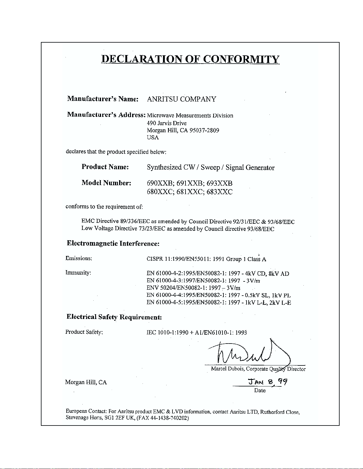
WARRANTY
The Anritsu product(s) listed on the title page is (are) warranted against defects in materials and
workmanship for one year from the date of shipment.
Anritsu's obligation covers repairing or replacing products which prove to be defective during the
warranty period. Buyers shall prepay transportation charges for equipment returned to Anritsu for
warranty repairs. Obligation is limited to the original purchaser.Anritsu is not liable for consequen
tial damages.
LIMITATION OF WARRANTY
The foregoing warranty does not apply to Anritsu connectors that have failed due to normal wear.
Also, the warranty does not apply to defects resulting from improper or inadequate maintenance by
the Buyer, unauthorized modification or misuse, or operation outside of the environmental specifications of the product. No other warranty is expressed or implied, and the remedies provided herein
are the Buyer's sole and exclusive remedies.
TRADEMARK ACKNOWLEDGEMENTS
Adobe Acrobat is a registered trademark of Adobe Systems Incorporated.
NOTICE
Anritsu Company has prepared this manual for use by Anritsu Company personnel and customers
as a guide for the proper installation, operation, and maintenance of Anritsu Company equipment
and computor programs. The drawings, specifications, and information contained herein are the
property of Anritsu Company, and any unauthorized use or disclosure of these drawings, specifica
tions, and information is prohibited; they shall not be reproduced, copied, or used in whole or in part
as the basis for manufacture or sale of the equipment or software programs without the prior writt
ten consent of Anritsu Company.
-
-
-
Page 3
Page 4

Page 5

Table of Contents
Chapter 1 - General Information
1-1 SCOPE OF MANUAL
1-2 INTRODUCTION
1-3 DESCRIPTION
1-4 IDENTIFICATION NUMBER
1-5 ELECTRONIC MANUAL
1-6 RELATED MANUALS
Operation Manual
GPIB Programming Manual
SCPI Programming Manual
1-7 OPTIONS .......................1-6
1-8 LEVEL OF MAINTENANCE.............1-8
Troubleshooting .................1-8
Repair......................1-8
Calibration ...................1-8
Preventive Maintenance .............1-8
1-9 STATIC-SENSITIVE COMPONENT HANDLING
PRECAUTIONS ...................1-8
....................
.................
...................
............
...............
................
................
...........
...........
1-3
1-3
1-3
1-5
1-5
1-5
1-5
1-5
1-5
1-10 PREVENTIVE MAINTENANCE ..........1-10
1-11 STARTUPCONFIGURATIONS
1-12 RECOMMENDED TEST EQUIPMENT
1-13 EXCHANGE ASSEMBLY PROGRAM
1-14 REPLACEABLE SUBASSEMBLIES AND PARTS 1-14
...........
......
.......
1-11
1-12
1-14
Chapter 2 - Functional Description
2-1 INTRODUCTION
2-2 690XXB/691XXB MAJOR SUBSYSTEMS
Digital Control
Front Panel
Frequency Synthesis
Analog Instruction
YIG, SDM, SQM Driver
ALC/Modulation
690XXB/691XXB MM i
...................
......
..................
...................
...............
................
.............
.................
2-3
2-3
2-3
2-4
2-4
2-5
2-5
2-8
Page 6

Table of Contents (Continued)
RF Deck
Power Supply
Inputs/Outputs
Motherboard/Interconnections
2-3 FREQUENCY SYNTHESIS
Phase Lock Loops
Overall Operation
RF Outputs 0.00001 to 65 GHz
Frequency Modulation (691XXB only)
Analog Sweep Mode (691XXB only)
Step Sweep Mode
2-4 ALC AND MODULATION
ALC Loop Operation
Amplitude Modulation (691XXB only) ......2-18
Square Wave Modulation (691XXB only) ....2-18
2-5 RF DECK ASSEMBLIES ..............2-19
RF Deck Configurations ............2-19
YIG-tuned Oscillator ..............2-20
Power Level Control and Modulation ......2-20
RF Signal Filtering ...............2-25
0.01 to 2 GHz Down Converter .........2-26
0.01 to 2.2 GHz Digital Down Converter ....2-27
Switched Doubler Module............2-28
Source Quadrupler Module
Power Level Detection/ALC Loop
Step Attenuators
.....................
..................
.................
..........
.............
................
...............
.........
......
.......
................
..............
..............
...........
........
................
2-8
2-8
2-8
2-9
2-9
2-9
2-10
2-13
2-14
2-14
2-15
2-15
2-15
2-29
2-30
2-31
Chapter 3 - Performance Verification
3-1 INTRODUCTION
3-2 RECOMMENDED TEST EQUIPMENT
3-3 TEST RECORDS
3-4 CONNECTOR AND KEY LABEL NOTATION
3-5 690XXB/691XXB POWER LEVELS
3-6 INTERNAL TIME BASE AGING RATE TEST
Test Setup
Test Procedure
ii 690XXB/691XXB MM
....................
...................
.......
...................
...
.........
...
..................
3-3
3-3
3-3
3-3
3-6
3-7
3-7
3-8
Page 7

Table of Contents (Continued)
3-7 FREQUENCY SYNTHESIS TESTS
Test Setup
Coarse Loop/ YIG Loop Test Procedure
Fine Loop Test Procedure
3-8 SPURIOUS SIGNALS TEST: RF OUTPUT
SIGNALS £2 GHz (£2.2 GHz UNITS
W/OPTION 21A)
Test Setup
0.01 - 2 GHz Test Procedure
0.01 - 2.2 GHz Test Procedure
3-9 HARMONIC TEST: RF OUTPUT SIGNALS
FROM2TO20GHz
Test Setup
2 - 10 GHz Test Procedure
11 - 20 GHz Test Procedure ..........3-18
3-10 SINGLE SIDEBAND PHASE NOISE TEST ....3-20
Test Setup ...................3-20
Test Procedure .................3-21
...................
............
..................
...................
..........
..........
................
...................
...........
........
.....
3-10
3-10
3-10
3-11
3-12
3-12
3-12
3-15
3-16
3-16
3-17
3-11 POWER LEVELACCURACY AND FLATNESS
TESTS........................3-24
Test Setup ...................3-24
Power Level Accuracy Test Procedure ......3-25
Power Level Flatness Test Procedure ......3-26
3-12 AMPLITUDE MODULATION TEST
Test Setup
AM Input Sensitivity Procedure
3-13 FREQUENCY MODULATION TESTS
Test Setup
FM Input Sensitivity Procedure
...................
...................
........
.........
.......
.........
Chapter 4 - Calibration
4-1 INTRODUCTION
4-2 RECOMMENDED TEST EQUIPMENT
4-3 TEST RECORDS
4-4 CALIBRATION FOLLOWING SUBASSEMBLY
REPLACEMENT
...................
.......
...................
...................
3-28
3-28
3-29
3-31
3-31
3-32
4-3
4-3
4-3
4-4
4-5 CONNECTOR AND KEY LABEL NOTATION
690XXB/691XXB MM iii
...
4-4
Page 8

Table of Contents (Continued)
4-6 INITIAL SETUP
Interconnection
PC Setup — Windows 3.1
PC Setup — Windows 95/Windows 98
4-7 PRELIMINARY CALIBRATION
Equipment Setup
Calibration Steps
Alternate Reference Oscillator Calibration
4-8 SWITCHED FILTER SHAPER CALIBRATION
Equipment Setup
Log Amplifier Zero Calibration
Limiter DAC Adjustment
Shaper DAC Adjustment
4-9 RF LEVELCALIBRATION .............4-23
4-10 ALC SLOPE CALIBRATION (691XXB ONLY). . . 4-24
Equipment Setup................4-24
ALC Slope DAC Adjustment ..........4-25
4-11 ALC BANDWIDTH CALIBRATION ........4-28
....................
.................
............
......
..........
................
................
...
................
.........
............
............
..
4-7
4-7
4-8
4-10
4-13
4-13
4-14
4-17
4-19
4-19
4-20
4-20
4-22
Equipment Setup................4-28
Bandwidth Calibration .............4-28
4-12 AM CALIBRATION (691XXB ONLY)........4-30
Equipment Setup
AM Calibration Procedure
4-13 FM CALIBRATION (691XXB ONLY)
Equipment Setup
FM Calibration Procedure
................
...........
........
................
...........
4-30
4-31
4-34
4-34
4-35
Chapter5-Troubleshooting
5-1 INTRODUCTION
5-2 RECOMMENDED TEST EQUIPMENT
5-3 ERROR AND WARNING/STATUS MESSAGES
Self-Test Error Messages
Normal Operation Error and Warning/
Status Messages
5-4 MALFUNCTIONS NOT DISPLAYING AN ERROR
MESSAGE
...................
.......
...
.............
................
.....................
5-3
5-3
5-3
5-3
5-7
5-10
iv 690XXB/691XXB MM
Page 9

Table of Contents (Continued)
5-5 TROUBLESHOOTING TABLES
..........
5-10
Chapter 6 - Removal and Replacement Procedures
6-1 INTRODUCTION
6-2 REMOVING AND REPLACING THE CHASSIS
COVERS
Preliminary
Procedure
6-3 REMOVING AND REPLACING THE FRONT
PANEL ASSEMBLY
Preliminary
Procedure
6-4 REMOVING AND REPLACING THE A3, A5,
ORA6PCB......................6-8
Preliminary ...................6-8
Procedure ....................6-8
6-5 REMOVING AND REPLACING THE A4 PCB . . . 6-8
Preliminary ...................6-8
Procedure ....................6-8
.......................
....................
....................
...................
...................
.................
...................
6-3
6-4
6-4
6-4
6-6
6-6
6-6
6-6 REMOVING AND REPLACING THE A7 PCB. . . 6-10
Preliminary ..................6-10
Procedure ...................6-10
6-7 REMOVING AND REPLACING THE A9, A10,
A11, OR A12 PCB
Preliminary
Procedure
6-8 REMOVING AND REPLACING THE A13
OR A15 PCB
Preliminary
Procedure
6-9 REMOVING AND REPLACING THE A14 PCB
Preliminary
Procedure
6-10 REMOVING AND REPLACING THE A16
OR A17 PCB
Preliminary
Procedure
...................
...................
...................
...................
...................
...................
..................
..................
....................
..
....................
..................
6-10
6-10
6-10
6-11
6-11
6-11
6-11
6-11
6-11
6-13
6-13
6-13
690XXB/691XXB MM v
Page 10

Table of Contents (Continued)
6-11 REMOVING AND REPLACING THE A18
OR A19 PCB
Preliminary
Procedure
6-12 REMOVING AND REPLACING THE REAR
PANEL ASSEMBLY
Preliminary
Procedure
....................
..................
...................
.................
..................
...................
6-13
6-13
6-13
6-14
6-14
6-14
6-13 REMOVING AND REPLACING THE A21 PCB
Preliminary
Procedure
6-14 REMOVING AND REPLACING THE
A21-1/A21-2 PCB
Preliminary ..................6-18
Procedure ...................6-18
6-15 REMOVING AND REPLACING THE FAN
ASSEMBLY .....................6-19
Preliminary ..................6-19
Procedure ...................6-19
..................
...................
..................
..
6-17
6-17
6-17
6-18
Appendix A - Test Records
A-1 INTRODUCTION...................A-1
vi 690XXB/691XXB MM
Page 11

Chapter 1
General Information
Table of Contents
1-1 SCOPE OF MANUAL
1-2 INTRODUCTION
1-3 DESCRIPTION
1-4 IDENTIFICATION NUMBER
1-5 ELECTRONIC MANUAL...............1-5
1-6 RELATED MANUALS ................1-5
Operation Manual ................1-5
GPIB Programming Manual ...........1-5
SCPI Programming Manual ...........1-5
1-7 OPTIONS .......................1-6
1-8 LEVEL OF MAINTENANCE.............1-8
Troubleshooting .................1-8
Repair
Calibration
Preventive Maintenance
1-9 STATIC-SENSITIVE COMPONENT
HANDLING PRECAUTIONS
......................
....................
...................
.................
...................
............
.............
............
1-3
1-3
1-3
1-5
1-8
1-8
1-8
1-8
1-10 PREVENTIVE MAINTENANCE
1-11 STARTUPCONFIGURATIONS
1-12 RECOMMENDED TEST EQUIPMENT
1-13 EXCHANGE ASSEMBLY PROGRAM
1-14 REPLACEABLE SUBASSEMBLIES AND PARTS 1-14
..........
...........
......
.......
1-10
1-11
1-12
1-14
Page 12
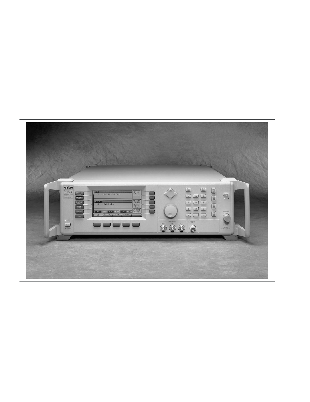
Figure 1-1. Typical Series 690XXB/691XXB Synthesized CW/Signal Generator (Model 69187B Shown)
Page 13

Chapter 1
General Information
1-1 SCOPE OF MANUAL This manual provides service information for all models of the Series
690XXB Synthesized CW Generator and the Series 691XXB Synthe
sized Signal Generator. The service information includes replaceable
parts information, functional circuit descriptions, block diagrams, per
formance verification tests, and procedures for calibration, trouble
shooting, and assembly/subassembly removal and replacement.
(Throughout this manual, the term 690XXB/691XXB is used to refer
to the instrument.) Manual organization is shown in the table of con
tents.
NOTE
Service information for the series 690XXB CW generators
and series 691XXB signal generators is combined into one
manual because identical model numbers of each series contain the same assemblies, subassemblies, and components.
Differences between the series are noted where applicable
throughout the manual.
-
-
-
-
1-2 INTRODUCTION This chapter provides a general description of the Series 690XXB/
691XXB Synthesized CW/Signal Generators, identification numbers,
related manuals, and options. Information is included concerning level
of maintenance, replaceable subassemblies and RF components, ex
change assembly program, and preventive maintenance. Staticsensitive component handling precautions and lists of exchangeable
subassemblies and recommended test equipment are also provided.
1-3 DESCRIPTION The Series 690XXB Synthesized CW Generator and the Series
691XXB Synthesized Signal Generator are microprocessor-based, syn
thesized signal sources with high resolution phase-lock capability.
They generate both discrete CW frequencies and broad (full range)
and narrow band sweeps across the frequency range of 10 MHz to
65 GHz. All functions of the 690XXB/691XXB are fully controllable lo
cally from the front panel or remotely (except for power on/standby)
via the IEEE-488 General Purpose Interface Bus (GPIB).
The Series 690XXB Synthesized CW Generator and the Series
691XXB Synthesized Signal Generator each presently consists of
seven models covering a variety of frequency ranges and power levels.
Table 1-1, on page 1-4, lists models, frequency ranges, and maximum
leveled output.
-
-
-
690XXB/691XXB MM 1-3
Page 14

GENERAL 690XXB/691XXB
INFORMATION MODELS
Table 1-1. Series 690XXB/691XXB Models
69XXXB
Model
69X17B 0.01 – 8.4 GHz +13.0 dBm +11.0 dBm +9.0 dBm
69X37B 2.0 – 20.0 GHz +13.0 dBm +11.0 dBm +3.0 dBm
69X47B 0.01 – 20.0 GHz +13.0 dBm +11.0 dBm +3.0 dBm
69X67B
69X77B
69X87B
69X97B
Frequency
(GHz)
0.01 – 2.0 GHz
2.0 – 20.0 GHz
20.0 – 40.0 GHz
0.01 – 2.0 GHz
2.0 – 20.0 GHz
20.0 – 40.0 GHz
40.0 – 50.0 GHz
0.01 – 2.0 GHz
2.0 – 20.0 GHz
20.0 – 40.0 GHz
40.0 – 50.0 GHz
50.0 – 60.0 GHz
0.01 – 2.0 GHz
2.0 – 20.0 GHz
20.0 – 40.0 GHz
40.0 – 50.0 GHz
50.0 – 65.0 GHz
Output Power
+13.0 dBm
+9.0 dBm
+6.0 dBm
+12.0 dBm
+10.0 dBm
+2.5 dBm
+2.5 dBm
+12.0 dBm
+10.0 dBm
+2.5 dBm
+2.0 dBm
+2.0 dBm
+12.0 dBm
+10.0 dBm
+2.5 dBm
0.0 dBm
–2.0 dBm
With Option 15A (High Power) Installed
Output Power
w/Step Attenuator
+11.0 dBm
+7.0 dBm
+3.0 dBm
+10.0 dBm
+8.5 dBm
0.0 dBm
–1.0 dBm
+10.0 dBm
+8.5 dBm
0.0 dBm
–1.5 dBm
–2.0 dBm
Not Available Not Available
Output Power
w/Electronic
Step Attenuator
Not Available
Not Available
Not Available
69X17B
69X37B 2.0 – 20.0 GHz +17.0 dBm +15.0 dBm +7.0 dBm
69X47B
69X67B
69X77B 0.01 – 50.0 GHz Standard Standard Not Available
69X87B 0.01 – 60.0 GHz Standard Standard Not Available
69X97B 0.01 – 65.0 GHz Standard Not Available Not Available
Note: In models with Option 22 that have a high-end frequency of£20 GHz, rated output power is reduced by 1 dB.
In models with Option 22 that have a high-end frequency of >20 GHz, rated output power is reduced by 2 dB.
0.01 – 2.0 Ghz
2.0 – 8.4 GHz
0.01 – 2.0 GHz
2.0 – 20.0 GHz
0.01 – 2.0 GHz
2.0 – 20.0 GHz
20.0 – 40.0 GHz
+13.0 dBm
+17.0 dBm
+13.0 dBm
+17.0 dBm
+13.0 dBm
+13.0 dBm
+6.0 dBm
+11.0 dBm
+15.0 dBm
+11.0 dBm
+15.0 dBm
+11.0 dBm
+11.0 dBm
+3.0 dBm
+11.0 dBm
+11.0 dBm
+11.0 dBm
+7.0 dBm
Not Available
1-4 690XXB/691XXB MM
Page 15

GENERAL IDENTIFICATION
INFORMATION NUMBER
1-4 IDENTIFICATION NUMBER All Anritsu instruments are assigned a unique six-digit ID number,
such as “875012”. The ID number is imprinted on a decal that is af
fixed to the rear panel of the unit. Special-order instrument configura
tions also have an additional special serial number tag attached to the
rear panel of the unit.
When ordering parts or corresponding with Anritsu Customer Service,
please use the correct serial number with reference to the specific in
strument's model number (i.e., Model 69147B Synthesized Signal Gen
erator, Serial No. 875012).
-
-
1-5 ELECTRONIC MANUAL This manual is available on CD ROM as an Adobe Acrobat Portable
Document Format (*.pdf) file. The file can be viewed using Acrobat
Reader, a free program that is also included on the CD ROM. The file
is "linked” such that the viewer can choose a topic to view from the
displayed "bookmark” list and "jump” to the manual page on which the
topic resides. The text can also be word-searched. Contact Anritsu
Customer Service for price and availablility.
-
-
1-6 RELATED MANUALS This is one of a four manual set that consists of an Operation Manual,
a GPIB Programming Manual, a SCPI Programming Manual, and a
Maintenance Manual.
Operation
Manual
GPIB
Programming
Manual
This manual provides instructions for operation of
the 690XXB/691XXB using the front panel controls.
It also includes general information, performance
specifications, installation instructions, and opera
tion verification procedures. The Anritsu part
number for the Series 690XXB Operation Manual is
10370-10341; the part number for the Series
691XXB Operation Manual is 10370-10344.
This manual provides information for remote opera
tion of the 690XXB/691XXB using Product Specific
commands sent from an external controller via the
IEEE 488 General Purpose Interface Bus (GPIB). It
contains a complete listing and description of all
690XXB/691XXB GPIB Product Specific commands
and several programming examples. The Anritsu
part number for the Series 690XXB GPIB Program
ming Manual is 10370-10342; the part number for
the Series 691XXB GPIB Programming Manual is
10370-10345.
-
-
-
SCPI
Programming
Manual
This manual provides information for remote opera
tion of the 690XXB/691XXB using Standard Com
mands for Programmable Instruments (SCPI)
commands sent from an external controller via the
-
690XXB/691XXB MM 1-5
-
Page 16
GENERAL
INFORMATION OPTIONS
IEEE 488 General Purpose Interface Bus (GPIB). It
contains a complete listing and description of each
command in the 690XXB/691XXB SCPI command
set and examples of command usage. The Anritsu
part number for the Series 690XXB SCPI Program
ming Manual is 10370-10343; the part number for
the Series 691XXB SCPI Programming Manual is
10370-10346.
1-7 OPTIONS The following instrument options are available.
Option 1, Rack Mounting. Rack mount kit containing a set of
q
track slides (90° tilt capability), mounting ears, and front panel
handles for mounting the instrument in a standard 19-inch
equipment rack.
Option 2A, 110 dB Step Attenuator. Adds a 10 dB per step
q
attenuator with a 110 dB range for models having a high-end frequency of £20 GHz. Output power is selected directly in dBm on
the front panel (or via GPIB). Rated output power is reduced.
-
Option 2B, 110 dB Step Attenuator. Adds a 10 dB per step
q
attenuator with a 110 dB range for models having a high-end frequency of £40 GHz. Output power is selected directly in dBm on
the front panel (or via GPIB). Rated output power is reduced.
q
Option 2C, 90 dB Step Attenuator. Adds a 10 dB per step
attenuator with a 90 dB range for models having a high-end frequency of £50 GHz. Output power is selected directly in dBm on
the front panel (or via GPIB). Rated output power is reduced.
q
Option 2D, 90 dB Step Attenuator. Adds a 10 dB per step
attenuator with a 90 dB range for models having a high-end fre
quency of £60 GHz. Output power is selected directly in dBm on
the front panel (or via GPIB). Rated output power is reduced.
q
Option 2E, 120 dB Electronic Step Attenuator. Addsa10dB
per step electonic attenuator with a 120 dB range for models hav
ing a high end frequency of £8.4 Ghz. Output power is selected
directly in dBm on the front panel (or via GPIB). Rated output
power is reduced.
q
Option 2F, 120 dB Electronic Step Attenuator. Addsa10dB
per step electonic attenuator with a 120 dB range for models hav
ing a high end frequency of £20 Ghz. Output power is selected di
rectly in dBm on the front panel (or via GPIB). Rated output
power is reduced.
-
-
-
-
q
Option 9, Rear Panel RF Output. Moves the RF output con
nector to the rear panel.
q
Option 11, 0.1 Hz Frequency Resolution. Provides frequency
resolution of 0.1 Hz.
-
1-6 690XXB/691XXB MM
Page 17
GENERAL
INFORMATION OPTIONS
Option 14, Rack Mounting without Chassis Slides. Modifies
q
rack mounting hardware to install unit in console that has
mounting shelves. Includes mounting ears and front panel han
dles.
-
Option 15A, High Power Output. Adds high-power RF compo
q
nents to the instrument in the 2–20 GHz frequency range. Op
tion 15A is standard in models having a high-end frequency that
is >40 GHz.
Option 16, High-Stability Time Base. Adds an ovenized,
q
10 MHz crystal oscillator with <5 x 10
Options 17A & 17B, No Front Panel. Deletes the front panel
q
–10
/day frequency stability.
for use in remote control applications where a front panel display
or keyboard control are not needed. Option 17A deletes the front
panel from 691XXB models; Option 17B deletes the front panel
from 690XXB models.
Option 18, mmWave Module Bias Output. Provides bias out
q
put for 54000-xWRxx Millimeter Wave Source Modules. BNC
Twinax connector, rear panel.
Option 19, SCPI Programmability. Adds GPIB command
q
mnemonics complying with Standard Commands for Programmable Instruments (SCPI), Version 1993. SCPI programming
complies with IEEE 488.2-1987.
q
Option 21A, Digital Down Converter. Replaces the standard
Analog Down Converter (0.01 to 2.0 GHz) with a Digital Down
Converter (0.01 to 2.2 GHz).
q
Option 22, 0.1 Hz to 10 MHz Audio Frequency. Adds fre
quency coverage below 10 Mhz. In models having a high-end fre
quency of £20 GHz, rated output power is reduced by 1 dB; in
models having a high-end frequency of >20 GHz, rated output
power is reduced by 2 dB.
-
-
-
-
-
690XXB/691XXB MM 1-7
Page 18

GENERAL LEVEL OF
INFORMATION MAINTENANCE
1-8 LEVEL OF MAINTENANCE Maintenance of the 690XXB/691XXB consists of:
Troubleshooting the instrument to a replaceable subassembly or
q
RF component.
Repair by replacing the failed subassembly or RF component.
q
Calibration.
q
Preventive maintenance.
q
Troubleshoot
ing
Repair Most instrument failures are field repairable by
Calibration The 690XXB/691XXB may require calibration after
Preventive
Maintenance
The 690XXB/691XXB firmware includes internal
-
diagnostics that self-test most of the internal assem
blies of the instrument. When the 690XXB/691XXB
fails self-test, one or more error messages are dis
played to aid in troubleshooting the failure to a
replaceable subassembly or RF component. Chapter
5–Troubleshooting lists and describes the self-test
error messages and provides procedures for isolat
ing 690XXB/691XXB failures to a replaceable subas
sembly or RF component.
replacing the failed subassembly or RF component.
Detailed instructions for removing and replacing
failed subassemblies and components are provided
in Chapter 6–Removal and Replacement Procedures.
repair. Refer to Chapter 4–Calibration for a listing
of calibration requirements and calibration proce
dures.
Preventive maintenance on the 690XXB/691XXB
consists of cleaning the fan honeycomb filter, de
scribed in paragraph 1-10.
-
-
-
-
-
-
1-9 STATIC-SENSITIVE
COMPONENT HANDLING
PRECAUTIONS
The 690XXB/691XXB contains components that can be damaged by
static electricity. Figure 1-2 illustrates the precautions that should be
followed when handling static-sensitive subassemblies and compo
nents. If followed, these precautions will minimize the possibilities of
static-shock damage to these items.
NOTE
Use of a grounded wrist strap when removing and/or replac
ing subassemblies or components is strongly recommended.
-
-
1-8 690XXB/691XXB MM
Page 19

GENERAL STATIC-SENSITIVE COMPONENT
INFORMATION HANDLING PRECAUTIONS
1. Do not touch exposed contacts
on any static sensitive compo
nent.
4. Wear a static-discharge wristband when working with static
sensitive components.
2 Do not slide static sensitive
-
component across any surface.
5. Label all static sensitive
devices.
3. Do not handle static sensitive
components in areas where the
floor or work surface covering
is capable of generating a
static charge.
6. Keep component leads shorted
together whenever possible.
7. Handle PCBs only by their
edges. Do not handle by the
edge connectors.
10. ADDITIONAL PRECAUTIONS:
·
Keep workspaces clean and free of any objects capable of holding or storing a static charge.
·
Connect soldering tools to an earth ground.
·
Use only special anti-static suction or wick-type desoldering tools.
Figure 1-2. Static-Sensitive Compontent Handling Precautions
8. Lift & handle solid state de
vices by their bodies – never
by their leads.
-
9. Transport and store PCBs and
other static sensitive devices
in static-shielded containers.
690XXB/691XXB MM 1-9
Page 20
GENERAL PREVENTIVE
INFORMATION MAINTENANCE
1-10 PREVENTIVE
MAINTENANCE
The 690XXB/691XXB must always receive adequate ventilation. A
blocked fan filter can cause the instrument to overheat and shut down.
Check and clean the rear panel fan honeycomb filter periodically.
Clean the fan honeycomb filter more frequently in dusty environ
ments. Clean the filter as follows.
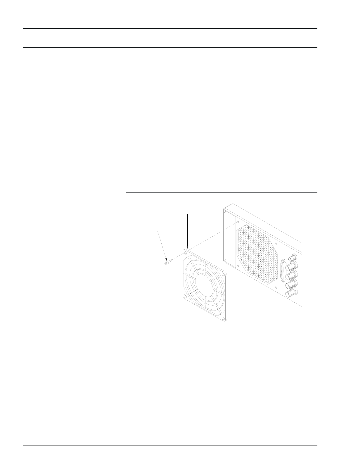
Step 1 Remove the filter guard from the rear panel by pull
ing out on the four panel fasteners holding them in
place (Figure 1-3).
Step 2 Vacuum the honeycomb filter to clean it.
Step 3 Install the filter guard back on the rear panel.
Step 4 Press in on the panel fasteners to secure the filter
guard to the rear panel.
-
-
Figure 1-3. Removing/Replacing the Fan Filter Guard
1-10 690XXB/691XXB MM
Page 21
GENERAL START UP
INFORMATION CONFIGURATION
1-11 STARTUP
CONFIGURATIONS
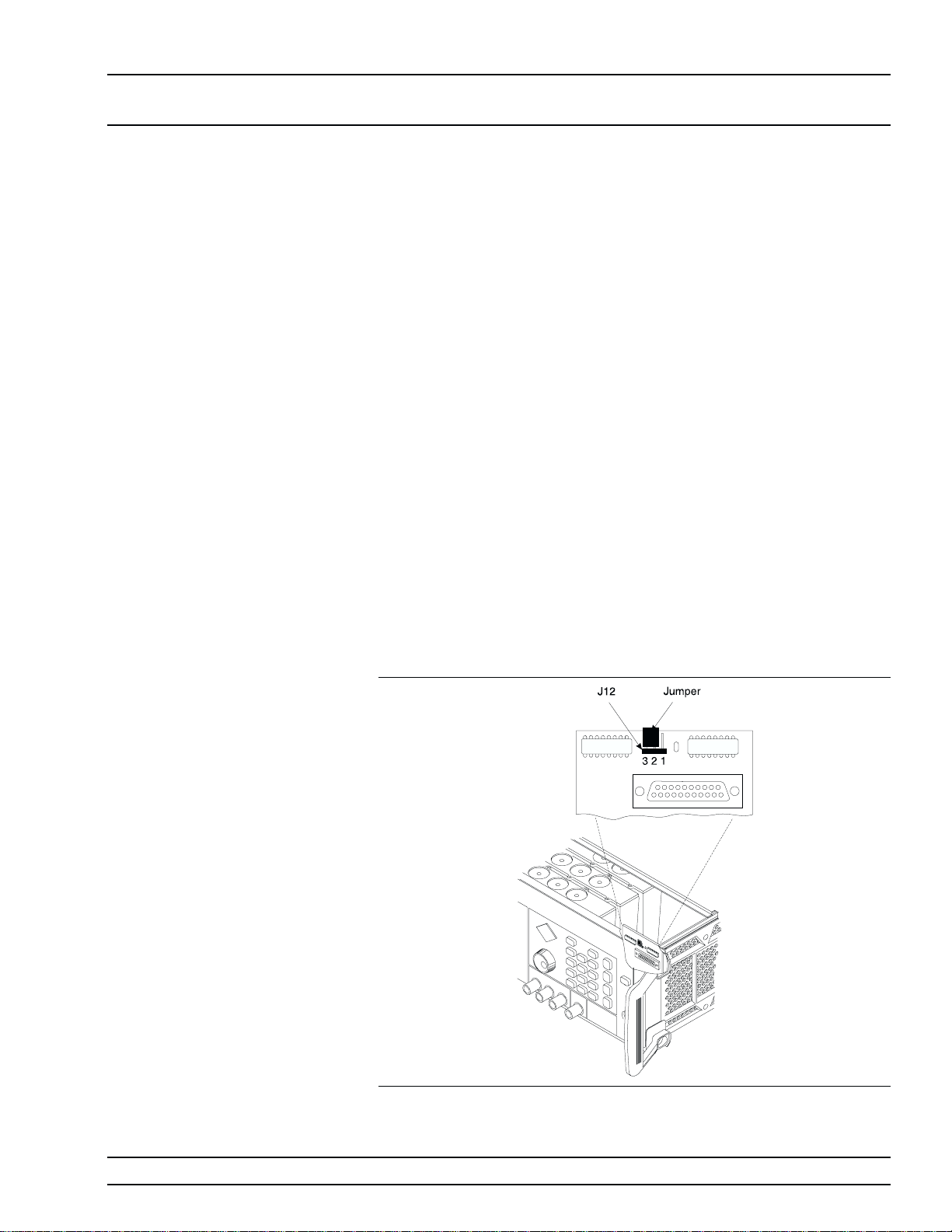
The 690XXB/691XXB comes from the factory with a jumper across
pins 2 and 3 of front panel connector J12 (Figure 1-4). In this configu
ration, connecting the instrument to line power automatically places it
in operate mode (front panel OPERATE LED on).
The startup configuration can be changed so that the 690XXB/691XXB
comes up in standby mode (front panel STANDBY LED on) when it is
connected to line power. Change the startup configuration as follows:
Step 1 Disconnect the instrument from line power.
Step 2 Remove the top cover from the 690XXB/691XXB.
(Refer to Chapter 6 for instructions).
Step 3 Locate front panel connector J12 and remove the
jumper from across pins 2 and 3. It is located on the
A2A1 PCB which plugs into the Front Panel Assem
bly.
Step 4 Install the jumper across pins 1 and 2 of connector
J12.
Step 5 Install the top cover and connect the 690XXB/
691XXB to line power. The instrument should come
up in standby mode.
-
-
Figure 1-4. Startup Configuration of Connector J12
690XXB/691XXB MM 1-11
Page 22
GENERAL RECOMMENDED
INFORMATION TEST EQUIPMENT
1-12 RECOMMENDED TEST
EQUIPMENT
Table 1-2 provides a list of recommended test equipment needed for
the performance verification, calibration, and troubleshooting proce
dures presented in this manual.
Table 1-2. Recommended Test Equipment (1 of 2)
INSTRUMENT
Spectrum Analyzer,
with
External Mixers
and
Diplexer Assy
Phase Noise
Measurement
System
Frequency Counter Frequency Range: 0.01 to 40 GHz
Power Meter,
with
Power
Sensors
Digital Multimeter Resolution: 4-1/2 digits (to 20V)
Frequency Reference Frequency: 10 MHz
Function Generator Output Voltage: 2 volts peak-to-peak
Modulation Analyzer Frequency Input: 10 MHz
Frequency Range: 0.01 to 65 GHz
Resolution Bandwidth: 10 Hz
Frequency Range: 5 MHz to 26.5 GHz Aeroflex/Comstron PN9000
Input Impedance: 50
Resolution: 1Hz
Other: External Time Base Input
Power Range: –30 to +20 dBm
DC Accuracy: 0.002% +2 counts
DC Input Impedance: 10 M
AC Accuracy: 0.07% +100 counts
AC Input Impedance: 1M
Accuracy: 5x10
Functions: 0.4 Hz to 100 kHz sine and
square waveforms
(of the IF of the spectrum analyzer)
AM Depth: 0% to 90%
AM Modulation Rates: DC to 100 kHz
Filters: 20 kHz lowpass, 300 Hz highpass
CRITICAL
SPECIFICATION
W
(1mW to 100mW)
W
(to 20 kHz)
W
-12
parts/day
RECOMMENDED
MANUFACTURER/MODEL USAGE
Tektronix, Model 2794, with
External Mixers:
WM780K (18 to 26.5 GHz)
WM780A (26.5 to 40 GHz)
WM780U (40 to 60 GHz)
WM780E (60 to 90 GHz)
Diplexer Assy: 015-0385-00
with
PN9060-00 Status Module
PN9470-00 Noise Output Module
PN9450-00 Lock Control Module
PN9342-01 Phase Detector Module
PN9530-00 Crystal Oscillator Module
Anritsu Model MF2414A C, P
Anritsu Model ML2437A or ML2438A,
with
Power Sensors:
MA2474A (0.01 to 40 GHz)
MA2475A (0.01 to 50 GHz)
John Fluke, Inc., Model 8840A, with
Option 8840A-09K (True RMS AC)
Absolute Time Corp., Model 300 P
Hewlett-Packard, Model 33120A C, P
Hewlett-Packard, Model 8901A P
C, P,T
P
C, P
C, T
-
(1)
1-12 690XXB/691XXB MM
Page 23
GENERAL RECOMMENDED
INFORMATION TEST EQUIPMENT
Table 1-2. Recommended Test Equipment (2 of 2)
INSTRUMENT
Oscilloscope Bandwidth: DC to 150 MHz
Vertical Sensitivity: 2mV/division
Horizontal Sensitivity: 50 ns/division
Scalar Network
Analyzer, with
RF Detector
Attenuator Frequency Range: DC to 40 GHz
Attenuator Frequency Range: DC to 40 GHz
Attenuator Frequency Range: DC to 60 GHz
Attenuator Frequency Range: DC to 60 GHz
RF Detector Frequency Range: 0.01 to 40 GHz
RF Detector Frequency Range: 0.01 to 50 GHz
Personal Computer PC Configuration: IBM ATor compatible
Serial Interface Assy Provides serial interface between the PC
Special AUX I/O
Cable Assy
Tee Connectors: 50WBNC Any common source C, P
Cables Connectors: 50WBNC Any common source C, P,T
Frequency Range: 0.01 to 60 GHz Anritsu, Model 56100A, with
Max Input Power: >+17 dBm
Attenuation: 10 dB
Max Input Power: >+17 dBm
Attenuation: 20 dB
Max Input Power: >+17 dBm
Attenuation: 10 dB
Max Input Power: >+17 dBm
Attenuation: 20 dB
Output Polarity: Negative
Output Polarity: Negative
Operating System: Windows 3.1, 95, or
98
Accessories: Mouse
and the 690XXB/691XXB.
Provides interface between the 690XXB/
691XXB and the Power Meter
CRITICAL
SPECIFICATION
Tektronix, Inc. Model TAS485 P, T
RF Detector:
560-7K50 (0.01 to 40 GHz)
560-7VA50(0.01 to 50 GHz)
SC5198 (40 to 60 GHz)
Anritsu, Model 41KC-10 C, P
Anritsu, Model 41KC-20 P
Anritsu, Model 41V-10 C, P
Anritsu, Model 41V-20 P
Anritsu, Model 75KC50
(K input/BNC output connectors)
Anritsu, Model 75VA50
(V input/BNC output connectors)
Any common source C
Anritsu P/N: T1678 C
Anritsu P/N: 806-90 P
RECOMMENDED
MANUFACTURER/MODEL USAGE
C, T
T
T
(1)
NOTES: (1) P = Performance Verification Tests (Chapter 3); C = Calibration (Chapter 4); T = Troubleshooting (Chapter 5)
690XXB/691XXB MM 1-13
Page 24

GENERAL EXCHANGE
INFORMATION ASSEMBLY PROGRAM
1-13 EXCHANGE ASSEMBLY
PROGRAM
1-14 REPLACEABLE
SUBASSEMBLIES AND
PARTS
Anritsu maintains an exchange assembly program for selected
690XXB/691XXB subassemblies and RF components. If a malfunction
occurs in one of these subassemblies, the defective unit can be
exchanged. Upon receiving your request, Anritsu will ship the
exchange subassembly or RF component to you, typically within 24
hours. You then have 45 days in which to return the defective item. All
exchange subassemblies or RF components are warranted for 90 days
from the date of shipment, or for the balance of the original equipment
warranty, whichever is longer.
Please have the exact model number and serial number of your unit
available when requesting this service, as the information about your
unit is filed according to the instrument's model and serial number.
For more information about the program, contact your local sales rep
resentative or call your local Anritsu service center. Refer to Table 1-5,
on page 1-18, for a list of current Anritsu service centers.
Table 1-3, on page 1-15, lists those replaceable subassemblies and RF
components of the 690XXB/691XXB that are presently covered by the
Anritsu exchange assembly program. Table 1-4, on page 1-16, lists
common replaceable parts for the 690XXB/691XXB that are not presently on the exchange assembly program.
All parts listed in Tables 1-3 and 1-4 may be ordered from your local
Anritsu service center.
-
1-14 690XXB/691XXB MM
Page 25

GENERAL
INFORMATION PARTS LIST
Table 1-3. Replaceable Subassemblies and RF Components (1 of 2)
SUBASSEMBLY OR PART NAME ANRITSU PART NUMBER
Printed Circuit Board Assemblies
Front Panel Assy 691XXB ND40832
Front Panel Assy 690XXB ND40514
A3 Reference Loop PCB Assy D40603-4
A4 Coarse Loop PCB Assy D40624-3
A5 Fine Loop PCB Assy D40625-3
A6 Square Wave Generator PCB Assy D37406-3
A7 YIG Loop PCB Assy D40627-3
A9 PIN Control PCB Assy D40659-3
A10 ALC PCB Assy (691XXB) D40610-3
A10 ALC PCB Assy (690XXB) D40610-4
A11FM PCB Assy (All 691XXBs except 69117B) D40651-3
A11FM PCB Assy (69117B only) D40651-4
A11FM PCB Assy (All 690XXBs except 690117B) D40651-5
A11FM PCB Assy (69017B only) D40651-6
A12 Analog Instruction PCB Assy (691XXB) D37448-3
A12 Analog Instruction PCB Assy (690XXB) D40612-3
A13 10 MHz DDS PCB Assy D40653-3
A14 YIG, SDM Driver PCB Assy
(£40 GHz models)
A14 YIG, SDM, SQM Driver PCB Assy
(>40 GHz models)
A15 Regulator PCB Assy D40655-3
A16 CPU Interface PCB Assy D37416-3
A17 CPU PCB Assy D37444-3
A18 Power Supply PCB Assy D40638-3
A19 Power Conditioner PCB Assy D40649-3
A21 Line Filter/Rectifier PCB Assy ND49529
A21-1 BNC/AUX I/O Connector PCB Assy
690XXB
A21-2 BNC/AUX I/O Connector PCB Assy
691XXB
10 MHz Crystal Oscillator Assy D37332
40654-3
40654-4
ND49525
ND40526
RF Components
YIG-Tuned Oscillator, 2 to 20 GHz 48514
YIG-Tuned Oscillator, 2 to 8.4 GHz 37266
Down Converter D27330
Digital Down Converter 50722-1
Switched Doubler Module, 20 to 40 GHz D28540
Source Quadrupler Module, 40 to 50 GHz D28185
Source Quadrupler Module, 40 to 60 GHz 60-141
690XXB/691XXB MM 1-15
Page 26

GENERAL
INFORMATION PARTS LIST
Table 1-3. Replaceable Subassemblies and RF Components (2 of 2)
SUBASSEMBLY OR PART NAME ANRITSU PART NUMBER
RF Components (Continued)
Source Quadrupler Module, 40 to 65 GHz 60-142
Coupler, 40 GHz D27115
Coupler, 60 GHz D27350
Forward Coupler, 60 GHz C27184
Switched Filter D45194
Switched Filter (w/Option 15A) D45198
Output Connector Assy “K” ND39077
Output Connector Assy “V” ND40835
Step Attenuator, 110 dB, 20 GHz D27152
Step Attenuator, 110 dB, 40 GHz D25080
Step Attenuator, 90 dB, 50 GHz D27315
Step Attenuator, 90 dB, 60 GHz D28957
Electronic Step Attenuator, 120 dB, 20 GHz 45720
Diplexer, 10 MHz 46504
Diplexer, <20 GHz 29860
Diplexer, >20 GHz 28850
Table 1-4. Common Replaceable Subassemblies and Parts (1 of 2)
SUBASSEMBLY OR PART NAME ANRITSU PART NUMBER
Cap, Protective (for RF Output K-Connector) A20304
Cap, Protective (for RF Output V-Connector) B37220
Cover, Top D37131
Cover, Bottom D37135
Cover, Side D37133
Cover, Side Handle 761-67
Cover, CPU Housing C37063
Cover, Main Card Cage D37064
Cover, Power Supply Housing C37062
EMI Gasket for side covers 790-437
EMI Gasket for side covers 790-390
EMI Gasket for Front Panel Assy 790-223
1-16 690XXB/691XXB MM
Page 27

GENERAL
INFORMATION PARTS LIST
Table 1-4. Common Replaceable Subassemblies and Parts (2 of 2)
SUBASSEMBLY OR PART NAME ANRITSU PART NUMBER
Fan Assembly A40513
Fan Mount 790-425
Fan Membrane (Honey Comb Filter) C37137
Fan Grill 790-426
Fasteners (for Fan Grill) 790-433
Fuse, 5A, 3AG Slow Blow (110Vac) 631-33
Fuse, 2.5A, 3AG Slow Blow (230 Vac) 631-14
Gasket, RFI (“O”rings for MCX connectors) 790-393
Handle, Side Carrying 783-830
Screw, Handle Side Carrying 900-714
Line Module 260-11
Shield Cover D37228
Shield D37229
Standoff 785-922
Tape 850-70
Foot, Rear Bottom Left 2000-548
Foot, Rear Bottom Right 2000-549
Foot, Rear TopLeft 2000-552
Foot, Rear TopRight 2000-553
Screw, Green Head 2000-560
690XXB/691XXB without Front Handles Installed
Foot, Front Bottom Left 2000-546
Foot, Front Bottom Right 2000-547
Foot, Front TopLeft 2000-550
Foot, Front TopRight 2000-551
690XXB/691XXB with Front Handles Installed
Upper Insert B37147
Foot, Bottom Left C37170
Foot, Bottom Right C37171
Handle, Left D37168-2
Handle, Right D37169-2
Tilt Bail 790-435
690XXB/691XXB MM 1-17
Page 28

GENERAL ANRITSU
INFORMATION SERVICE CENTERS
Table 1-5. Anritsu Service Centers
UNITED STATES
ANRITSU COMPANY
490 Jarvis Drive
Morgan Hill, CA 95037-2809
Telephone: (408) 776-8300
1-800-ANRITSU
FAX: 408-776-1744
ANRITSU COMPANY
10 New Maple Ave., Unit 305
Pine Brook, NJ 07058
Telephone: (973) 227-8999
1-800-ANRITSU
FAX: 973-575-0092
ANRITSU COMPANY
1155 E. Collins Blvd
Richardson, TX 75081
Telephone: 1-800-ANRITSU
FAX: 972-671-1877
AUSTRALIA
ANRITSU PTY. LTD.
Unit 3, 170 Foster Road
Mt Waverley, VIC 3149
Australia
Telephone: 03-9558-8177
FAX: 03-9558-8255
BRAZIL
ANRITSU ELECTRONICA LTDA.
Praia de Botafogo, 440, Sala 2401
CEP22250-040, Rio de Janeiro, RJ, Brasil
Telephone: 021-527-6922
FAX: 021-53-71-456
CANADA
ANRITSU INSTRUMENTS LTD.
700 Silver Seven Road, Suite 120
Kanata, Ontario K2V 1C3
Telephone: (613) 591-2003
FAX: (613) 591-1006
CHINA
ANRITSU ELECTRONICS (SHANGHAI) CO. LTD.
2F, Rm B, 52 Section Factory Building
No. 516 Fu Te Rd (N)
Shanghai 200131 P.R. China
Telephone:21-58680226, 58680227, 58680228
FAX: 21-58680588
FRANCE
ANRITSU S.A
9 Avenue du Quebec
Zone de Courtaboeuf
91951 Les Ulis Cedex
Telephone: 016-09-21-550
FAX: 016-44-61-065
GERMANY
ANRITSU GmbH
Grafenberger Allee 54-56
D-40237 Dusseldorf, Germany
Telephone: 0211-968550
FAX: 0211-9685555
INDIA
MEERA AGENCIES PVT. LTD.
23 Community Centre
Zamroodpur, Kailash Colony Extension,
New Delhi, India 110 048
Phone: 011-2-6442700/6442800
FAX : 011-2-644250023
ISRAEL
TECH-CENT, LTD.
4 Raul Valenberg St
Tel-Aviv 69719
Telephone: (03) 64-78-563
FAX: (03) 64-78-334
ITALY
ANRITSU Sp.A
Roma Office
Via E. Vittorini, 129
00144 Roma EUR
Telephone: (06) 50-99-711
FAX: (06) 50-22-4252
KOREA
ANRITSU CORPORATION LTD.
Head Office:
14F, Hyunjuk Building 832-41
Yeoksam-Dong, Kangnam-Ku
Seoul 135-080, South Korea
Telephone: 02-553-6603
FAX: 02-553-6604
Service Center:
8F Hyunjuk Building
832-41, Yeoksam Dong
Kangnam-Gu
Seoul, South Korea 135-080
Telephone: 82-2-553-6603
FAX: 82-2-553-6605
JAPAN
ANRITSU CUSTOMER SERVICE LTD.
1800 Onna Atsugi-shi
Kanagawa-Prf. 243 Japan
Telephone: 0462-96-6688
FAX: 0462-25-8379
SINGAPORE
ANRITSU (SINGAPORE) PTE LTD.
10, Hoe Chiang Road
#07-01/02 Keppel Towers
Singapore 089315
Telephone: 282-2400
FAX: 282-2533
SOUTH AFRICA
ETECSA
12 Surrey Square Office Park
330 Surrey Avenue
Ferndale, Randburt, 2194
South Africa
Telephone: 011-27-11-787-7200
FAX: 011-27-11-787-0446
SWEDEN
ANRITSU AB
Botivid Center
Fittja Backe 13A
145 84 Stockholmn
Telephone: (08) 534-707-00
FAX: (08) 534-707-30
TAIWAN
ANRITSU CO., INC.
7F, No. 316, Section 1
NeiHu Road
Taipei, Taiwan, R.O.C.
Telephone: 886-2-8751-1816
FAX: 886-2-8751-2126
UNITED KINGDOM
ANRITSU LTD.
200 Capability Green
Luton, Bedfordshire
LU1 3LU, England
Telephone: 015-82-433200
FAX: 015-82-731303
1-18 690XXB/691XXB MM
Page 29

Chapter 2
Functional Description
Table of Contents
2-1 INTRODUCTION
2-2 690XXB/691XXB MAJOR SUBSYSTEMS
Digital Control
Front Panel
Frequency Synthesis...............2-4
Analog Instruction................2-5
YIG, SDM, SQM Driver .............2-5
ALC/Modulation .................2-8
RF Deck.....................2-8
Power Supply ..................2-8
Inputs/Outputs .................2-8
Motherboard/Interconnections ..........2-9
2-3 FREQUENCY SYNTHESIS .............2-9
Phase Lock Loops ................2-9
Overall Operation
RF Outputs 0.00001 to 65 GHz
Frequency Modulation (691XXB only)
Analog Sweep Mode (691XXB only)
Step Sweep Mode
...................
......
..................
...................
...............
.........
......
.......
................
2-3
2-3
2-3
2-4
2-10
2-13
2-14
2-14
2-15
2-4 ALC AND MODULATION
ALC Loop Operation
Amplitude Modulation (691XXB only)
Square Wave Modulation (691XXB only)
2-5 RF DECK ASSEMBLIES
RF Deck Configurations
YIG-tuned Oscillator
Power Level Control and Modulation
RF Signal Filtering
0.01 to 2 GHz Down Converter
0.01 to 2.2 GHz Digital Down Converter
..............
..............
...............
..............
......
....
..............
............
......
.........
....
2-15
2-15
2-18
2-18
2-19
2-19
2-20
2-20
2-25
2-26
2-27
Page 30

Table of Contents (Continued)
Switched Doubler Module
Source Quadrupler Module
Power Level Detection/ALC Loop
Step Attenuators
................
............
...........
........
2-28
2-29
2-30
2-31
Page 31

Chapter 2
Functional Description
2-1 INTRODUCTION This chapter provides brief functional descriptions of the major sub
systems that are contained in each model of the Series 690XXB/
691XXB Synthesized CW/Signal Generators. In addition, the opera
tion of the frequency synthesis, automatic level control (ALC), and RF
deck subsystems is described so that the reader may better under
stand the overall operation of the instrument. Block diagrams are in
cluded to supplement the written descriptions.
2-2 690XXB/691XXB MAJOR
SUBSYSTEMS
The 690XXB/691XXB circuitry consists of various distinct subsystems
that are contained on one or more printed circuit board (PCB) assemblies or in microwave components located on the RF deck. The following paragraphs identify the subsystems that make up the instrument
and provide a brief description of each. Figure 2-1 (page 2-6) is an
overall block diagram of a typical 690XXB/691XXB.
NOTE
Although identical model numbers of the series 690XXB CW
generators and series 691XXB signal generators contain the
same major subsystems, there are some functional differences between them. These functional differences result
fromthe series 691XXB having the additional capability of
producing analog frequency sweeps and AM, FM, and
square wave modulation of the RF output signal. Functional
differences between the series are noted in the following de
scriptions where applicable.
-
-
-
-
-
Digital
Control
This circuit subsystem consists of the A17 CPU and
A16 CPU Interface PCBs. The central processor unit
(CPU) is the main controller for the 690XXB/
691XXB. This controller directly or indirectly con
trols all functions of the instrument. The CPU con
tains memory that stores the main operating system
components and instrument firmware, instrument
calibration data, and front panel setups in the
power-off condition. It has a GPIB interface that
allows it to communicate with external devices over
the GPIB and a serial interface to a serial terminal
port on the rear panel. The CPU is directly linked
via a dedicated data and address bus to the A2
Front Panel PCB, the A9 PIN Control PCB, the A10
ALC PCB, the A11 FM PCB, the A12 Analog
Instruction PCB, the A14 YIG, SDM, SQM Driver
-
-
690XXB/691XXB MM 2-3
Page 32

FUNCTIONAL 690XXB/691XXB
DESCRIPTION MAJOR SUBSYSTEMS
PCB, the A16 CPU Interface PCB, and the optional
A13 10 MHz DDS PCB.
The CPU is indirectly linked via the A16 CPU Inter
face PCB to the A3 Reference Loop PCB, the A4
Coarse Loop PCB, the A5 Fine Loop PCB, and the
A6 Square Wave Generator PCB. The A16 PCB
contains circuitry to perform parallel-to-serial and
serial-to-parallel data conversion. It also contains
circuitry for many of the rear panel signals, a 13-bit
resolution DVM, and decoder circuitry for the front
panel rotary data knob optical encoder.
Front Panel This circuit subsystem consists of the the A1 Front
Panel PCB, the A2 Front Panel Control PCB, and
the Liquid Crystal Display (LCD). This subsystem
interfaces the front panel LCD, LEDs, and keys to
the CPU via the dedicated data and address bus.
The front panel rotary data knob is indirectly linked
to the CPU via the A16 CPU Interface PCB.
The A1 Front Panel PCB contains the keyboard
matrix of conductive rubber switches. The A2 Front
Panel Control PCB has circuits to control the LCD
dot-matrix display, turn the front panel LEDs on
and off, and convert keyboard switch matrix signals
to parallel keycode. It also contains the standby/
operate line switch logic circuit and the optical encoder for the rotary data knob.
-
Frequency
Synthesis
The frequency synthesis subsystem consists of the
A3 Reference Loop PCB, the A4 Coarse Loop PCB,
the A5 Fine Loop PCB, the A7 YIG Loop PCB, and
the A11 FM PCB. It provides the reference frequen
cies and phase lock circuits for precise control of the
YIG-tuned oscillator frequencies, as follows:
q
The A3 Reference Loop PCB supplies the sta
ble 10 MHz, 100 MHz, and 500 MHz reference
frequency signals for the rest of the frequency
synthesis system.
q
The A4 Coarse Loop PCB generates coarse
tuning frequencies of 202.5 to 990 MHz for use
by the YIG Loop.
q
The A5 Fine Loop PCB provides fine tuning
frequencies of 30 to 40 MHz for use by the YIG
Loop.
-
2-4 690XXB/691XXB MM
-
Page 33

FUNCTIONAL 690XXB/691XXB
DESCRIPTION MAJOR SUBSYSTEMS
Analog
Instruction
The A7 YIG Loop PCB performs phase detec
q
tion of the YIG-tuned oscillator's output fre
quency and provides a YIG loop error voltage
to the A11 PCB.
The A11 FM PCB conditions the YIG loop error
q
voltage, producing a correction signal that is
used to fine tune and phase lock the YIG-tuned
oscillator. In the 691XXB, the A11 PCB also
contains circuitry for frequency modulation of
the YIG-tuned oscillator RF output.
The CPU sends control data to the A3 Reference
Loop PCB, the A4 Coarse Loop PCB, and the A5
Fine Loop PCB via the A16 PCB as serial data
words. The CPU controls the A11 FM PCB via the
dedicated data and address bus. Refer to paragraph
2-3 for a functional overview of the frequency syn
thesis subsystem.
The A12 Analog Instruction PCB provides the frequency tuning voltages to the A14 YIG, SDM, SQM
Driver PCB. In addition, it provides a 0V to +10V
ramp signal to the rear panel HORIZ OUT connector,
a V/GHz signal to the rear panel AUX I/O connector,
and a SLOPE signal to the A10 ALC PCB for slopevs-frequency correction of the RF output power. The
A17 CPU controls the A12 Analog Instruction PCB
via the dedicated data and address bus.
-
-
-
YIG, SDM,
SQM Driver
The A14 YIG, SDM, SQM Driver PCB supplies the
tuning current and bias voltages for the YIG-tuned
oscillator. It also provides bias voltages for the
Down Converter assembly and the Switched Filter
assembly. For models with a frequency range
greater than 20 GHz, the A14 PCB supplies bias
voltages for the Switched Doubler Module (SDM)
and the Source Quadrupler Module (SQM). In addi
tion, it provides modulator drive signals for the
SQM.
The A12 Analog Instruction PCB provides frequency
tuning voltages for the main tuning coil driver of the
YIG-tuned oscillator. Thw A17 CPU controls the
A14 YIG, SDM, SQM Driver PCB via the dedicated
data and address bus.
690XXB/691XXB MM 2-5
-
Page 34
FUNCTIONAL 690XXB/691XXB
DESCRIPTION MAJOR SUBSYSTEMS
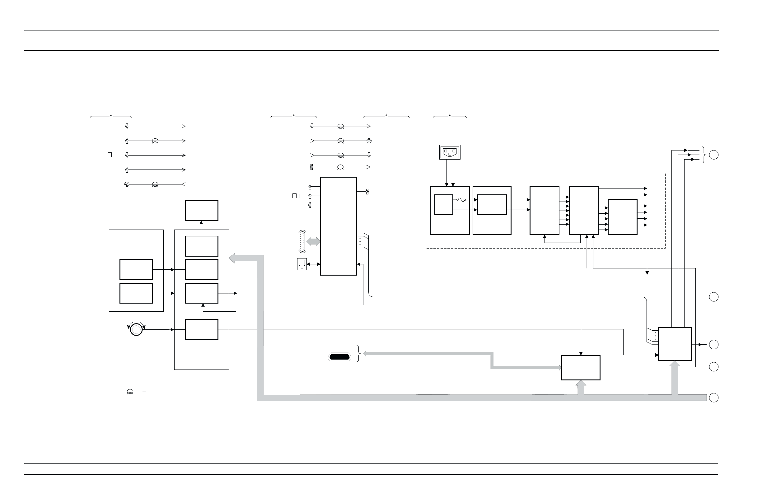
C o n n e c t o r s
A M I N
*
F M I N
*
*
E X T A L C I N
R F O U T P U T
I N
A 1
F r o n t
P a n e l
K e y b o a r d
M a t r i x
L i n e
S w i t c h
R o t a r y
D a t a
K n o b
C o a x i a l C a b l e s
F r o n t P a n e l
T o A 1 0 A L C P C B
( V i a A 2 0 M o t h e r b o a r d )
T o A 1 1 F M P C B
T o A 9 P I N C o n t r o l P C B
( V i a A 2 0 M o t h e r b o a r d )
T o A 1 0 A L C P C B
( V i a A 2 0 M o t h e r b o a r d )
F r o m R F D e c k
L C D
L C D
C o n t r o l
K e y b o a r d
E n c o d e r
L i n e
S w i t c h
L o g i c
O p t i c a l
E n c o d e r
A 2
F r o n t P a n e l
C o n t r o l
+ 2 4 V
( T o A 1 8
P C B )
+ 2 4 V
( F r o m
A 1 5 P C B )
I n p u t s
1 0 M H z R E F I N
F r o m R F D e c k
( O p t i o n 9 )
F r o m A 3
R e f e r e n c e L o o p
F M I N
*
A M I N
*
I N
*
E X T A L C I N
A U X
I / O
S E R I A L
I / O
P h a s e A / P h a s e B D a t a
A 2 1 - 1 / A 2 1 - 2
B N C / A U X
I / O C o n n e c t o r
P C B
I E E E - 4 8 8
R e a r P a n e l
O u t p u t s
T o A 3
R e f e r e n c e L o o p
R F O U T P U T
1 0 M H Z R E F O U T
T o A 1 1 F M P C B
H O R I Z O U T
P o w e r I n p u t
L i n e
F i l t e r
P / O R e a r
C a s t i n g A s s y
G P I B B u s
1 1 0 / 2 2 0 V A C
F u s e
R e a r P a n e l S i g n a l s
B r i d g e
R e c t i f i e r /
D o u b l e r
P / 0 A 2 1
R e a r
P a n e l P C B
P o w e r S u p p l y
+ 1 6 5 V
- 1 6 5 V
S e r i a l I / O
A 1 9
L i n e
C o n d i t i o n e r
A 1 8
P o w e r
S u p p l y
C o n t r o l 4 0 0 k H z
+ 2 4 V
( F r o m A 2 P C B )
A 1 7
C P U
A 1 5
R e g u l a t o r
+ 2 4 V
( T o A 2 P C B )
D i g i t a l
C o n t r o l
D a t a a n d A d d r e s s B u s
+ 5 V
+ 9 V
+ 1 5 V
- 1 5 V
+ 2 4 V
- 2 8 V
A 1 6
C P U
I n t e r f a c e
( C o n t i n u e d o n S h e e t 2 )
A
E
B
C
D
Figure 2-1. Block Diagram of a Typical 690XXB/691XXB
Synthesized CW/Signal Generator (Sheet 1 of 2)
2-6 690XXB/691XXB MM
Page 35

FUNCTIONAL 690XXB/691XXB
(
)
DESCRIPTION MAJOR SUBSYSTEMS
S e r i a l D a t a
S e r i a l D a t a
S e r i a l D a t a
1 0 M H z R E F I N
R e a r P a n e l B N C
A
1 0 M H z
H I - S T A B
X T A L O S C
( O p t i o n )
A 3
R e f e r e n c e
L o o p
1 0 M H z R E F O U T
R e a l P a n e l B N C
1 0 M H z
1 0 0 M H z
5 0 0 M H z
( T o D o w n
C o n v e r t e r )
F r e q u e n c y
S y n t h e s i s
Y I G L o o p E r r o r
A 4
C o a r s e
L o o p
2 0 2 . 5 - 9 9 0 M H z
A 7
Y I G
L o o p
S a m p l e d
2 - 2 0 G H z
R F
1 0 M H z
3 0 - 4 0 M H z
F i n e
L o o p
A 5
1 0 M H z ( T o A 6 )
2 6 . 8 4 3 5 4 5 6 M H z
( T o A 1 3 - O p t i o n 2 2 )
A 1 1
F M
W i d e
F M
A 1 4
Y I G , S D M
A L C
( F r o m A 1 0 )
E
1 0 M H z
( F r o m A 5 )
B
C
D
S e r i a l D a t a
4 0 0 k H z
C o n t i n u e d F r o m S h e e t 1
D r i v e r
F r e q
F r e q
B a n d
T u n i n g
S e l e c t
A 1 2
A n a l o g
I n s t r u c t i o n
R e a r P a n e l S i g n a l s
A 6
S q u a r e
W a v e
G e n e r a t o r
F r o n t P a n e l F M I N
R e a r P a n e l F M I N
F M
M a i n
B i a s
2 - 2 0 G H z
O s c i l l a t o r
B i a s ( t o S D M )
A n a l o g
I n s t r u c t i o n
D a t a A n d A d d r e s s B u s
Y I G
S q u a r e W a v e
A L C / A M / S q u a r e W a v e
M o d u l a t i o n
F r o n t P a n e l E X T A L C I N
M o d u l a t o r
C o n t r o l
S w i t c h e d F i l t e r
8 . 5 G H z L P F
6 . 5 1 - 8 . 5 G H z
5 0 0 M H z
( F r o m A 3 )
R e a r P a n e l
F r o n t P a n e l
R e a r P a n e l A M I N
F r o n t P a n e l A M I N
3 . 3 G H z L P F
5 . 5 G H z L P F
8 . 4 G H z L P F
1 3 . 5 G H z L P F
D o w n C o n v e r t e r
0 . 0 1 - 2 G H z R F
R e a r P a n e l E X T A L C I N
D e t e c t e d
2 0 G H z L P F
S w i t c h C o n t r o l
0 . 0 1 - 2 G H z
0 . 0 1 - 2 0 G H z
A L C
( T o A 1 4 )
R F D e c k
S w i t c h e d D o u b l e r M o d u l e
2 0 - 2 5 G H z
x 2
B i a s
( F r o m A 1 4 )
A 9
P I N
C o n t r o l
S a m p l e /
A L C
H o l d
A 1 0
A L C
2 5 - 3 2 G H z
3 2 - 4 0 G H z
S w i t c h
C o n t r o l
D e t e c t e d
2 - 4 0 G H z R F
0 . 0 1 -
4 0 G H z
0 . 0 1 - 1 0 M H z
( T o R F D e c k
v i a D i p l e x e r s )
A 1 3
1 0 M H z
D D S
( O p t i o n 2 2 )
D i r e c t i o n a l
C o u p l e r
6 9 1 X X B M o d e l s O n l y
2 6 . 8 4 3 5 4 5 6 M H z
( F r o m A 5 )
A t t e n u a t o r
S t e p
A t t e n u a t o r
C o n t r o l
1 1 0 d B
S t e p
( O p t i o n )
R F O u t p u t
0 . 0 1 - 4 0 G H z
Figure 2-1. Block Diagram of a Typical 690XXB/691XXB
Synthesized CW/Signal Generator (Sheet 2 of 2)
690XXB/691XXB MM 2-7
Page 36

FUNCTIONAL 690XXB/691XXB
DESCRIPTION MAJOR SUBSYSTEMS
ALC/
Modulation
RF Deck This subsystem contains those elements related to
This circuit subsystem consists of the A6 Square
Wave Generator PCB, the A9 PIN Control PCB, the
A10 ALC PCB, and part of the A14 YIG, SDM, SQM
Driver PCB. It provides the following:
Level control of the RF output power.
q
In the 691XXB, AM modulation and square
q
wave modulation.
Current drive signals to the PIN switches
q
located in the Switched Filter assembly and
Switched Doubler Module (SDM).
Drive signals for the Step Attenuator (Option
q
2) and the Diplexers (used with Option 22).
The A17 CPU controls the A9 Pin Control PCB, the
A10 ALC PCB, and the A14 YIG, SDM, SQM Driver
PCB via the dedicated data and address bus. It
sends control data to the A6 Square Wave Generator
PCB via the A16 PCB as serial data words. Refer to
paragraph 2-4 for a functional overview of the ALC
and modulation subsystem.
the generation, modulation, and control of the
sweep- and CW-frequency RF signals. These elements include; the YIG-tuned oscillator, the 0.01 to
2 GHz Down Converter assembly, the optional 0.01
to 2.2 GHz Digital Down Converter assembly, the
Switched Filter assembly, the Switched Doubler
Module (SDM), the Source Quadrupler Module
(SQM), the Diplexer, the Directional Coupler/Level
Detector, and the optional Step Attenuator. Refer to
paragraph 2-5 for a functional overview of the RF
deck subsystem.
Power Supply The power supply subsystem consists of the A15
Regulator PCB, the A18 Power Supply PCB, the
A19 Line Conditioner PCB, and part of the A21
Rear Panel PCB and Rear Casting Assembly. It
supplies all the regulated DC voltages used by the
690XXB/691XXB circuits. The voltages are routed
-
Inputs/
Outputs
throughout the instrument via the A20 Mother
board PCB.
The A21-1/A21-2 BNC/AUX I/O Connector PCB and
the A16 CPU Interface PCB contain the interface
circuits for the majority of the rear panel input and
output connectors, including the AUX I/O connector.
2-8 690XXB/691XXB MM
Page 37

FUNCTIONAL FREQUENCY
DESCRIPTION SYNTHESIS
The front panel external ALC input goes via the A20
Motherboard PCB to the A10 ALC PCB; the rear
panel external ALC input goes by way of the A21-1/
A21-2 PCB and the A20 PCB to the A10 PCB. The
rear panel connectors, 10 MHz REF OUT and
10 MHz REF IN, are coupled directly to the A3 Refer
ence Loop PCB via coaxial cables. The rear panel
IEEE-488 GPIB and SERIAL I/O connectors are
connected to the A17 CPU PCB by way of the Moth
erboard PCB.
In 691XXB models, the front panel AM and Square
Wave inputs go by way of the Motherboard PCB to
the internal PCBs—the AM input to the A10 ALC
PCB and the Square Wave input to the A9 PIN Con
trol PCB. The rear panel AM and Square Wave
inputs route via the A21-2 PCB and the Mother
board PCB to their respective internal PCBs. The
front panel and rear panel FM inputs are coupled
directly via coaxial cable to the A11 FM PCB.
-
-
-
-
Motherboard/
Interconnections
The A20 Motherboard PCB and associated cables
provide the interconnections for the flow of data,
signals, and DC voltages between all internal components and assemblies throughout the 690XXB/
691XXB.
2-3 FREQUENCY SYNTHESIS The frequency synthesis subsystem provides phase-lock control of the
690XXB/691XXB output frequency. It consists of four phase-lock loops,
the Reference Loop, the Coarse Loop, the Fine Loop, and the YIG
Loop. The four phase-lock loops, operating together, produce an accu
rately synthesized, low-noise RF output signal. Figure 2-2 (page 2-11)
is an overall block diagram of the frequency synthesis subsystem. The
following paragraphs describe phase-lock loops and the overall opera
tion of the frequency synthesis subsystem.
Phase Lock
Loops
The purpose of a phase-lock loop is to control the
frequency of a variable oscillator in order to give it
the same accuracy and stability as a fixed reference
oscillator. It works by comparing two frequency in
puts, one fixed and one variable, and supplying a
correction signal to the variable oscillator to reduce
the difference between the two inputs. For example,
suppose we have a 10 MHz reference oscillator with
a stability of1x10
that stability to a voltage controlled oscillator
(VCO). The 10 MHz reference signal is applied to
the reference input of a phase-lock loop circuit. The
signal from the VCO is applied to the variable input.
-7
/day, and we wish to transfer
-
-
-
690XXB/691XXB MM 2-9
Page 38

FUNCTIONAL FREQUENCY
DESCRIPTION SYNTHESIS
A phase detector in the phase-lock loop circuit com
pares the two inputs and determines whether the
variable input waveform is leading or lagging the
reference. The phase detector generates a correction
signal that (depending on polarity) causes the VCO
frequency to increase or decrease to reduce any
phase difference. When the two inputs match, the
loop is said to be locked. The variable input from the
VCO then equals the reference input in phase, fre
quency, accuracy, and stability.
In practical applications a frequency divider is
placed between the output of the variable oscillator
and the variable input to the phase-lock loop. The
circuit can then be used to control a frequency that
is an exact multiple of the reference frequency. In
this way, the variable oscillator acquires the stabil
ity of the reference without equaling its frequency.
In the A3 Reference Loop, the 100 MHz ovencontrolled crystal oscillator (OCXO) can be controlled by the phase-lock loop using a 10 MHz reference. This is because a divide-by-ten circuit is
between the OCXO's output and the variable input
to the phase-lock loop. Both inputs to the phase detector will be 10 MHz when the loop is locked.
-
-
-
Overall
Operation
If a programmable frequency divider is used, a
number of frequencies can be phase-locked to the
same reference. The limitation is that all must be
exact multiples of the reference. The A4 Coarse
Loop and A5 Fine Loop both use programmable fre
quency dividers.
The YIG-tuned oscillator generates a high-power RF
output signal that has low broadband noise and low
spurious content. The frequency of the YIG-tuned
oscillator is controlled by means of (1) its main tun
ing coil and (2) its FM (fine tuning) coil. Main tun
ing coil current from the YIG Driver PCB coarsely
tunes the YIG-tuned oscillator to within a few
megahertz of the final output frequency. The YIG
phase-lock loop is then used to fine tune the YIGtuned oscillator to the exact output frequency and to
reduce FM noise close to the carrier.
-
-
-
2-10 690XXB/691XXB MM
Page 39

FUNCTIONAL FREQUENCY
DESCRIPTION SYNTHESIS
1 0 M H z R E F I n
1 0 M H z
H i - S t a b i l i t y
X T A L O s c i l l a t o r
( O p t i o n a l )
A 3 R e f e r e n c e L o o p
P h a s e /
F r e q u e n c y
D e t e c t o r
1 0 0 M H z
R e f e r e n c e
O s c i l l a t o r
P h a s e
E r r o r
1 0 M H z
1 0 0 M H z
÷ 1 0
P o w e r
S p l i t t e r
F M S w e e p
*
( F r o m A 1 2 P C B )
F M I n
*
( F r o n t P a n e l o r
R e a r P a n e l )
F M
1 0 M H z
1 0 0 M H z
D i v i d e r
C o n t r o l
F M
C o i l
D r i v e r
R F
S p l i t t e r
÷ 1 0
B L o o p
F r e q u e n c y
S y n t h e s i z e r
C L o o p
F r e q u e n c y
S y n t h e s i z e r
A 1 1 F M
x 9
P h a s e
E r r o r
P h a s e
E r r o r
9 0 0 M H z
A 4 C o a r s e L o o p
8 0 9 - 9 9 1 M H z
V C O
5 0 0 - 1 0 0 0 M H z
V C O
1 0 M H z
2 0 . 9 -
9 0 M H z
S a m p l e r
÷ 4
÷ 2
S a m p l e r
2 0 2 . 5 -
9 9 0 M H z
1 0 0 k H z
P h a s e E r r o r
( L o o p O s c . # 3 )
P h a s e /
F r e q u e n c y
D e t e c t o r
2 6 . 8 4 M H z
V C X O
÷ 1 0 0
1 0 M H z
1 0 0 k H z
D i g i t a l
S y n t h e s i z e r
2 . 5 - 5 M H z
F r e q u e n c y
S y n t h e s i z e r
P h a s e /
F r e q u e n c y
D e t e c t o r
P h a s e
E r r o r
2 . 5 - 5 M H z
P h a s e
E r r o r
A 5 F i n e L o o p
1 1 9 0 - 1 5 9 0 M H z
V C O
( L o o p O s c . # 1 )
F i n e
L o o p
O s c i l l a t o r # 2
÷ 4
2 9 7 . 5 - 3 9 7 . 5 M H z
÷ 1 0
3 0 0 -
4 0 0 M H z
3 0 - 4 0 M H z
A 7 Y I G L o o p
1 . 9 6 2 5 t o 2 0 . 0 4 G H z
2 0 2 . 5 - 9 9 0 M H z
F M
F M
L P F
S w e e p
Y I G L o o p E r r o r
P h a s e /
F r e q u e n c y
D e t e c t o r
S R D
÷ 1 2 8
÷ 1 2 8
H a r m o n i c s
S a m p l e r
3 0 - 4 0 M H z
3 0 - 4 0 M H z I F
3 0 - 4 0 M H z
S a m p l e d 2 - 2 0 G H z R F
P / O S w i t c h e d F i l t e r
T u n e
( F r o m A 1 2 P C B )
+ 1 8 V G
A 1 4 Y I G , S D M D r i v e r
B i a s
R e g u l a t o r s
M a i n
C o i l
D r i v e r s
M a i n
B i a s
Y I G - T u n e d
O s c i l l a t o r
F M
2 - 2 0 G H z
M o d u l a t o r
C o n t o l
P u l s e
R F O u t
*
6 9 1 X X B M o d e l s O n l y
Figure 2-2. Block Diagram of the Frequency
Synthesis Subsystem
690XXB/691XXB MM 2-11
Page 40

FUNCTIONAL FREQUENCY
DESCRIPTION SYNTHESIS
One input to the YIG Loop is the 202.5 to 990 MHz
signal from the Coarse Loop. This signal is ampli
fied to drive the step-recovery diode. The steprecovery diode produces harmonics of the coarse
loop signal (³1.9625 to 20.04 GHz). These harmonics
are used by the sampler.
-
Table 2-1. RF Output and Loop Frequencies
RF OUTPUT/LOOP FREQUENCIES
(in MHz)
RF OUT COARSE LOOP FINE LOOP
2000 218.055 37.5
3000 217.143 40.0
4000 212.631 40.0
5000 402.000 40.0
6000 464.615 40.0
7000 469.333 40.0
8000 472.941 40.0
9000 821.818 40.0
10000 836.667 40.0
11000 849.231 40.0
12000 926.154 40.0
The other input to the sampler is the RF output sig
nal from the YIG-tuned oscillator. Mixing this RF
output signal sample with the adjacent coarse-loop
harmonic produces a low frequency difference signal
that is the YIG IF signal (30 to 40 MHz).
The 690XXB/691XXB CPU programs the coarse-loop
oscillator's output frequency so that one of its har
monics will be within 30 to 40 MHz of the desired
YIG-tuned oscillator's output frequency. The YIG
Loop phase detector compares the YIG IF signal to
the 30 to 40 MHz reference signal from the Fine
Loop. If there is a difference, the YIG phase detector
fine tunes the YIG-tuned oscillator (via the FM
circuitry and the FM coil drivers) to eliminate any
frequency difference between the two signals.
Phase locking the instrument's output frequency
over a broad frequency range is accomplished by
programming the coarse-loop oscillator's output to
various frequencies that have harmonics close to the
desired operating frequencies. Exact frequency tun
ing for each desired operating frequency is accom
plished by programming the fine-loop oscillator. (In
each case, the YIG-tuned oscillator is first tuned via
the main tuning coil to the approximate desired
operating frequency.) Table 2-1 shows the coarseloop and fine-loop frequencies for some specific RF
output frequencies.
The coarse-loop oscillator has a programming (tun
ing) range of 202.5 to 990 MHz. This provides har
-
monics from ³1.9625 GHz to 20.04 GHz. This allows
any YIG-tuned oscillator output frequency to be
down converted to a YIG IF signal of 30 to 40 MHz.
-
-
The YIG Loop is fine tuned by varying the 30 to
40MHz reference signal applied to the YIG loop
phase detector. By programming the fine-loop oscil
lator, this signal can be adjusted in 1 kHz incre
ments over the 30 to 40 GHz range. The resolution
of the fine-loop oscillator (hence the resolution of the
RF output signal) is 1 kHz, which is much finer
2-12 690XXB/691XXB MM
-
Page 41

FUNCTIONAL FREQUENCY
DESCRIPTION SYNTHESIS
RF Outputs
0.00001 to
65 GHz
than is available from the coarse loop alone. For ap
plications requiring a resolution finer than 1 kHz,
an optional tuning resolution of 0.1 Hz is available.
The Coarse Loop and Fine Loop outputs are derived
from high-stability 10 MHz and 100 MHz signals
generated by the Reference Loop. For applications
requiring even greater stability, the 100 MHz refer
ence oscillator can be phase locked to an optional
10 MHz reference (internal or external).
Refer to the block diagram of the RF Deck shown in
Figure 2-1 (page 2-7) for the following description.
The 690XXB/691XXB uses one YIG-tuned oscillator.
All other frequencies output by the instrument, ex
cept for 0.01 to 10 MHz, are derived from the funda
mental frequencies generated by this YIG-tuned
oscillator.
0.01 to 2 GHz
RF output frequencies of 0.01 to 2 GHz are developed by down converting the fundamental frequencies of 6.51 to 8.5 GHz. This is achieved using a
6.5 GHz local oscillator signal that is phase locked
to the 500 MHz output of the Reference Loop. Precise control of the 0.01 to 2 GHz frequencies to
1 kHz (0.1 Hz with Option 11) resolution is accomplished by phase-lock control of the 6.51 to 8.5 GHz
fundamental frequencies prior to down conversion.
-
-
-
-
20 to 40 GHz
RF output frequencies of 20 to 40 GHz are produced
by doubling the 10 to 20 GHz fundamental frequen
cies. Phase-lock control of the 10 to 20 GHz funda
mental frequencies, accomplished prior to doubling,
ensures precise control of the 20 to 40 GHz frequen
cies to 1 kHz (0.1 Hz with Option 11) resolution.
40 to 65 GHz
RF output frequencies of 40 to 65 GHz are devel
oped by quadrupling of the 10 to 16.25 GHz funda
mental frequencies (refer to Figure 2-7, page 2-24).
Precise control of the 40 to 65 GHz to 1 kHz (0.1 Hz
with Option 11) resolution is accomplished by
phase-lock control of the 10 to 16.25 GHz fundamen
tal frequencies prior to quadrupling.
0.01 to 2.2 GHz (Option 21A)
RF output frequencies of 0.01 to 2.2 GHz are devel
oped by down converting the fundamental frequen
-
-
-
-
-
690XXB/691XXB MM 2-13
-
-
-
Page 42

FUNCTIONAL FREQUENCY
DESCRIPTION SYNTHESIS
cies of 2 to 4.4 GHz (refer to Figure 2-8, page 2-27).
This is accomplished by successive binary division of
the 2 to 4.4 GHz RF signal. Phase-lock control of the
2 to 4.4 GHz fundamental frequencies, achieved
prior to down converting, ensures precise control of
the 0.01 to 2.2 GHz frequencies to 1 kHz (0.1 Hz
with Option 11) resolution.
0.01 to 10 MHz (Option 22)
RF output frequencies of 0.01 to 10 MHz are pro
duced by instruments with Option 22. The 0.01 to
10 MHz signal is generated by the Direct Digital
Synthesizer on the A13 10 MHz DDS PCB, installed
by Option 22. Precise control of the 0.01 to 10 MHz
frequencies to 0.1 Hz resolution is achieved by
phase-lock control of the 26.8435456 MHz signal
from the A5 Fine Loop PCB that is doubled to pro
duce the clock frequency for the DDS.
-
-
NOTE
For 691XXBs with Option 21A at
frequenciesof£2.2 GHz,broad-band
analog frequency sweeps are
>25 MHz wide; narrow-band fre
quency sweeps are £25 MHz
Frequency
Modulation
(691XXB only)
Analog Sweep
Mode
(691XXB only)
-
Frequency modulation (FM) of the YIG-tuned oscillator RF output by external signals is performed by
summing the external modulating signal into the
FM control path of the YIG loop. Refer to Figures
2-1 and 2-2. The external modulating signal comes
from the front panel or rear panel FM IN input. Circuits on the A11 FM PCB adjust the modulating signal for the proper amount of FM for the sensitivity
selected, then sum it into the YIG loop FM control
path. There, it frequency modulates the RF output
signal by controlling the YIG-tuned oscillator's FM
(fine tuning) coil current.
Broad-band analog frequency sweeps (>100 MHz
wide) of the YIG-tuned oscillator RF output are ac
complished by applying appropriate analog sweep
ramp signals, generated by the A12 Analog Instruc
tion PCB, to the YIG-tuned oscillator's main tuning
coil (via the A14 YIG, SDM, SQM Driver PCB). In
this mode, the start, stop, and bandswitching fre
quencies are phase-lock-corrected during the sweep.
Narrow-band analog frequency sweeps (£100 MHz
wide) of the YIG-tuned oscillator RF output are ac
complished by summing appropriate analog sweep
ramp signals, generated by the A12 Analog Instruc
tion PCB, into the YIG-tuned oscillator's FM tuning
coil control path. The YIG-tuned oscillator's RF out
put is then swept about a center frequency. The cen
ter frequency is set by applying a tuning signal (also
from the A12 PCB) to the YIG-tuned oscillator's
-
-
-
-
-
-
-
2-14 690XXB/691XXB MM
Page 43

FUNCTIONAL ALC AND
DESCRIPTION MODULATION
main tuning coil (via the A14 YIG, SDM, SQM
Driver PCB). In this mode, YIG loop phase locking
is disabled except during center frequency correc
tion, which occurs during sweep retrace.
-
Step Sweep
Mode
Step (digital) frequency sweeps of the YIG-tuned
oscillator RF output consist of a series of discrete,
synthesized steps between a start and stop fre
quency. Each frequency step is generated by apply
ing the tuning signal (from the A12 Analog
Instruction PCB) to the YIG-tuned oscillator's main
tuning coil, then phase-locking the RF output. Every
frequency step in the sweep range is phase-locked.
-
2-4 ALC AND MODULATION The ALC and modulation subsystem provides automatic level control
(ALC), and in the 691XXB, amplitude modulation (AM) and square
wave modulation of the RF output signal. The ALC loop consists of
circuits located on the A10 ALC PCB, the A9 PIN Control PCB, and
the A14 YIG, SDM, SQM Driver PCB. These circuits interface with
the Switched Filter assembly, the Down Converter assembly, the
Source Quadrupler Module (SQM), and the Directional Coupler/Level
Detector (all located on the RF deck). AM modulation circuits (located
on the A10 ALC PCB) are included in this loop.
Square wave modulation of the RF output signal is provided by circuits located on the A6 Square Wave Generator PCB and the A9 PIN
Control PCB. The overall block diagram of the ALC and modulation
subsystem is shown in Figure 2-3, page 2-17. The following paragraphs describe the operation of the subsystem components.
-
ALC Loop
Operation
In the 690XXB/691XXB, a portion of the RF output
is detected and coupled out of the Directional Cou
pler/Level Detector as the feedback input to the
ALC loop. The feedback signal from the detector is
routed to the A10 ALC PCB where it is compared
with a reference voltage that represents the desired
RF power output level. If the two voltages do not
match, an error correction signal is fed from the A10
ALC PCB to the modulator shaper amplifier circuits
located on the A9 PIN Control PCB and the A14
YIG, SDM, SQM Driver PCB. The resulting ALC
control voltage output causes the modulator, located
in the Switched Filter assembly and the SQM to ad
just the RF output level. Thus, the feedback signal
from the detector will be set equal to the reference
voltage.
-
690XXB/691XXB MM 2-15
-
Page 44

FUNCTIONAL ALC AND
DESCRIPTION MODULATION
NOTE
The instrument uses two internal level de
tection circuits. For frequencies <2 GHz
(£2.2 GHz for units with Option 21A), the
level detector is part of the Down Con
verter. The signal from this detector is
routedtotheA10ALCPCBastheDetector
0 input. For frequencies ³2 GHz (>2.2 GHz
for units with Option 21A), the level detec
tor is part of the main Directional Coupler.
The signal from this detector is routed to
theA10 ALCPCBas theDetector1 input.
The Level Reference DAC, under the control of the
CPU, provides the RF level reference voltage. By
setting the output of this DAC to the appropriate
voltage, the CPU adjusts the RF output power to the
level selected by the user. Leveled output power can
be set over a maximum range of up to 33 dB (up to
149 dB with the Option 2 step attenuator) using
front panel controls or the GPIB. Instruments with
Option 15A (High Power) provide leveled output
power over a maximum range of up to 27 dB (up to
141 dB with the Option 2 step attenuator).
-
-
-
External Leveling
In the external leveling mode, an external detector
or power meter monitors the RF output level of the
690XXB/691XXB instead of an internal level detec
tor. The signal from the external detector or power
meter goes to the A10 ALC PCB from the front or
rear panel inputs. The ALC controls the RF power
output level as previously described.
ALC Slope
During analog sweeps (691XXB only), a slope-vsfrequency signal, from the A12 Analog Instruction
PCB, is summed with the level reference and detec
tor inputs into the ALC loop. The Slope DAC, under
the control of the CPU, adjusts this ALC slope sig
nal to compensate for an increasing or decreasing
output power-vs-frequency characteristic caused by
the level detectors and (optional) step attenuator. In
addition (in both the 690XXB and the 691XXB), the
Slope DAC lets the user adjust for the slope-vsfrequency characteristics of external components.
-
-
-
2-16 690XXB/691XXB MM
Page 45
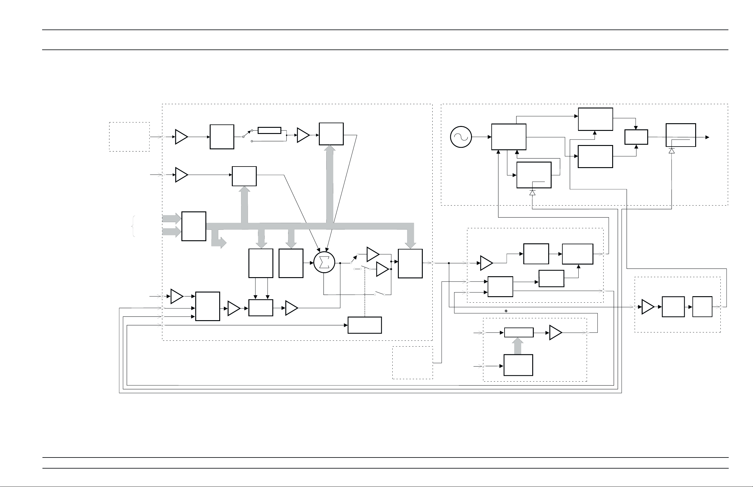
FUNCTIONAL ALC AND
DESCRIPTION MODULATION
E x t e r n a l
*
A M
( F r o m F r o n t /
R e a r P a n e l )
A L C S l o p e
( F r o m A 1 2 P C B )
F r o m
C P U
E x t e r n a l A L C
( F r o m F r o n t /
R e a r P a n e l )
D 0 - D 1 5
L _ S E L 3
A 0 1 - A 0 3
D e t e c t o r 1
D e t e c t o r 0
S a m p l e / H o l d
E P L D
D e t e c t o r
M U X
A M
I N P U T
S E N S
D A C
S w i t c h
C o n t r o l
C i r c u i t s
S L O P E
D A C
L O G A M P
D e t e c t o r
C A L
D A C
L o g
A m p
P / O A 1 0 P C B
L e v e l
R E F
D A C
A M
C A L
D A C
N o n - P u l s e
L e v e l A m p
F i x e d
G a i n
S a m p l e / H o l d
C o n t r o l
P u l s e
L e v e l A m p
A L C
G a i n
C A L
D A C
P / O R F D e c k
2 - 2 0 G H z
Y I G
O s c i l l a t o r
A L C
C o n t r o l
1 0 M H z
( F r o m
A 5 P C B )
S w i t c h e d
F i l t e r
M o d u l a t o r C o n t r o l
B u f f e r
A m p
S a m p l e /
H o l d
M U X
1 0 - 1 6 . 2 5 G H z
0 . 0 1 - 2 0 G H z
0 . 0 1 - 2 G H z
D o w n
C o n v e r t e r
D e t e c t o r 0
P / O A 9 P C B
S h a p e r /
A m p
I n t e r n a l S q u a r e W a v e
D i v i d e r s
P u l s e
L e v e l
S h i f t
D r i v e r
A L C
M o d u l a t o r
D r i v e r
S o u r c e
Q u a d r u p l e r
M o d u l e
S w i t c h e d
D o u b l e r
M o d u l e
S a m p l e /
H o l d
4 0 -
6 5 G H z
0 . 0 1 -
4 0 G H z
F o r w a r d
C o u p l e r
0 . 0 1 -
6 5 G H z
M o d u l a t o r C o n t r o l
P / O A 1 4 P C B
S h a p e r /
B u f f e r
A m p
L e v e l
D e t e c t o r
D e t e c t o r 1
A m p
T o S t e p
A t t e n u a t o r
o r
R F O u t p u t
D r i v e r /
A m p
E x t e r n a l
*
S q u a r e W a v e /
P u l s e
( F r o m F r o n t /
R e a r P a n e l )
S e r i a l D a t a
( F r o m
A 1 6 P C B )
S e r i a l /
P a r a l l e l
C o n v e r t e r
P / O A 6 P C B
6 9 1 X X B M o d e l s O n l y
*
Figure 2-3. Block Diagram of the ALC and
Modulation Subsystem
690XXB/691XXB MM 2-17
Page 46

FUNCTIONAL ALC AND
DESCRIPTION MODULATION
Power Sweep
In this mode, the CPU has the ALC step the RF out
put through a range of levels specified by the user.
This feature can be used in conjunction with the
sweep mode to produce a set of identical frequency
sweeps, each with a different RF power output level.
-
Amplitude
Modulation
(691XXB only)
Square Wave
Modulation
(691XXB only)
Amplitude modulation (AM) of the RF output signal
by an external signal is accomplished by summing
the external modulating signal into the ALC loop.
External modulating signals come from the front
panel or rear panel AM IN inputs. On the A10 PCB,
the AM Input Sensitivity DAC and the AM Calibra
tion DAC, under the control of the CPU, adjust the
modulating signal for the proper amount of AM in
both the linear (log amp in) and the log (log amp
out) modes of operation. The adjusted modulating
signal is summed with the level reference, slope,
and detector inputs into the ALC loop. This produces an ALC control signal that varies with the
modulating signal. The action of the ALC loop then
causes the envelope of the RF output signal to track
the external modulation signal.
Square wave modulation is accomplished by turning
the RF output signal on and off using internally
generated square wave or external square wave inputs.
The A6 Square Wave Generator PCB, under control
of the CPU, divides the 10 MHz reference signal
received from the A5 Fine Loop PCB to produce
square waves. These internal square wave signals
are fed to the A9 PIN Control PCB. There they are
multiplexed with the external square wave signals
received from the front or rear panel. The output of
the multiplexer is two sample/hold signals. One goes
via a pulse level shift circuit to the ALC modulator
driver to modulate the RF output signal; the other
goes to the A10 ALC PCB to cause the level ampli
fier to operate as a sample/hold amplifier. The am
plifier is synchronized with the modulating signal so
that the ALC loop effectively operates only during
the ON portion of the modulated RF output signal.
-
-
-
2-18 690XXB/691XXB MM
Page 47
FUNCTIONAL RF DECK
DESCRIPTION ASSEMBLIES
2-5 RF DECK ASSEMBLIES The primary purpose of the RF deck assembly is to generate CW and
swept frequency RF signals and route these signals to the front panel
RF OUTPUT connector. It is capable of generating RF signals in the
frequency range of 0.01 to 65 GHz (0.00001 to 65 GHz with Option 22).
The series 690XXB/691XXB synthesized CW/signal generators use a
single YIG-tuned oscillator. All other frequencies, except for 0.01 to
10 MHz, are derived from the fundamental frequencies generated by
this oscillator, as follows:
RF output frequencies of 0.01 to 2 GHz are developed by down
q
converting the fundamental frequencies of 6.51 to 8.5 GHz.
RF output frequencies of 0.01 to 2.2 GHz are developed by down-
q
converting the fundamental frequencies of 2 to 4.4 GHz using the
Digital Down Converter assembly, installed by Option 21A.
RF output frequencies of 20 to 40 GHz are produced by doubling
q
the fundamental frequencies of 10 to 20 GHz.
RF output frequencies of 40 to 65 GHz are produced by quadru-
q
pling the fundamental frequencies of 10 to 16.25 GHz.
RF output frequencies of 0.01 to 10 MHz are generated by the
q
A13 10 MHz DDS PCB, installed by Option 22.
The following paragraphs briefly describe the operation of the RF deck
assembly.
RF Deck Configurations
All 690XXB/691XXB RF deck assemblies contain a
YIG-tuned oscillator, a switched filter assembly, and
a directional coupler. Beyond that, the configuration
of the RF deck assembly varies according to the par
ticular instrument model. Block diagrams of the
various RF deck configurations are shown in the fol
lowing figures:
q
Figure 2-4, page 2-21, is a block diagram of the
RF deck assembly for Model 69017B/69117B.
q
Figure 2-5, page 2-22, is a block diagram of the
RF deck assembly for Models 69037B/69137B
and 69047B/69147B.
q
Figure 2-6, page 2-23, is a block diagram of the
RF deck assembly for Model 69067B/69167B.
q
Figure 2-7, page 2-24, is a block diagram of the
RF deck assembly for Models 69077B/69177B,
69087B/69187B, and 69097B/69197B.
-
-
-
The block diagrams of the RF deck assemblies in
clude all of the common RF components found in the
690XXB/691XXB RF deck assemblies. Refer to these
block diagrams during the descriptions of RF deck
operation presented in the following paragraphs.
-
690XXB/691XXB MM 2-19
Page 48

FUNCTIONAL RF DECK
DESCRIPTION ASSEMBLIES
YIG-tuned
Oscillator
There are two configurations of YIG-tuned oscillator
used in the 690XXB/691XXB—a 2 to 8.4 GHz oscil
lator used in the 69017B/69117B model anda2to
20 GHz oscillator used in all other 690XXB/691XXB
models. The 2 to 20 GHz YIG-tuned oscillator actu
ally contains two oscillators—one covering the fre
quency range of 2 to 8.4 GHz and one covering the
frequency range of 8.4 to 20 GHz. Both oscillators
use a common internal amplifier.
The YIG-tuned oscillator generates RF output sig
nals that have low broadband noise and low spuri
ous content. It is driven by the main tuning coil
current and bias voltages from the A14 YIG, SDM,
SQM Driver PCB and the FM tuning coil current
from the A11 FM PCB. During CW mode, the main
tuning coil current tunes the oscillator to within a
few megahertz of the final output frequency. The
phase-lock circuitry of the YIG loop then fine adjusts the oscillator's FM tuning coil current to make
the output frequency exact. In the 691XXB, frequency modulation of the RF output is also accomplished by summing the external modulating
signals into the oscillator's FM tuning coil control
path.
-
-
-
-
-
NOTE
For 691XXBs with Option 21A at
frequenciesof£2.2 GHz,broad-band
analog frequency sweeps are
>25 MHz wide; narrow-band analog
frequency sweeps are £25 MHz.
Power Level
Control and
Modulation
When the 691XXB is generating broad-band analog
frequency sweeps (>100 MHz wide), the main tuning coil current tunes the oscillator through the
sweep frequency range. Phase locking to fine adjust
the oscillator's output frequency is only done at the
bottom and top of the sweep ramp and on both sides
of each band switch point. Narrow-band analog fre
quency sweeps (£100 MHz wide) in the 691XXB are
accomplished by summing the appropriate sweep
ramp signal into the oscillator's FM tuning coil con
trol path. The YIG-tuned oscillator's RF output is
then swept about a center frequency that is set by
the main tuning coil current. Phase locking to fine
tune the output frequency is done at the center fre
quency of the sweep.
The RF output signal from the YIG-tuned oscillator
goes to connector J6 on the switched filter assembly.
In the switched filter assembly, the RF signal is
amplified then goes to the modulator. A portion of
the RF signal to the modulator is picked off and
coupled out via connector J5 to the Sampler for use
by the YIG loop circuitry.
-
-
-
2-20 690XXB/691XXB MM
Page 49

FUNCTIONAL RF DECK
DESCRIPTION ASSEMBLIES
S w i t c h e d F i l t e r A s s y . - D 4 5 1 9 4 ( S t a n d a r d )
- D 4 5 1 9 8 ( O p t i o n 1 5 A )
3 . 3 G H z L P F
5 . 5 G H z L P F
8 . 4 G H z L P F
8 . 5 G H z L P F
1 3 . 5 G H z L P F
J 3
> + 1 7 d B m
S w i t c h
C o n t r o l
D o w n C o n v e r t e r A s s y .
D 2 7 3 3 0
J 1
J 2
6 . 5 G H z
L P F
> + 1 5 d B m ( S t d . )
> + 2 0 d B m ( O p t . 1 5 A )
2 0 G H z L P F
J 1
J 3
J 2
0 . 0 1 - 2 G H z
> + 1 6 d B m
R F P a t h
w i t h
O p t i o n 2 2
L o s s A - C < 2 d B
L o s s B - C < 2 d B
R F P a t h w i t h O p t i o n 2 2
D i p l e x e r
A
2 9 8 6 0
C
B
C o n t r o l
0 . 0 0 0 0 1 - 2 G H z
D i p l e x e r
A
C
4 6 5 0 4
C o n t r o l
D i r e c t i o n a l
C o u p l e r
L e v e l
C o n t r o l
L o s s A - C < 1 . 5 d B
L o s s B - C < 1 . 5 d B
0 . 0 1 - 1 0 M H z
B
> + 1 5 d B m
S t e p
A t t e n u a t o r
( O p t i o n )
C o n t r o l
A 1 3
D D S
( O p t i o n 2 2 )
R F O u t p u t
0 . 0 1 - 8 . 4 G H z
( 0 . 0 0 0 0 1 - 8 . 4 G H z
w i t h O p t i o n 2 2 )
B I A S
M A I N
2 - 8 . 4 G H z
Y I G O s c i l l a t o r
> + 4 d B m
F M
J 6
J 5
M o d u l a t o r
C o n t r o l
S a m p l e r
( - 7 t o - 1 4 d B m
t y p i c a l )
6 . 5 1 - 8 . 5 G H z
5 0 0 M H z
L e v e l
C o n t r o l
NOTE
If the Electronic Step Attenuator (Option 2E) is installed,
the 0.01 to 10 MHz signal (Option 22) is inserted at the
Step Attenuator. Diplexers (P/Ns 29860 and 46504) are
not required.
Figure 2-4. Block Diagram of the RF Deck Assembly for
Model 69017B/69117B.
690XXB/691XXB MM 2-21
Page 50

FUNCTIONAL RF DECK
DESCRIPTION ASSEMBLIES
B I A S
M A I N
2 - 2 0 G H z
Y I G O s c i l l a t o r
8 . 4 - 2 0 G H z
F M
2 - 8 . 4 G H z
> + 4 d B m
S w i t c h e d F i l t e r A s s y . - D 4 5 1 9 4 ( S t a n d a r d )
- D 4 5 1 9 8 ( O p t i o n 1 5 A )
3 . 3 G H z L P F
J 6
J 5
S a m p l e r
( - 7 t o - 1 4 d B m
t y p i c a l )
M o d u l a t o r
C o n t r o l
6 . 5 1 - 8 . 5 G H z
J 3
5 0 0 M H z
8 . 5 G H z L P F
> + 1 7 d B m
J 1
J 2
5 . 5 G H z L P F
8 . 4 G H z L P F
1 3 . 5 G H z L P F
S w i t c h
C o n t r o l
D o w n C o n v e r t e r A s s y .
D 2 7 3 3 0
L P F
6 . 5 G H z
> + 1 5 d B m ( S t d . )
> + 2 0 d B m ( O p t . 1 5 A )
2 0 G H z L P F
J 1
J 3
J 2
L o s s A - C < 2 d B
L o s s B - C < 2 d B
0 . 0 1 - 2 G H z
> + 1 6 d B m
R F P a t h
w i t h
O p t i o n 2 2
R F P a t h w i t h O p t i o n 2 2
D i p l e x e r
A
2 9 8 6 0
C
B
C o n t r o l
0 . 0 0 0 0 1 - 2 G H z
D i p l e x e r
A
C
4 6 5 0 4
C o n t r o l
D i r e c t i o n a l
C o u p l e r
L e v e l
C o n t r o l
L o s s A - C < 1 . 5 d B
L o s s B - C < 1 . 5 d B
0 . 0 1 - 1 0 M H z
B
> + 1 5 d B m
S t e p
A t t e n u a t o r
( O p t i o n )
C o n t r o l
A 1 3
D D S
( O p t i o n 2 2 )
R F O u t p u t
0 . 0 1 - 2 0 G H z
( 0 . 0 0 0 0 1 - 2 0 G H z
w i t h O p t i o n 2 2 )
L e v e l
C o n t r o l
NOTES
1. Down Converter Assy (P/N D27330) not installed in
Model 69037B/69137B.
2. If the Electronic Step Attenuator (Option 2F) is installed,
the 0.01 to 10 MHz signal (Option 22) is inserted at the
Step Attenuator. Diplexers (P/Ns 29860 and 46504) are
not required.
Figure 2-5. Block Diagram of the RF Deck Assembly for
Models 69037B/69137B and 69047B/69147B.
2-22 690XXB/691XXB MM
Page 51

FUNCTIONAL RF DECK
DESCRIPTION ASSEMBLIES
2 0 - 4 0 G H z
> + 8 . 5 d B m
R F P a t h w i t h O p t i o n 2 2
D i p l e x e r
A
D i p l e x e r
A
2 9 8 5 0
C
B
C o n t r o l
C
B
4 6 5 0 4
D i r e c t i o n a l
C o u p l e r
L e v e l
C o n t r o l
L o s s A - C < 1 . 5 d B
L o s s B - C < 1 . 5 d B
0 . 0 1 - 1 0 M H z
> + 1 5 d B m
A 1 3
D D S
( O p t i o n 2 2 )
S t e p
A t t e n u a t o r
( O p t i o n )
C o n t r o l
R F O u t p u t
0 . 0 1 - 4 0 G H z
( 0 . 0 0 0 0 1 - 4 0 G H z
w i t h O p t i o n 2 2 )
B I A S
M A I N
2 - 2 0 G H z
Y I G O s c i l l a t o r
8 . 4 - 2 0 G H z
F M
2 - 8 . 4 G H z
> + 4 d B m
S w i t c h e d F i l t e r A s s y . - D 4 5 1 9 4 ( S t a n d a r d )
- D 4 5 1 9 8 ( O p t i o n 1 5 A )
3 . 3 G H z L P F
J 6
J 5
S a m p l e r
( - 7 t o - 1 4 d B m
t y p i c a l )
M o d u l a t o r
C o n t r o l
6 . 5 1 - 8 . 5 G H z
J 3
5 0 0 M H z
8 . 5 G H z L P F
> + 1 7 d B m
J 1
J 2
5 . 5 G H z L P F
8 . 4 G H z L P F
1 3 . 5 G H z L P F
S w i t c h
C o n t r o l
D o w n C o n v e r t e r A s s y .
D 2 7 3 3 0
L P F
6 . 5 G H z
> + 1 5 d B m ( S t d . )
2 0 G H z L P F
> + 2 0 d B m ( O p t . 1 5 A )
J 1
J 3
J 2
0 . 0 1 - 2 G H z
> + 1 6 d B m
S w i t c h e d D o u b l e r M o d u l e - D 2 8 5 4 0
2 0 - 2 5 G H z B P F
x 2
2 5 - 3 2 G H z B P F
3 2 - 4 0 G H z B P F
B i a s
R F P a t h w i t h O p t i o n 2 2
S w i t c h
C o n t r o l
L o s s A - C < 2 d B
L o s s B - C < 2 d B
0 . 0 0 0 0 1 - 2 G H z
C o n t r o l
L e v e l
C o n t r o l
Figure 2-6. Block Diagram of the RF Deck Assembly for
Model 69067B/69167B.
690XXB/691XXB MM 2-23
Page 52
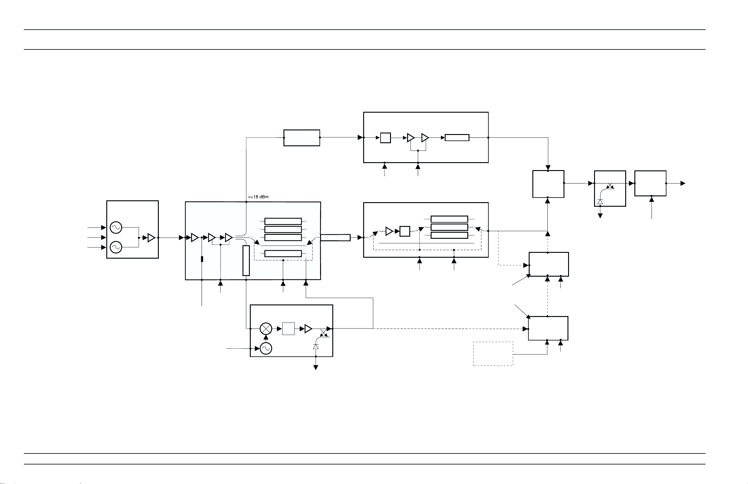
FUNCTIONAL RF DECK
DESCRIPTION ASSEMBLIES
B I A S
M A I N
B P F
S w i t c h
C o n t r o l
À
L o s s A - C < 2 d B
L o s s B - C < 2 d B
L o s s A - C < 1 . 5 d B
L o s s B - C < 1 . 5 d B
( O p t i o n 2 2 )
J 2
A 1 3
D D S
0 . 0 1 - 4 0 G H z
> + 1 0 d B m
R F P a t h
w i t h
O p t i o n 2 2
0 . 0 1 - 1 0 M H z
> + 1 5 d B m
( J 1 )
D i p l e x e r
A
D i p l e x e r
A
F o r w a r d
C o u p l e r
J 2
C
2 9 8 5 0
B
0 . 0 0 0 0 1 - 2 G H z
C
4 6 5 0 4
B
Á
C o n t r o l
C o n t r o l
J 3
D i r e c t i o n a l
C o u p l e r
C o n t r o l
S o u r c e Q u a d r u p l e r M o d u l e
À
9 0 d B
S t e p
A t t e n u a t o r
( O p t i o n )
C o n t r o lL e v e l
R F O u t p u t
0 . 0 1 - 6 5 G H z
( 0 . 0 0 0 0 1 - 6 5 G H z
w i t h O p t i o n 2 2 )
P a r t N u m b e r s :
D 2 8 1 8 5 ( 4 0 - 5 0 G H z )
6 0 - 1 4 1 ( 4 0 - 6 0 G H z )
6 0 - 1 4 2 ( 4 0 - 6 5 G H z )
Á
S Q M P / N D 2 8 1 8 5 c o n t a i n s a
F o r w a r d C o u p l e r .
F o r w a r d C o u p l e r P / N C 2 7 1 8 4 i s
u s e d w i t h S Q M P / N s 6 0 - 1 4 1 a n d
6 0 - 1 4 2 .
T h e 1 6 . 8 G H z L P F a n d 6 d B P A D ,
Â
P / N B 2 8 6 1 2 , i s u s e d w i t h
S Q M P / N s 6 0 - 1 4 1 a n d 6 0 - 1 4 2 .
S o u r c e Q u a d r u p l e r M o d u l e
J 1
Â
> + 2 0 d B m
2 0 G H z L P F
0 . 0 1 - 2 G H z
> + 1 6 d B m
J 3
x 4
J 1
B i a s
M o d u l a t o r
C o n t r o l
S w i t c h e d D o u b l e r M o d u l e - D 2 8 5 4 0
2 0 - 2 5 G H z B P F
J 2
J 1
x 2
2 5 - 3 2 G H z B P F
3 2 - 4 0 G H z B P F
B i a s
R F P a t h w i t h O p t i o n 2 2
1 6 . 8 G H z L P F
& 6 d B P A D
J 4
2 - 2 0 G H z
S w i t c h e d F i l t e r A s s y . - D 4 5 1 9 8
Y I G O s c i l l a t o r
3 . 3 G H z L P F
8 . 4 - 2 0 G H z
F M
2 - 8 . 4 G H z
> + 4 d B m
J 6
J 5
S a m p l e r
( - 7 t o - 1 4 d B m
t y p i c a l )
M o d u l a t o r
C o n t r o l
6 . 5 1 - 8 . 5 G H z
J 3
5 0 0 M H z
8 . 5 G H z L P F
> + 1 7 d B m
J 1
J 2
5 . 5 G H z L P F
8 . 4 G H z L P F
1 3 . 5 G H z L P F
S w i t c h
C o n t r o l
D o w n C o n v e r t e r A s s y .
D 2 7 3 3 0
L P F
6 . 5 G H z
L e v e l
C o n t r o l
Figure 2-7. Block Diagram of the RF Deck Assembly for
Models 69077B/69177B, 69087B/69187B, and 69097B/69197B.
2-24 690XXB/691XXB MM
Page 53

FUNCTIONAL RF DECK
DESCRIPTION ASSEMBLIES
The modulator control signal is received from the A9
PIN Control PCB where it is developed from the
ALC control signal. The modulator control signal
adjusts the gain of the modulator to control the
power level of the RF output signals. In the
691XXB, the modulator is also used for AM and
square wave modulation of the RF output signals.
Amplitude modulation is accomplished by varying
the modulator control signal with the modulating
signal. Square wave modulation is achieved by
switching the modulator on and off at a rate deter
mined by the modulating square wave.
-
RF Signal
Filtering
The RF signal from the modulator is routed via PIN
switches to the switched low-pass filters. PIN switch
drive current is received from the A9 PIN Control
PCB. A coupler in the switched filter path provides
the RF signal for the down converter. Whenever an
instrument is generating RF signals of <2 GHz
(£2.2 GHz for units with Option 21A), a RF signal is
coupled out, through a 8.5 GHz low-pass filter and
connector J3 to the down converter. Another coupler
in the switched filter path of high power switched
filter assemblies provides the RF signal for the
source quadrupler module (refer to Figure 2-7).
Whenever an instrument is generating RF signals of
>40 GHz, a RF signal is coupled out via J4 to the
source quadrupler module.
The switched low-pass filters provide rejection of the
harmonics that are generated by the YIG-tuned os
cillator. In model 69017B/69117B, the 2 to 8.4 GHz
RF signal from the moulator has three filtering
paths—3.3 GHz, 5.5 GHz, and 8.4 GHz. In all other
690XXC/691XXC models, the 2 to 20 GHz RF signal
from the modulator has four filtering paths and a
through path. The four filtering paths are 3.3 GHz,
5.5 GHz, 8.4 GHz, and 13.5 GHz. Signals above 13.5
GHz are routed via the through path.
-
After routing through the appropriate path, the 2 to
8.4 GHz or 2 to 20 GHz (2.2 GHz to 20 GHz for units
with Option 21) RF signal is multiplexed by the PIN
switches and goes via a 20 GHz low-pass filter to the
switched filter assembly output connector J2. The
0.01 to 2 GHz (0.01 to 2.2 GHz for units with Option
21A) RF signal, from the down converter, is received
at connector J1, then multiplexed through the same
path to the switched filter output J2.
690XXB/691XXB MM 2-25
Page 54

FUNCTIONAL RF DECK
DESCRIPTION ASSEMBLIES
From J2, the RF signal goes to either the directional
coupler (£20 GHz models) or the input connector J1
of the switched doubler module (>20 GHz models).
In units with Option 22, the RF signal from J2 goes
to either input connector A of the diplexer (£20 GHz
models) or the input connector J1 of the switched
doubler module (>20 GHz models).
0.01 to 2 GHz
Down
Converter
The 0.01 to 2 GHz Down Converter assembly (Fig
ures 2-4 thru 2-7) contains a 6.5 GHz VCO that is
phase-locked to the 500 MHz reference signal from
the A3 Reference Loop PCB. The 6.5 GHz VCO's
phase-lock condition is monitored by the CPU. The
6.5 GHz VCO is on at all times; however, the down
converter amplifier is powered on by the A14 YIG,
SDM, SQM Driver PCB only when the 0.01 to
2 GHz frequency range is selected.
During CW or swept frequency operations in the
0.01 to 2 GHz frequency range, the 6.51 to 8.5 GHz
RF signal output from J3 of the switched filter assembly goes to input connector J1 of the down converter. The 6.51 to 8.5 GHz RF signal is then mixed
with the 6.5 GHz VCO signal resulting in a 0.01 to
2 GHz RF signal. The resultant RF signal is fed
through a 2 GHz low-pass filter, then amplified and
routed to the output connector J3. A portion of the
down converter's RF output signal is detected, am
plified, and coupled out for use in internal leveling.
The detected RF sample is routed to the A10 ALC
PCB.
The 0.01 to 2 GHz RF output from the down con
verter goes to input connector J1 of the switched fil
ter assembly. There, the 0.01 to 2 GHz RF signal is
multiplexed into the switched filter’s output.
-
-
-
-
In units with Option 22, the 0.01 to 2 GHz RF out
put of the down converter is diplexed with the 0.01
to 10 MHz output of the A13 10 MHz DDS PCB. The
resulting 0.00001 to 2 GHz signal is then diplexed
with the RF signal from the switched filter assembly
(or switched doubler module for >20 GHz models)
into the RF path to the directional coupler.
-
2-26 690XXB/691XXB MM
Page 55

FUNCTIONAL RF DECK
DESCRIPTION ASSEMBLIES
D i g i t a l D o w n C o n v e r t e r A s s y . - 5 0 7 2 2 - 1
R F I n
2 . 0 - 4 . 4 G H z
( f r o m S w i t c h e d F i l t e r
P o r t J 3 )
J 1
n
2
¸
( n = 1 t o 8 )
R F S w i t c h
C o n t r o l s
D i g i t a l C o n t r o l
( f r o m A 1 4 P C B )
P 1
Figure 2-8. Digital Down Converter (Option 21A)
0.01 to 2.2 GHz
Digital Down
Converter
P 1
L e v e l
C o n t r o l
( f r o m
A 9 P C B )
J 6
L e v e l
D e t e c t o r
J 3
R F O u t
0 . 0 1 - 2 . 2 G H z
> + 1 7 d B m
( t o S w i t c h e d F i l t e r
P o r t J 1 )
L P F s
1 6 B a n d s
The 0.01 to 2.2 GHz Digital Down Converter assembly (Figure 2-8), found in units with Option 21A,
provides improved phase noise across the 0.01 to
2.2 GHz frequency range. Power is supplied to the
digital down converter assembly at all times; however, the down converter amplifiers are powered on
by the A14 YIG, SDM, SQM Driver PCB only when
the 0.01 to 2.2 GHz frequency range is selected.
During CW or swept frequency operations in the
0.01 to 2.2 GHz frequency range, the 2 to 4.4 GHz
RF signal output from J3 of the switched filter as
sembly goes to input connector J1 of the digital
down converter. In the down converter, the 2 to
4.4 GHz RF signal is divided by 2
n
, wheren=1to8.
From the frequency dividers, the resulting 0.01 to
2.2 GHz RF signal is amplified, then goes to the
modulator which provides power level control.
The level control signal is received from the A9 PIN
Control PCB where it is developed from the ALC
control signal. The level control signal adjusts the
gain of the modulator to control the power level of
the RF output signals. In the 691XXB, the modula
tor is also used for AM and square wave modulation
of the RF output signals. Amplitude modulation is
accomplished by varying the level control signal
with the modulating signal. Square wave modula
-
tion is achieved by switching the modulator on and
690XXB/691XXB MM 2-27
Page 56

FUNCTIONAL RF DECK
DESCRIPTION ASSEMBLIES
off at a rate determined by the modulating square
wave.
The 0.01 to 2.2 GHz RF signal from the modulator is
amplified and routed via PIN switches to the
switched low-pass filters. PIN switch drive current
is generated by internal drivers that are controlled
by signals received from the A12 Analog Instruction
PCB via the A14 PCB. There are 16 switched lowpass filters covering the 0.01 to 2.2 GHz frequency
range. These low-pass filters provide rejection of un
wanted harmonics. After routing through the appro
priate filter path, the 0.01 to 2.2 GHz RF signal is
multiplexed by PIN switches to the output connec
tor J3. A portion of the down converter’s RF output
signal is detected, amplified, and coupled out for use
in internal leveling. The detected RF sample is
routed to the A10 ALC PCB.
-
-
-
Switched
Doubler
Module
The 0.01 to 2.2 GHz output from the digital down
converter goes to input connector J1 of the switched
filter assembly. There, the 0.01 to 2.2 GHz RF signal
is multiplexed into the switched filter’s output path.
In units with Option 22, the 0.01 to 2.2 GHz RF output of the digital down converter is diplexed with
the 0.01 to 10 MHz output of the A13 10 MHz DDS
PCB. The resulting 0.00001 to 2.2 GHz signal is
then diplexed with the RF signal from the swtiched
filter assembly (or switched doubler module for
>20 GHz models) into the RF path to the directional
coupler.
The switched doubler module (SDM), found in
>20 GHz models is used to double the fundamental
frequencies of 10 to 20 GHz to produce RF output
frequencies of 20 to 40 GHz.
The RF signal from the switched filter assembly is
input to the SDM at J1. During CW or swept fre
quency operations in the 20 to 40 GHz frequency
range, the 10 to 20 GHz RF signal input is routed by
PIN switches to the doubler/amplifiers. PIN switch
drive current is provided by the A9 PCB and bias
voltage for the doubler/amplifiers is supplied by the
A14 YIG, SDM, SQM Driver PCB. The RF signal is
amplified, then doubled in frequency. From the dou
bler, the 20 to 40 GHz RF signal is routed by PIN
switches to the bandpass filters. There are three
bandpass filter paths to provide good harmonic per
-
-
-
2-28 690XXB/691XXB MM
Page 57

FUNCTIONAL RF DECK
DESCRIPTION ASSEMBLIES
formance. The frequency ranges of the three paths
are 20 to 25 GHz, 25 to 32 GHz, and 32 to 40 GHz.
Source
Quadrupler
Module
After routing through the appropriate bandpass fil
ter path, the 20 to 40 GHz RF signal is multiplexed
by the PIN switches to the SDM output at connector
J2. RF signals input to the SDM of £20 GHz are
multiplexed through by the PIN switches to output
connector J2.
From J2, the RF signal goes to either the directional
coupler (£40 GHz models) or the input connector J2
of the forward coupler (>40 GHz models).
In units with Option 22, the RF signal from J2 goes
to input connector A of the diplexer where it is di
plexed with the 0.00001 to 2 GHz RF signal (from
the down converter and A13 10 MHz DDS PCB) into
the RF path to either the directional coupler
(£40 GHz models) or the input connector J2 of the
forward coupler (>40 GHz models).
The source quadrupler module (SQM), found in
>40 GHz models, is used to quadruple the fundamental frequencies of 10 to 16.25 GHz to produce
RF output frequencies of 40 to 65 GHz. The RF signal inputs for the SQM come from the switched filter assembly. The modulator control signal for the
SQM is received from the A14 YIG, SDM, SQM
Driver PCB where it is developed from the ALC control signal. The A14 PCB also supplies the amplifier
bias voltage(s) for the SQM.
-
-
Model 69077B/69177B (SQM P/N D28185)
During CW and swept frequency operations in the
40 to 50 GHz frequency range, the 10 to 12.5 GHz
RF signal input is quadrupled and amplified, then
goes to the modulator. The modulator provides for
power level control and, in the 69177B, amplitude
modulation of the RF output signals. From the
modulator, the 40 to 50 GHz RF signals goes via a
band-pass filter to output connector J3 of the for
ward coupler. Note that on the 40 to 50 GHz SQM
(P/N D28185), the forward coupler is an integral
part of the SQM. The 0.01 to 40 GHz RF output sig
nals from the SDM (0.00001 to 40 GHz RF output
signals from the diplexer for 69077B/69177Bs with
Option 22) are routed to input connector J2 of the
SQM forward coupler. The 0.01 to 50 GHz (0.00001
to 50 GHz for 69077B/69177Bs with Option 22) RF
output signals go from J3 of the SQM forward cou
pler to the directional coupler.
-
-
690XXB/691XXB MM 2-29
-
Page 58

FUNCTIONAL RF DECK
DESCRIPTION ASSEMBLIES
Model 69087B/69187B (SQM P/N 60-141)
During CW or swept frequency operations in the 40
to 60 GHz frequency range, the 10 to 15 GHz RF
signal input is quadrupled and amplified, then goes
to the modulator. The modulator provides for power
level control and, in the 69187B, amplitude modula
tion of the RF output signal. From the modulator,
the 40 to 60 GHz RF signals go via a band-pass fil
ter to the output connector of the SQM.
From the SQM, the 40 to 60 GHz RF output signals
go to the input connector J1 of the forward coupler,
P/N C27184. The other input to the forward coupler
at connector J2 is the 0.01 to 40 GHz RF output sig
nal from the SDM (0.00001 to 40 GHz RF output
signals from the diplexer for 69087B/69187Bs with
Option 22). From forward coupler output connector
J3, the 0.01 to 60 GHz (0.00001 to 60 GHz for
69087B/69187Bs with Option 22) RF output signals
go to the directional coupler.
-
-
-
Power Level
Detection/
ALC Loop
Model 69097B/69197B (SQM P/N 60-142)
During CW or swept frequency operations in the 40
to 65 GHz frequency range, the 10 to 16.25 GHz RF
signal input is qaudrupled and amplified, then goes
to the modulator. The modulator provides for power
level control and, in the 69197B, amplitude modulation of the RF output signals. From the modulator,
the 40 to 65 GHz RF signals go via a band-pass fil
ter to the output connector of the SQM.
From the SQM, the 40 to 65 GHz RF output signals
go to the input connector J1 of the forward coupler,
P/N C27184. The other input to the forward coupler
at connector J2 is the 0.01 to 40 GHz RFoutput sig
nals from the SDM (0.00001 to 40 GHz RF output
signals from the diplexer for 69097B/69197Bs with
Option 22). From forward coupler output connector
J3, the 0.01 to 65 GHz (0.00001 to 65 GHz for
69097B/69197Bs with Option 22) RF output signals
go to the directional coupler.
The RF output signal from either the switched filter
(£20 GHz models), the SDM (£40 GHz models), the
diplexer (£20 GHz and £40 GHz models with Option
22), or the forward coupler (>40 GHz models) goes to
the directional coupler for transfer to the RF OUT
PUT connector. A portion of the RF output signal is
detected and coupled out as feedback to the ALC cir
cuitry on the A10 ALC PCB. In these circuits, the
signal from the detector is summed with the refer
-
-
-
-
-
2-30 690XXB/691XXB MM
Page 59

FUNCTIONAL RF DECK
DESCRIPTION ASSEMBLIES
ence voltage that represents the desired RF output
power level. The resulting voltage is fed from the
A10 PCB to the ALC modulator driver circuit on the
A9 PIN Control PCB (and the ALC modulator driver
circuit on the A14 YIG, SDM, SQM Driver PCB for
>40 GHz models). The modulator control signals go
to the modulators in the switched filter assembly
and the SQM (for >40 GHz models) to adjust the RF
output power level.
Step
Attenuators
The optional step attenuators available for use with
the 690XXB/691XXB models are as follows:
120 dB electronic step attenuators for
q
£8.4 GHz and £20 GHz models (Options 2E
and 2F)
110 dB step attenuators for £20 GHz and
q
£40 GHz models (Options 2A and 2B)
90 dB step attenuators for £50 GHz and
q
£60 GHz models (Option 2C and 2D)
The step attenuators provide attenuation of the RF
output in 10 dB steps. The step attenuator drive
current is supplied by the A9 Control PCB.
690XXB/691XXB MM 2-31/2-32
Page 60

Page 61

Chapter 3
Performance Verification
Table of Contents
3-1 INTRODUCTION
3-2 RECOMMENDED TEST EQUIPMENT
3-3 TEST RECORDS
3-4 CONNECTOR AND KEY LABEL NOTATION
3-5 690XXB/691XXB POWER LEVELS .........3-6
3-6 INTERNAL TIME BASE AGING RATE TEST . . . 3-7
Test Setup ....................3-7
Test Procedure..................3-8
3-7 FREQUENCY SYNTHESIS TESTS ........3-10
Test Setup ...................3-10
Coarse Loop/YIG Loop Test Procedure......3-10
Fine Loop Test Procedure ............3-11
3-8 SPURIOUS SIGNALS TEST: RF OUTPUT
SIGNALS £2 GHz (£2.2 GHz UNITS
W/OPTION 21A)
Test Setup
0.01 - 2 GHz Test Procedure
0.01 - 2.2 GHz Test Procedure
...................
...................
.......
...................
...
..................
..........
..........
3-3
3-3
3-3
3-3
3-12
3-12
3-12
3-15
3-9 HARMONIC TEST: RF OUTPUT SIGNALS
FROM2TO20GHz
Test Setup
2 - 10 GHz Test Procedure
11 - 20 GHz Test Procedure
3-10 SINGLE SIDEBAND PHASE NOISE TEST
Test Setup
Test Procedure
...................
...................
.................
................
...........
..........
....
3-16
3-16
3-17
3-18
3-20
3-20
3-21
Page 62

Table of Contents (Continued)
3-11 POWER LEVELACCURACY AND FLATNESS
TESTS
Test Setup
Power Level Accuracy Test Procedure
Power Level Flatness Test Procedure
........................
...................
......
......
3-24
3-24
3-25
3-26
3-12 AMPLITUDE MODULATION TEST
Test Setup
AM Input Sensitivity Procedure
3-13 FREQUENCY MODULATION TESTS
Test Setup
FM Input Sensitivity Procedure.........3-32
...................
.........
...................
........
.......
3-28
3-28
3-29
3-31
3-31
Page 63

Chapter 3
Performance Verification
3-1 INTRODUCTION This chapter contains tests that can be used to verify the performance
of the Series 690XXB/691XXB Synthesized CW/Signal Generators to
specifications. These tests support all instrument models having any
version of firmware. Units with Option 2A, 2B, 2C, 2D, 2E, and 2F
(110 dB, 90 dB, and 120 dB step attenuators), Option 11 (0.1 Hz fre
quency resolution), Option 15A (high power output), and Option 21A
(digital down converter) are also covered.
-
3-2 RECOMMENDED TEST
EQUIPMENT
Table 3-1 (page 3-4) provides a list of the recommended test equipment
for the performance verification tests.
The test procedures refer to specific test equipment front panel control
settings when the test setup is critical to making an accurate measurement. In some cases, the user may substitute test equipment having the same critical specifications as those on the recommended test
equipment list.
Contact your local Anritsu service center (refer to Table 1-5 on page
1-18) if you need clarification of any equipment or procedural reference.
3-3 TEST RECORDS Ablank copy of a sample performance verification test record for each
690XXB/691XXB model is provided in Appendix A. Each test record
contains the model-specific variables called for by the test procedures.
It also provides a means for maintaining an accurate and complete
record of instrument performance. We recommend that you copy these
pages and use them to record the results of your initial testing of the
instrument. These initial test results can later be used as benchmark
values for future tests of the same instrument.
3-4 CONNECTOR AND KEY
LABEL NOTATION
The test procedures include many references to equipment intercon
nections and control settings. For all 690XXB/691XXB references, spe
cific labels are used to denote the appropriate menu key, data entry
key, data entry control, or connector (such as CW/SWEEP SELECT or
RF OUTPUT). Most references to supporting test equipment use gen
eral labels for commonly used controls and connections (such as Span
or RF Input). In some cases, a specific label is used that is a particular
feature of the test equipment listed in Table 3-1.
-
-
-
690XXB/691XXB MM 3-3
Page 64

PERFORMANCE RECOMMENDED
VERIFICATION TEST EQUIPMENT
Table 3-1. Recommended Test Equipment for Performance Verification Tests (1 of 2)
INSTRUMENT
Spectrum Analyzer,
with
External Mixers
and
Diplexer Assy
Phase Noise
Measurement
System
Frequency Counter Frequency Range: 0.01 to 40 GHz
Power Meter,
with
Power
Sensors
Frequency Reference Frequency: 10 MHz
Function Generator Output Voltage: 2 volts peak-to-peak
Modulation Analyzer Frequency Input: 10 MHz
Attenuator Frequency Range: DC to 40 GHz
Attenuator Frequency Range: DC to 40 GHz
Attenuator Frequency Range: DC to 60 GHz
Frequency Resolution: 0.01 to 65 GHz
Resolution Bandwidth: 10 Hz
Frequency Range: 5 MHz to 26.5 GHz Aeroflex/Comstron PN9000
Input Impedance: 50
Resolution: 1Hz
Other: External Time Base Input
Power Range: –30 to +20 dBm
Accuracy: 5x10
Functions: 0.1 Hz to 100 kHz sine and
square waveforms
(or the IF of the spectrum analyzer)
AM Depth: 0% to 90%
AM Modulation Rates: DC to 100 kHz
Filters: 20 kHz lowpass, 300 Hz highpass
Max Input Power: >+17 dBm
Attenuation: 10 dB
Max Input Power: >+17 dBm
Attenuation: 20 dB
Max Input Power: >+17 dBm
Attenuation: 10 dB
CRITCAL
SPECIFICATION
W
(1mW to 100mW)
–12
parts/day
RECOMMENDED
MANUFACTURER/MODEL
Tektronix, Model 2794, with
External Mixers:
WM780K (18 to 26.5 GHz)
WM780A (26.5 to 40 GHz)
WM780U (40 to 60 GHz)
WM780E (60 to 90 GHz)
and
Diplexer Assy: 015-385-00
with
PN9060-00 Status Module
PN9470-00 Noise Output Module
PN9450-00 Lock Control Module
PN9342-01 Phase Detector Module
PN9530-00 Crystal Oscillator Module
Anritsu Model MF2414A 3-7
Anritsu Model ML2437A or ML2438A,
with
Power Sensors:
MA2474A (0.01 to 40 Ghz)
MA2475A (0.01 to 50 GHz)
Absolute Time Corp., Model 300 3-6
Hewlett-Packard, Model 33120A 3-12, 3-13
Hewlett-Packard, Model 8901A 3-12
Anritsu, Model 41KC-10 3-9, 3-10
Anritsu, Model 41KC-20 3-9
Anritsu, Model 41V-10 3-9, 3-10
TEST
NUMBER
3-8, 3-9
3-10
3-11
3-4 690XXB/691XXB MM
Page 65

PERFORMANCE RECOMMENDED
VERIFICATION TEST EQUIPMENT
Table 3-1. Recommended Test Equipment for Performance Verification Tests (2 of 2)
INSTRUMENT
Attenuator Frequency Range: DC to 60 GHz
Max Input Power: >+17 dBm
Attenuation: 20 dB
Special AUX I/O
Cable Assy.
Tee Connectors: 50WBNC Any common source 3-10
Cables Connectors: 50WBNC Any common source All tests
Provides interface between the 690XXB/
691XXB and the Power Meter
CRITCAL
SPECIFICATION
Anritsu, Model 41V-20 3-9
Anritsu P/N: 806-90 3-11
RECOMMENDED
MANUFACTURER/MODEL
TEST
NUMBER
690XXB/691XXB MM 3-5
Page 66

PERFORMANCE 690XXB/691XXB
VERIFICATION POWER LEVELS
3-5 690XXB/691XXB POWER
LEVELS
Table 3-2, page 3-6, is a listing of the Series 690XXB and 691XXB Syn
thesized CW/Signal Generator models and their maximum leveled ou
put power levels. Certain test procedures will refer you to this table
for the maximum leveled output power level setting of the instrument
model being tested.
Table 3-2. 690XXB/691XXB Maximum Leveled Output Power
69XXXB
Model
69X17B 0.01 – 8.4 GHz +13.0 dBm +11.0 dBm +9.0 dBm
69X37B 2.0 – 20.0 GHz +13.0 dBm +11.0 dBm +3.0 dBm
69X47B 0.01 – 20.0 GHz +13.0 dBm +11.0 dBm +3.0 dBm
69X67B
69X77B
69X87B
69X97B
Frequency
(GHz)
0.01 – 2.0 GHz
2.0 – 20.0 GHz
20.0 – 40.0 GHz
0.01 – 2.0 GHz
2.0 – 20.0 GHz
20.0 – 40.0 GHz
40.0 – 50.0 GHz
0.01 – 2.0 GHz
2.0 – 20.0 GHz
20.0 – 40.0 GHz
40.0 – 50.0 GHz
50.0 – 60.0 GHz
0.01 – 2.0 GHz
2.0 – 20.0 GHz
20.0 – 40.0 GHz
40.0 – 50.0 GHz
50.0 – 65.0 GHz
Max Leveled
Output Power
+13.0 dBm
+9.0 dBm
+6.0 dBm
+12.0 dBm
+10.0 dBm
+2.5 dBm
+2.5 dBm
+12.0 dBm
+10.0 dBm
+2.5 dBm
+2.0 dBm
+2.0 dBm
+12.0 dBm
+10.0 dBm
+2.5 dBm
0.0 dBm
–2.0 dBm
Max Leveled
Output Power
w/Step Attenuator
+11.0 dBm
+7.0 dBm
+3.0 dBm
+10.0 dBm
+8.5 dBm
0.0 dBm
–1.0 dBm
+10.0 dBm
+8.5 dBm
0.0 dBm
–1.5 dBm
–2.0 dBm
Not Available Not Available
Step Attenuator
-
-
Max Leveled
Output Power
w/Electronic
Not Available
Not Available
Not Available
With Option 15A (High Power) Installed
69X17B
69X37B 2.0 – 20.0 GHz +17.0 dBm +15.0 dBm +7.0 dBm
69X47B
69X67B
69X77B 0.01 – 50.0 GHz Standard Standard Not Available
69X87B 0.01 – 60.0 GHz Standard Standard Not Available
69X97B 0.01 – 65.0 GHz Standard Not Available Not Available
Note: In models with Option 22 that have a high-end frequency of£20 GHz, rated output power is reduced by 1 dB.
In models with Option 22 that have a high-end frequency of >20 GHz, rated output power is reduced by 2 dB.
0.01 – 2.0 GHz
2.0 – 8.4 GHz
0.01 – 2.0 GHz
2.0 – 20.0 GHz
0.01 – 2.0 GHz
2.0 – 20.0 GHz
20.0 – 40.0 GHz
+13.0 dBm
+17.0 dBm
+13.0 dBm
+17.0 dBm
+13.0 dBm
+13.0 dBm
+6.0 dBm
+11.0 dBm
+15.0 dBm
+11.0 dBm
+15.0 dBm
+11.0 dBm
+11.0 dBm
+3.0 dBm
+11.0 dBm
+11.0 dBm
+11.0 dBm
+7.0 dBm
Not Available
3-6 690XXB/691XXB MM
Page 67
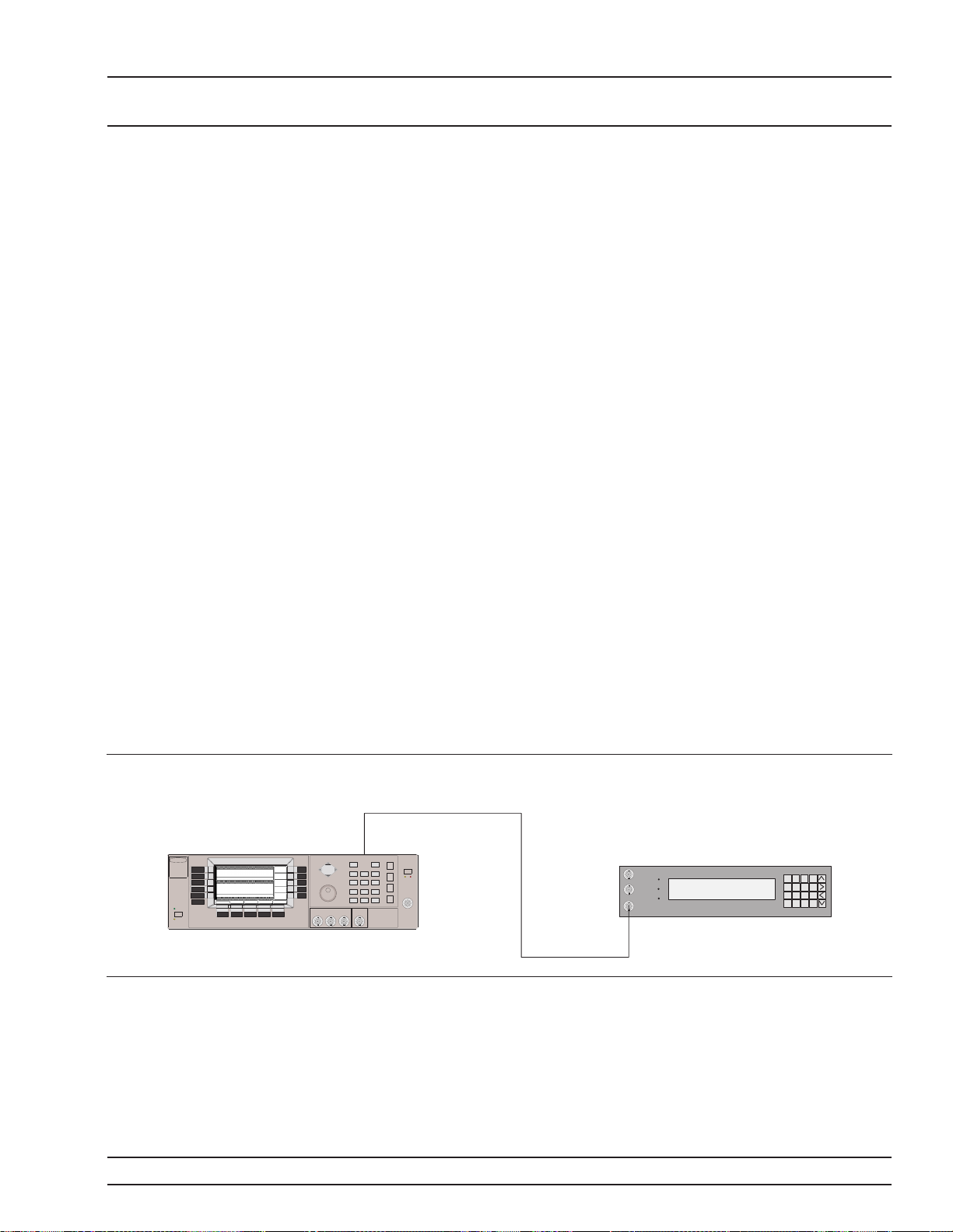
PERFORMANCE INTERNAL TIME BASE
VERIFICATION AGING RATE TEST
3-6 INTERNAL TIME BASE
AGING RATE TEST
(Optional)
The following test can be used to verify that the 690XXB/691XXB
10 MHz time base is within its aging specification.The instrument de
rives its frequency accuracy from an internal 100 MHz crystal oscilla
tor standard. (With Option 16 installed, frequency accuracy is derived
from an internal high-stability 10 MHz crystal oscillator.) An inherent
characteristic of crystal oscillators is the effect of crystal aging within
the first few days to weeks of operation. Typically, the crystal oscilla
tor's frequency increases slightly at first,then settles to a relatively
constant value for the rest of its life. The 690XXB/691XXB reference
oscillator aging is specified as <2x10
–8
parts per day (<5x10
–10
with
Option 16).
NOTES
Do not confuse crystal aging with other short term
frequency instabilities; i.e., noise and temperature. The
internal time base of the instrument may not achieve its
specified aging rate before the specified warm-up time of
7 to 30 days has elasped;therefore, this performance test is
optional.
For greatest absolute frequency accuracy, allow the 690XXB/691XXB
to warm up until its RF output frequency has stabilized (usually 7 to
30 days). Once stabilized,the change in reference oscillator frequency
should remain within the aging rate if; (1) the time base oven is not allowed to cool, (2) the instrument orientation with respect to the earth's
magnetic field is maintained, (3) the instrument does not sustain any
mechanical shock, and (4) ambient temperature is held constant. This
test should be performed upon receipt of the instrument and again after a period of several days to weeks to fully qualify the aging rate.
-
-
6 9 0 X X B / 6 9 1 X X B
1 0 M H z
R E F O U T
Figure 3-1. Equipment Setup for Internal Time Base Aging Rate Test
Test Setup
Connect the 690XXB/691XXB rear panel 10 MHz
REF OUT to the Frequency Reference front panel
input connector labeled 10 MHz when directed to do
so during the test procedure.
F r e q u e n c y R e f e r e n c e
1 P P S
1 .5 M H z
1 0 M H z
A B S O L U T E T I M E
M o d e l 3 0 0 F r e q u e n c y R e f e r e n c e
1 0 M H z I n p u t
E S C
1
-
4 5
D E L
789
M O D
.
2
3
6
E N T ER
0
690XXB/691XXB MM 3-7
Page 68

PERFORMANCE INTERNAL TIME BASE
VERIFICATION AGING RATE TEST
Test
Procedure
The frequency error is measured at the start and
finish of the test time period of 24 hours. The aging
rate is the difference between the two error read
ings.
1. Set up the Frequency Reference as follows:
a. Press the ESC key until the MAIN MENU is
displayed.
b. At the MAIN MENU display, press 1 to select
CONFIGURATION.
c. At the CONFIGURATION MENU display,
press 8 to select MEAS.
d Press the MOD key and use the Up/Down Ar
row keys to get to the menu display:
MEASUREMENT = FREQ.
e. Press the ENTER key.
f. Press the ESC key until the MAIN MENU is
displayed.
g. At the MAIN MENU display, press 3 to select
the REVIEW MENU.
h. At the REVIEW MENU display, press 8 to se-
lect TFM.
-
-
2. Connect the 690XXB/691XXB rear panel 10 MHz
REF OUT signal to the Frequency Reference front
panel 10 MHz input.
3. Wait approximately 90 minutes (default setting)
until the FMFOM on the Frequency Reference
display decreases from 9 to 1.(The default setting
is recommended to achieve optimum meas
urements.)
The frequency error in the signal under test is
displayed in ps/s (Picosecond/Second). For exam
ple, an error of –644681 ps/s is –644681 ´ 10
–6.44681 ´ 10
reference of the Frequency Reference.
The frequency error display is continuously up
dated as a running 5000-second average. The av
eraging smooths out the short-term instability of
the oscillator.
–7
away from the 10 MHz internal
-
–12
-
or
-
3-8 690XXB/691XXB MM
Page 69

PERFORMANCE INTERNAL TIME BASE
VERIFICATION AGING RATE TEST
4. Record the frequency error value,displayed on
the Frequency Reference, on the Test Record.
5. Wait for 24 hours, then record the current fre
quency error value on the Test Record.
6. The aging rate is the difference between the two
frequency error values.
7. Record the computed result on the Test Record.
To meet the specification, the computed aging
rate must be <2 ´ 10
day with Option 16).
–8
per day (<5 ´ 10
–10
-
per
690XXB/691XXB MM 3-9
Page 70

PERFORMANCE FREQUENCY
VERIFICATION SYNTHESIS TESTS
3-7 FREQUENCY SYNTHESIS
TESTS
The following tests can be used to verify correct operation of the fre
quency synthesis circuits. Frequency synthesis testing is divided into
two parts—coarse loop/YIG loop tests and fine loop tests.
6 9 0 X X B / 6 9 1 X X B
1 0 M H z
R E F O U T
R F O U T
Figure 3-2. Equipment Setup for Frequency Synthesis Tests
Test Setup
-
F R E Q U E N C Y C O U N T E R
1 0 M H z
E X T I N
I n p u t 1
Connect the equipment, shown in Figure 3-2, as follows:
1. Connect the 690XXB/691XXB rear panel 10 MHz
REF OUT to the Frequency Counter 10 MHz External Reference input.
Coarse Loop/
YIG Loop Test
Procedure
2. Connect the 690XXB/691XXB RF OUTPUT to the
Frequency Counter RF Input 1.
The following procedure tests both the coarse loop
and YIG loop by stepping the instrument through
its YIG-tuned oscillator’s frequency range in 1 GHz
steps and measuring the RF output at each step.
1. Set up the 690XXB/691XXB as follows:
a.
Reset the instrument by pressing SYSTEM ,
then Reset . Upon reset, the CW Menu is dis
played.
Press Edit F1 to open the current frequency
b.
parameter for editing.
c. Set F1 to the first test frequency indicated on
the Test Record for the model being tested.
-
3-10 690XXB/691XXB MM
Page 71

PERFORMANCE FREQUENCY
VERIFICATION SYNTHESIS TESTS
2. Record the Frequency Counter reading on the
Test Record. The Frequency Counter reading
NOTE
The Frequency Counter reading is
typically within ±1 Hz because the
instruments use a common time
base. Differences of a few Hertz can
becausedbynoiseorcounterlimita
tions. Differences of ³±100 Hz indi
catea frequencysynthesisproblem.
-
-
must be within ±100 Hz of the displayed 690XXB/
691XXB frequency to accurately complete this
test.
3. On the 690XXB/691XXB, use the cursor control
key (diamond-shaped key) to increment F1 to the
next test frequency on the Test Record. Record
the Frequency Counter reading on the Test Re
cord.
4. Repeat step 3 until all frequencies listed on the
Test Record have been recorded.
-
Fine Loop Test
Procedure
The following procedure tests the fine loop by step
ping the instrument through ten 1 kHz steps (ten
100 Hz steps for instruments with Option 11) and
measuring the RF output at each step.
1. Set up the 690XXB/691XXB as follows:
a.
Reset the instrument by pressing SYSTEM ,
then Reset . Upon reset, the CW Menu is displayed.
b. Press Edit F1 to open the current frequency
parameter for editing.
c. Set F1 to the first test frequency indicated on
the Test Record.
2. Record the Frequency Counter reading on the
Test Record. The Frequency Counter reading
must be within ±100 Hz of the displayed
690XXB/691XXB frequency (±10 Hz for instru
ments with Option 11) to accurately complete this
test.
3. On the 690XXB/691XXB, use the cursor control
key (diamond-shaped key) to increment F1 to the
next test frequency on the Test Record. Record
the Frequency Counter reading on the Test Re
cord.
-
-
-
4. Repeat step 3 until all frequencies listed on the
Test Record have been recorded.
690XXB/691XXB MM 3-11
Page 72

PERFORMANCE SPURIOUS SIGNALS TEST: RF OUTPUT SIGNALS
VERIFICATION £2 GHz (£2.2 GHz UNITS W/OPTION 21A)
3-8 SPURIOUS SIGNALS
TEST: RF OUTPUT
SIGNALS £2 GHz
(£2.2 GHz UNITS
W/OPTION 21A)
6 9 0 X X B / 6 9 1 X X B
1 0 M H z
R E F O U T
The following test can be used to verify that the CW/signal generator
meets it spurious signal specifications for RF output signals from 0.01
to 2 GHz (0.01 to 2.2 GHz for units with Option 21A). This test is ap
plicable only to instruments which cover the frequency range 10 MHz
to 2 GHz (10 MHz to 2.2 GHz for units with Option 21A). The 0.01 to
2 GHz test procedure begins on this page; the 0.01 to 2.2 GHz test pro
cedure begins on page 3-15.
S p e c t r u m A n a l y z e r
E X T R E F
I N P U T
R F I N
R F O U T
-
-
Figure 3-3. Equipment Setup for Spurious Signals Test: RF Output Signals <2 GHz
Test Setup
0.01 - 2 GHz
Test
Procedure
Connect the equipment, shown in Figure 3-3, as follows:
1. Connect the 690XXB/691XXB rear panel 10 MHz
REF OUT to the Spectrum Analyzer External Ref
erence Input.
2. Connect the 690XXB/691XXB RF OUTPUT to the
Spectrum Analyzer RF Input.
The following procedure lets you measure the worst
case spurious signals (harmonic and non-harmonic)
of the 0.01 to 2 GHz RF output to verify that they
meet specifications.
1. Set up the Spectrum Analyzer as follows:
a. Span: 10 MHz/div
b. CF: 50 MHz
c. RBW: 1 MHz
d. Sweep Time/Div: Auto (to resolve signal peaks
clearly)
-
3-12 690XXB/691XXB MM
Page 73

PERFORMANCE SPURIOUS SIGNALS TEST: RF OUTPUT SIGNALS
VERIFICATION £2 GHz (£2.2 GHz UNITS W/OPTION 21A)
2. Set up the 690XXB/691XXB as follows:
a.
Reset the instrument by pressing SYSTEM ,
then Reset . Upon reset the CW Menu is dis
played.
Press Edit L1 to open the current power level
b.
parameter for editing.
-
Table 3-3. Spurious Signals Specifications
Harmonic and Harmonic Related:
10 MHz to <100 MHz (Option 21A): <–40 dBc
³
100 MHz to£2.2 GHz (Option 21A): <–50 dBc
10 MHz to£50 MHz: <–30 dBc
>50 MHz to <2 GHz: <–40 dBc
³
2 GHz (2.2 GHz w/Option 21A)
to£20 GHz: <–60 dBc
>20 GHz to£40 GHz: <–40 dBc
Harmonic and Harmonic Related (Models having a
high-end frequency of >40 GHz and units with Option 15A at maximum specified leveled output
power):
10 MHz to <100 MHz (Option 21A): <–40 dBc
³
100 MHz to£2.2 GHz (Option 21A): <–50 dBc
10 MHz to£50 MHz: <–30 dBc
>50 Mhz to <2 GHz: <–40 dBc
³
2 GHz (2.2 GHz w/Option 21A)
to£20 GHz: <–50 dBc
>20 GHz to£40 GHz: <–40 dBc
50 GHz units: >40 GHz to£50 GHz: <–40 dBc
60 GHz units: >40 GHz to£60 GHz: <-30 dBc
65 GHz units: >40 GHz to£44 GHz: <–25 dBc
>44 GHz to£65 GHz: <-30 dBc
Non-Harmonics:
10 MHz to£2.2 GHz (Option 21A): <–60 dBc
10 MHz to <2 GHz: <–40 dBc
³
2 GHz to£65 GHz: <–60 dBc
c. Set L1 to the lesser of +10 dBm or the maxi
mum leveled power level for the instrument
being tested (refer to Table 3-2, page 3-6).
Press Edit F1 to open the current frequency
d.
parameter for editing.
e. Set F1 to 10 MHz.
3. On the Spectrum Analyzer, measure the worst
case harmonic and non-harmonic signals for the
10 MHz carrier. Record their presence by entering the levels on the Test Record. Refer to Table
3-3 for the specified level limits.
NOTE
Harmonics appear at multiples of the CW
frequency and diminish quickly as the CW
frequency gets greater than 1 GHz.
4. Repeat step 3 with F1 set first to 20 MHz, then
set to 30 MHz. Measure the worst case harmonics
and non-harmonics for each carrier frequency
and record their presence by entering their levels
on the Test Record.
5. Change the Spectrum Analyzer setup as follows:
a. Span: 100 MHz/div
b. CF: 500 MHz
6. Repeat step 3 with F1 set to 40 MHz. Measure
the worst case harmonic and non-harmonic sig
nals for the 40 MHz carrier and record their pres
ence by entering their levels on the Test Record.
-
7. Change the Spectrum Analyzer setup as follows:
a. Span: 200 MHz/div (or maximum span width)
b. CF: 1 GHz (N/A if at maximum span width)
8. Repeat step 3 with F1 set to 350 MHz. Measure
the worst case harmonic and non-harmonic sig
-
nals for the 350 MHz carrier and record their
690XXB/691XXB MM 3-13
Page 74

PERFORMANCE SPURIOUS SIGNALS TEST: RF OUTPUT SIGNALS
VERIFICATION £2 GHz (£2.2 GHz UNITS W/OPTION 21A)
presence by entering their levels on the Test Re
cord.
9. Set F1 to 1.6 GHz. Measure the worst case nonharmonic signal for the 1.6 GHz carrier and rec
ord its presence by entering its level on the Test
Record.
10. Change the Spectrum Analyzer setup as follows:
a. Span: 10 MHz/div
b. CF: 1.6 GHz
c. RBW: 1 MHz
11. Adjust the Spectrum Analyzer Reference Level
control to place the signal at the top of the screen
graticule.
12. Change the Spectrum Analyzer CF first to
3.2 GHz, then to 4.8 GHz. Compare the harmonic
levels with the signal level at 1.6 GHz. Measure
the harmonic levels and record them on the Test
Record.
-
-
3-14 690XXB/691XXB MM
Page 75

PERFORMANCE SPURIOUS SIGNALS TEST: RF OUTPUT SIGNALS
VERIFICATION £2 GHz (£2.2 GHz UNITS W/OPTION 21A)
0.01 - 2.2 GHz
Test
Procedure
The following procedure lets you measure the 0.01
to 2.2 GHz RF ouput harmonic levels the verify that
they meet specifications.
1. Set up the 690XXB/691XXB as follows:
a.
Reset the instrument by pressing SYSTEM ,
then Reset . Upon reset the CW Menu is dis
played.
Press Edit L1 to open the current power level
b.
parameter for editing.
c. Set L1 to the lesser of +10 dBm or the maxi
mum leveled power level for the instrument
being tested (refer to Table 32, page 3-6).
Press Edit F1 to open the current frequency
d.
parameter for editing.
e. Set F1 to the frequency indicated on the Test
Record.
2. Set up the Spectrum Analyzer as follows:
a. Span: 5 kHz/div
b. CF: Set to the 690XXB/691XXB frequency
value.
-
-
c. RBW: 1 kHz
d. Video Filter Wide: On
3. Adjust the Spectrum Analyzer Peaking control
for maximum signal level, then adjust the Refer
ence Level Control to place the signal at the top
of the screen graticule.
4. Change the Spectrum Analyzer CF to each of the
harmonic frequencies listed on the Test Record
and record the signal levels on the Test Record.
Refer to Table 3-3 (page 3-13) for the specified
harmonic signal level limits.
5. Repeat steps 1 through 4 for each of the 690XXB/
691XXB CW carrier and harmonic frequencies
listed on the Test Record. Record the harmonic
signal levels on the Test Record.
-
690XXB/691XXB MM 3-15
Page 76

PERFORMANCE HARMONIC TEST: RF OUTPUT
VERIFICATION SIGNALS FROM 2 TO 20 GHz
3-9 HARMONIC TEST: RF
OUTPUT SIGNALS FROM
2 TO 20 GHz
6 9 0 X X B / 6 9 1 X X B
1 0 M H z
R E F O U T
The following test can be used to verify that the 690XXB/691XXB
meets its harmonic specifications for RF output signals from 2 to
20 GHz (2.2 to 20 GHz for units with Option 21A). Test record entries
are supplied for harmonics up to a frequency limit of 40 GHz. Addi
tional harmonic checks may be made at any frequency of interest up to
the RF output frequency limit of the 690XXB/691XXB model being
tested. These additional harmonic checks can be accomplished through
the use of waveguide mixers to extend the frequency range of the spec
trum analyzer.
-
S p e c t r u m A n a l y z e r
E X T R E F
I N P U T
C o n n e c t i o n B
D i p l e x e r
R F O U T
R F I N
-
C o n n e c t i o n A
Figure 3-4. Equipment Setup for Harmonic Test: RF Output Signals from 2 to 20 GHz
Test Setup
Connect the equipment, shown in Figure 3-4, as fol
lows:
1. Connect the 690XXB/691XXB rear panel 10 MHz
REF OUT to the Spectrum Analyzer External Ref
erence Input.
2. Connect the diplexer and appropriate external
waveguide mixer to the Spectrum Analyzer.
3. Connect the 690XXB/691XXB RF OUTPUT to the
Spectrum Analyzer as shown in Connection A
(690XXB/691XXB RF OUTPUT to Spectrum Ana
lyzer RF IN).
M i x e r
-
-
-
3-16 690XXB/691XXB MM
Page 77

PERFORMANCE HARMONIC TEST: RF OUTPUT
VERIFICATION SIGNALS FROM 2 TO 20 GHz
2 - 10 GHz Test
Procedure
Table 3-4. Spurious Signals Specifications
Harmonic and Harmonic Related:
10 MHz to <100 MHz (Option 21A): <–40 dBc
³
100 MHz to£2.2 GHz (Option 21A): <–50 dBc
10 MHz to£50 MHz: <–30 dBc
>50 MHz to <2 GHz: <–40 dBc
³
2 GHz (2.2 GHz w/Option 21A)
to£20 GHz: <–60 dBc
>20 GHz to£40 GHz: <–40 dBc
Harmonic and Harmonic Related (Models having a
high-end frequency of >40 GHz and units with Option 15A at maximum specified leveled output
power):
10 MHz to <100 MHz (Option 21A): <–40 dBc
³
100 MHz to£2.2 GHz (Option 21A): <–50 dBc
10 MHz to£50 MHz: <–30 dBc
>50 MHz to <2 GHz: <–40 dBc
³
2 GHz (2.2 GHz w/Option 21A)
to£20 GHz: <–50 dBc
>20 GHz to£40 GHz: <–40 dBc
50 GHz units: >40 GHz to£50 GHz: <–40 dBc
60 GHz units: >40 GHz to£60 GHz: <–30 dBc
65 GHz units: >40 GHz to£44 GHz: <–25 dBc
>44 GHz to£65 GHz: <–30 dBc
Non-Harmonics:
10 MHz to£2.2 GHz (Option 21A): <–60 dBc
10 MHz to <2 GHz: <–40 dBc
³
2 GHz to£65 GHz: <–60 dBc
The following procedure lets you measure the 2 to
10 GHz RF output harmonic levels to verify that
they meet specifications.
1. Set up the 690XXB/691XXB as follows:
a.
Reset the instrument by pressing SYSTEM ,
then Reset . Upon reset the CW Menu is dis
-
played.
Press Edit L1 to open the current power level
b.
parameter for editing.
c. Set L1 to the lesser of +10 dBm or the maxi
mum leveled power level for the instrument
being tested (refer to Table 3-2, page 3-6).
Press Edit F1 to open the current frequency
d.
parameter for editing.
e. Set F1 to the frequency indicated on the Test
Record.
2. Set up the Spectrum Analyzer as follows:
a. Span: 5 kHz/div
b. CF: Set to the 690XXB/691XXB frequency
value.
c. RBW: 1 kHz
d. Video Filter Wide: On
3. Adjust the Spectrum Analyzer Peaking control
for maximum signal level, then adjust the Refer
ence Level Control to place the signal at the top
of the screen graticule.
4. Change the Spectrum Analyzer CF to each of the
harmonic frequencies listed on the Test Record
and record the signal levels. Refer to Table 3-4 for
the specified harmonic signal level limits.
-
5. Repeat steps 1 through 4 for each of the 690XXB/
691XXB CW carrier and harmonic frequencies
listed on the Test Record. Record the harmonic
signal levels on the Test Record.
690XXB/691XXB MM 3-17
Page 78

PERFORMANCE HARMONIC TEST: RF OUTPUT
VERIFICATION SIGNALS FROM 2 TO 20 GHz
11-20GHz
Test
Procedure
The following procedure lets you measure the 11 to
20 GHz RF output harmonic levels to verify that
they meet specifications.
NOTE
Because an external mixer is required for
these measurements, the RF output flat
ness of the 690XXB/691XXB instrument is
used to correct for; (1) variations caused by
switching from the fundamental input to
the external mixer input of the Spectrum
Analyzer,and (2)theflatness ofthemixer.
1. Set up the 690XXB/691XXB as follows:
a.
Reset the instrument by pressing SYSTEM ,
then Reset . Upon reset the CW Menu is dis
played.
Press Edit F1 to open the current frequency
b.
parameter for editing.
c. Set F1 to the frequency indicated on the Test
Record.
Press Edit L1 to open the current power level
d.
parameter for editing.
-
-
e. Set L1 to –30 dBm output power.
NOTE
If the 690XXB/691XXB is not fitted with
Option 2, install a 30 dB attenuator
(Anritsu 41KC-20 and 41KC-10 for
£40 GHz models; 41V-20 and 41V-10 for
>40GHz models)andset L1to0.0 dBmout
put power.
2. Set up the Spectrum Analyzer as follows:
a. Span: 5 kHz/div
b. CF: Set to the 690XXB/691XXB frequency
value.
c. RBW: 1 kHz
d. Video Filter Wide: On
3. Adjust the Spectrum Analyzer Peaking control
for maximum signal, then adjust the Reference
Level control to place the signal at the top of the
screen graticule. It may be necessary to also ad
just the 690XXB/691XXB output power level
-
-
3-18 690XXB/691XXB MM
Page 79

PERFORMANCE HARMONIC TEST: RF OUTPUT
VERIFICATION SIGNALS FROM 2 TO 20 GHz
slightly to accomplish this; however, do not exceed
–-20 dBm output power.
4. Remove Connection A and connect the 690XXB/
691XXB RF OUTPUT to the waveguide mixer in
put of the Spectrum Analyzer as shown in Con
nection B.
-
-
5. On the 690XXB/691XXB, remove 30 dB of at
tenuation from the RF output. Do this by either
increasing the output power level by 30 dB or by
removing the 30 dB attenuator installed in step
1.e.
6. Change the Spectrum Analyzer CF to the har
monic frequency listed on the Test Record. Verify
that the signal displayed on the Spectrum Ana
lyzer is ³30 dB below the top of the screen grati
cule.
NOTE
The <–30 dB signal level plus the 30 dB
attenuation provided by the waveguide
mixer equals a harmonic frequency signal
level of <–60 dBc (specification).
7. Record the harmonic signal level on the Test Record.
8. Repeat steps 1 through 7 for each of the 690XXB/
691XXB CW carrier and harmonic frequencies
listed on the Test Record. Record the harmonic
signal levels on the Test Record.
-
-
-
-
690XXB/691XXB MM 3-19
Page 80

PERFORMANCE SINGLE SIDEBAND
VERIFICATION PHASE NOISE TEST
3-10 SINGLE SIDEBAND
PHASE NOISE TEST
P N 9 0 0 0
P h a s e N o i s e
M e a s u r e m e n t S y s t e m
The following test can be used to verify that the 690XXB/691XXB
meets its single sideband phase noise specifications. For this test, a
second 69XXXB is required. This additional instrument acts as a local
oscillator (LO). The CW RF output of the 690XXB/691XXB under test
(DUT) is mixed with the CW RF output from the 69XXXB LO which is
offset by 100 MHz. Single sideband phase noise is measured at offsets
of 10 Hz, 100 Hz, 1 kHz, 10 kHz, 100 kHz, and 1 MHz away from the
resultant 100 MHz IF.
6 9 X X X B ( L O )
G P I B I n t e r f a c e C a b l e
P N 9 0 0 0
P H A S E N O I S E
M E A S U R E M E N T
S Y S T E M
R E M .
E R R .
M E A S .
B A T T .
O N
S T D B Y
L I N E
S T A T U S
P N 9 0 6 0 - 0 0
D C - 1 0 M H z
N O I S E D E M O D
O U T P U T
+ 1 0 V p 6 0 0
-
N O I S E
O U T P U T
P N 9 4 7 0 - 0 0
W
P H A S E
F
T U N E V O L T A G E
O U T P U T
+ 2 0 V p 6 0 0
-
L O C K
C O N T R O L
P N 9 4 5 0 - 0 0
+ P /8
0
- P /8
W
5 M H z - 2 6 . 5 G H z
R F I N P U T
- 1 0 /+ 1 3 d B m M A X
5 0
E X T E R N A L IN P U T
5 0 0 m V M A X
1 0 0
+ 2 0 d B m M A X
P H A S E D E T E C T O R
W
W
P N 9 3 4 2 - 0 1
L O I N P U T
+ 7 d B m M I N
2 n d L O I N P U T
+ 7 d B m M I N
R F S T D
R F H L
m
E X T E R N A L
O C X O
F c . T U N E
5 0
W
IN P U T
0 / + 1 0 V p + 1 0 H z
-
5 0
W
F c 1 0 0 M H z
O U T P U T
+ 1 0 d B m 5 0
W
W A V E
C R Y S T A L
O S C I L L A T O R
P N 9 5 3 0 - 0 0
6 9 0 X X B / 6 9 1 X X B ( D U T )
Figure 3-5. Equipment Setup for Single Sideband Phase Noise Test
Test Setup
Connect the equipment, shown in Figure 3-5, as fol
lows:
NOTE
The 69XXXB that is used as the lo
caloscillator(LO) must have Option
11 (0.1 Hz frequency resolution) in
stalled.
-
-
1. Connect a GPIB interface cable from the PN9000
to the 69XXXB (LO) rear panel IEEE 488 GPIB
connector.
2. Connect a GPIB interface cable from the PN9000
to the 690XXB/691XXB (DUT) rear panel IEEE
488 GPIB connector.
3. Connect the 69XXXB (LO) RF OUTPUT to the LO
INPUT of the PN9000 Phase Detector module.
4. Connect the 690XXB/691XXB (DUT) RF OUTPUT
to the RF INPUT of the PN9000 Phase Detector
module.
3-20 690XXB/691XXB MM
-
Page 81

PERFORMANCE SINGLE SIDEBAND
VERIFICATION PHASE NOISE TEST
Test
Procedure
5. On the PN9000, connect the Fc. 100 MHz OUT
PUT of the Crystal Oscillator module to the 2nd
LO INPUT of the Phase Detector module.
6. On the PN9000, connect the TUNE VOLTAGE
OUTPUT of the Lock Control module to the Fc.
TUNE INPUT of the Crystal Oscillator module.
The following procedure lets you measure the RF
output single sideband phase noise levels to verify
that they meet specifications.
1. Set the 690XXB/691XXB (DUT) GPIB address as
follows:
a.
Press SYSTEM , then Config . The System
Configuration Menu is displayed.
Press GPIB to display the Configure GPIB
b.
Menu.
Press GPIB Address to change the current
c.
address of the 690XXB/691XXB (DUT).
d. Enter a new address using the cursor control
key or the data entry keypad and the terminator key
HZ
ns
ADRS
The new address will appear on the display.
The entry must be between 1 and 30 to be
valid.
-
2. Set the 69XXXB (LO) GPIB address by following
the procedure in step 1. The GPIB address set
must be different from the one set for the
690XXB/691XXB (DUT) in step 1.
3. On the PN9000, set the frequencies as follows:
a.
Select the Measure/Graph menu:
(1) Set Log. Fmin = 10 Hz
(2) Set Log. Fmax=1MHz
(3) Set Level max = –30 dB
(4) Set Level min = –140 dB
b.
Select Status/Average menu:
(1) Set Average = On
(2) Set 10/100Hz = 40
690XXB/691XXB MM 3-21
Page 82

PERFORMANCE SINGLE SIDEBAND
VERIFICATION PHASE NOISE TEST
(3) Set 100/1KHz = 40
(4) Set 1K/10KHz = 40
(5) Set 10K/100KHz = 40
(6) Set 100K/1MHz = 40
c. Set “Vcontrol = 5 Volts” (in the bottom Status
bar) by pressing Tab; <ENTER>; 5; Esc on the
keyboard.
This sets the “VCO-100MHz” frequency tune
control to the middle of its range.
d.
Select the Calib./Input menu:
(1) Set Source RF driver to Wiltron 6700.
(2) Set Source LO driver to Wiltron 6700.
(3) Set Offset LO to 100 MHz.
(4) Set RF Phase = Transposition.
e.
Select the Calib./RF menu:
(1) Set Freq = to the frequency indicated on
the Test Record.
(2) Set Level = 10 dBm
d.
Select the Calib./LO menu:
(1) Set Freq = to the frequency indicated on
the Test Record.
(2) Set Level = 10 dBm
When you exit the Calib./LO menu, the offset
is automatically added to the LO frequency
(displayed in the bottom Status bar).
e.
Select the Calib./VCO menu:
(1) Set VCO1 = 100 MHz on
f. The Bar-graph on the Lock Control module
should detect a beat. If not, one of the frequen
cies is not correct or is very far from the de
sired value. Measure the beat as follows:
(1)
Select Calib./Fcounter, then Freq IF. The
frequency beat is displayed in the bottom
Status bar.
-
-
For example, an “Fbeat = 1.250 kHz” would
mean the desired carrier frequencies are
1.250 kHz away.
3-22 690XXB/691XXB MM
Page 83
PERFORMANCE SINGLE SIDEBAND
VERIFICATION PHASE NOISE TEST
(2) Press CTRL + F to transfer this value
automatically to the 69XXXB (LO). Avery
low frequency beat (<10 Hz) should be ob
tained, indicating that the correct carrier
frequency (on the 690XXB/ 691XXB DUT)
is programmed.
-
Table 3-5. Single Sideband Phase Noise
Test Specification
CW Carrier
Frequency
>2.21 GHz to
£
6.0 GHz
>6.0 GHz to
£
10.0 GHz
>10.0 Ghz to
£
20.0 GHz
>20 GHz to
£
40.0 GHz
* Add 8 dB to the 10 Hz offset specificaton if
Option 16 (High-Stability Time Base) is installed.
Offset From
Carrier
10 Hz
100 Hz
1 kHz
10 kHz
100 kHz
1 MHz
10 Hz
100 Hz
1 kHz
10 kHz
100 kHz
1 MHz
10 Hz
100 Hz
1 kHz
10 kHz
100 kHz
1 MHz
10 Hz
100 Hz
1 kHz
10 kHz
100 kHz
1 MHz
Test
Specification
<–50 dBc*
<–80 dBc
<–107 dBc
<–110dBc
<–107 dBc
<–130 dBc
<–45 dBc*
<–75 dBc
<–104 dBc
<–107 dBc
<–107 dBc
<–128 dBc
<–39 dBc*
<–69 dBc
<–98 dBc
<–104 dBc
<–102 dBc
<–125 dBc
<–33 dBc*
<–63 dBc
<–92 dBc
<–98 dBc
<–96 dBc
<–119dBc
4. Calibrate and lock the PN9000 as follows:
a. Offset the frequency of either the 69XXXB
(LO) or 690XXB/691XXB (DUT) as follows:
(1)
Press Local to return the 690XXB/
691XXB to local control.
(2) Offset the frequency by 1 kHz.
b.
On the PN9000, select the Calib./Exec Cal
menu, then select OK.
c. After calibration, repeat step a to remove the
1 kHz offset.
d.
On the PN9000, select the Lock/Def. Loop
menu:
(1) Set Loop BW = 100 Hz.
e.
Select the Lock/AutoLock menu:
(1) Set Vmin = 0V
(2) Set Vmax = 10V
(3) Select OK to perform the automatic lock
ing process.
The system will check that conditions for lock
ing are OK, measure the tune slope of the ref
erence source,and look for the locking voltage.
5. On the PN9000, perform the single sideband
phase noise measurement as follows:
a.
Select the Measure menu, then select OK to
perform the measurement.
-
-
-
6. Record the displayed phase noise levels at 10 Hz,
100 Hz, 1 kHz, 10 kHz, 100 kHz, and 1 MHz off
-
set from the carrier frequency on the Test Record.
7. Repeat steps 3 through 6 for all frequencies listed
on the Test Record.
690XXB/691XXB MM 3-23
Page 84

PERFORMANCE POWER LEVEL ACCURACY
VERIFICATION AND FLATNESS TESTS
3-11 POWER LEVEL
ACCURACY AND
FLATNESS TESTS
The following tests can be used to verify that the 690XXB/691XXB
meets its power level specifications. Power level verification testing is
divided into two parts—power level accuracy tests and power level
flatness tests.
S E Q S Y N C
H O R I Z O U T
A U X
I / O
R F
O U T
6 9 0 X X B / 6 9 1 X X B
Figure 3-6. Equipment Setup for Power Level Accuracy and Flatness Tests
Test Setup
P o w e r
S e n s o r
Connect the equipment, shown in Figure 3-6, as follows:
I N P U T 2
A N A L O G
P O W E R M E T E R
I N P U T 1
D I G I T A L
1. Calibrate the Power Meter with the Power Sensor.
NOTE
For £40 Ghz models, use the MA2474A
power sensor; for >40 Ghz models, use the
MA2475A power sensor.
2. Connect the Power Sensor to the RF OUTPUT of
the 690XXB/691XXB.
3. Connect the special AUX I/O interface cable (An
ritsu Part No. 806-90) to the 690XXB/691XXB
rear panel AUX I/O connector. Connect the cable
end having BNC connectors as follows:
a. Connect the cable end labeled “SEQ SYNC” to
the Power Meter rear panel INPUT 1 DIGITAL
connector.
b. Connect the cable end labeled “HORIZ OUT” to
the Power Meter rear panel INPUT 2 ANALOG
connector.
-
3-24 690XXB/691XXB MM
Page 85

PERFORMANCE POWER LEVEL ACCURACY
VERIFICATION AND FLATNESS TESTS
Power Level
Accuracy Test
Procedure
Power level accuracy is tested by stepping the out
put power level down in 1 dB increments from its
maximum rated power level and measuring the out
put power level at each step.
1. Set up the Power Meter as follows:
a. Reset the power meter by pressing
System|Setup|-more-|PRESET|RESET.
b. Configure the power meter to perform power
measurement with Sensor|Setup|MODE set to
Default.
c. Sensor|CalFactor|SOURCE set to V/GHz.
d. Press any hard key to begin measurement.
2. Set up the 690XXB/691XXB as follows:
a.
Reset the instrument by pressing SYSTEM ,
then Reset . Upon reset, the CW Menu is displayed.
b. Press Edit F1 to open the current frequency
parameter for editing.
c. Set F1 to the CW frequency indicated on the
Test Record.
-
-
NOTE
Inmodels with Option 22 that have
a high-end frequency of £20 GHz,
rated output power is reduced by
1dB.In models with Option 22 that
have a high-end frequency of
>20 GHz, rated output power is re
duced by 2 dB.
Press Edit L1 to open the current power level
d.
parameter for editing.
e. Set L1 to the power level indicated on the Test
Record.
3. Measure the output power level with the Power
Meter and record the reading on the Test Record.
-
4. On the 690XXB/691XXB, use the cursor control
key (diamond-shaped key) to decrement L1 to the
next test power level on the Test Record. Measure
and record the Power Meter reading on the Test
Record.
5. Repeat step 4 for each of the test power levels
listed on the Test Record for the current CW fre
quency.
6. Repeat steps 2 thru 5 for all CW frequencies
listed on the Test Record.
-
690XXB/691XXB MM 3-25
Page 86

PERFORMANCE POWER LEVEL ACCURACY
VERIFICATION AND FLATNESS TESTS
Power Level
Flatness Test
Procedure
Power level flatness is tested by measuring the out
put power level variation during a full band sweep;
first in the manual sweep mode (690XXB/691XXB
models), then in analog sweep mode (691XXB mod
els only).
1. Set up the 690XXB/691XXB as follows for a
manual sweep power level flatness test:
a.
Reset the instrument by pressing SYSTEM ,
then Reset . The CW Menu is displayed.
Press Manual to place the instrument in the
b.
manual sweep frequency mode and display the
Manual Sweep Menu.
c. With the Manual Sweep Menu displayed, press
the main menu key
FREQUENCY
CONTROL
The Sweep Frequency Control Menu is then
displayed.
Press Full to select a full range frequency
d.
sweep.
-
-
Press Edit L1 to open the current power level
e.
parameter for editing.
f. Set L1 to the power level indicated on the test
record.
g. Now, return to the Manual Sweep Menu by
pressing the main menu key
CW/SWEEP
SELECT
h. At the Manual Sweep Menu, press the soft-key
Num of Steps to open the number-of-steps pa
rameter for editing.
i. Set the number-of-steps to 200.
2. Using the rotary data knob, sweep the 690XXB/
691XXB through the full frequency range. Meas
ure the maximum and minimum Power Meter
readings and record the values on the Test Re
cord. Verify that the variation (difference between
the maximum and minimum readings) does not
exceed the value noted on the Test Record.
-
-
-
3-26 690XXB/691XXB MM
Page 87

PERFORMANCE POWER LEVEL ACCURACY
VERIFICATION AND FLATNESS TESTS
NOTE
This concludes power level testing for
series 690XXB CW generators. For series
691XXB signal generators, continue on to
step 4 to test power level flatness in the
analog sweep mode.
3. Set up the 691XXB as follows for an analog sweep
power level flatness test:
a.
Reset the instrument by pressing SYSTEM ,
then Reset . The CW Menu is displayed.
Press Analog to place the 691XXB in the ana
b.
log sweep frequency mode and display the
Analog Sweep Menu.
c. With the Analog Sweep Menu displayed, press
the main menu key
FREQUENCY
CONTROL
-
The Sweep Frequency Control Menu is then
displayed.
Press Full to select a full range frequency
d.
sweep.
Press Edit L1 to open the current power level
e.
parameter for editing.
f. Set L1 to the power level noted on the test rec
ord.
g. Now, return to the Analog Sweep Menu by
pressing the main menu key
CW/SWEEP
SELECT
h. At the Analog Sweep Menu, press the menu
soft-key Sweep Ramp to go to the Analog
Sweep Ramp Menu.
At this menu, press Sweep Time to open the
i.
sweep time parameter for editing.
j. Set the sweep time to 99 seconds.
4. During the analog sweep, measure the maximum
and minimum Power Meter readings and record
the values on the Test Record. Verify that the
variation (difference between the maximum and
minimum readings) does not exceed the value
noted on the Test Record.
-
690XXB/691XXB MM 3-27
Page 88

PERFORMANCE AMPLITUDE
VERIFICATION MODULATION TEST
3-12 AMPLITUDE
MODULATION TEST
This procedure verifies the operation of the 691XXB amplitude modu
lation input sensitivity circuit.
The RF output of the 691XXB is monitored on a Spectrum Analyzer
display. The (modulated) IF Output of the Spectrum Analyzer is moni
tored with a Modulation Analyzer. A 50% AM signal is set to a refer
ence point on the Spectrum Analyzer. The actual modulation value is
then computed from the indicated Modulation Meter values. (The ab
solute values of the AM PK+ and AM PK– readings are used in the
given formula to compensate for non-linearity errors in the test equip
ment.)
6 9 1 X X B S i g n a l G e n e r a t o r
1 0 M H z
R E F O U T
E X T
R E F I n p u t
-
-
-
-
-
M o d u l a t i o n
A n a l y z e r
R F I n p u t
I F O u t p u t
A M
I N
F u n c t i o n
G e n e r a t o r
O U T P U T
Figure 3-7. Equipment Setup for the Amplitude Modulation Test
Test Setup
Connect the equipment, shown in Figure 3-7, as fol
lows:
1. Connect the 691XXB rear panel 10 MHz REF OUT
2. Connect the IF Output of the Spectrum Analyzer
R F
O U T P U T
R F I n p u t
S p e c t r u m
A n a l y z e r
to the Spectrum Analyzer External Reference In
put.
to the RF Input of the Modulation Analyzer.
-
-
3-28 690XXB/691XXB MM
Page 89

PERFORMANCE AMPLITUDE
VERIFICATION MODULATION TEST
3. Connect the Output of the Function Generator to
the 691XXB front panel AM IN.
4. Connect the RF OUTPUT of the 691XXB to the
Spectrum Analyzer RF Input.
AM Input
Sensitivity
Procedure
The following procedure lets you measure the abso
lute peak AM values for a 50% AM signal and calcu
late the actual modulation value.
1. Set up the 691XXB as follows:
a.
Reset the instrument by pressing SYSTEM ,
then Reset . Upon reset, the CW Menu is dis
played.
Press Edit F1 to open the current frequency
b.
parameter for editing.
c. Set F1 to 5 GHz.
Press Edit L1 to open the current power level
d.
parameter for editing.
e. Set L1 to a power level that is 6 dB below
maximum rated power (refer to Table 3-2, page
3-5).
Press MODULATION , then AM . At the result-
f.
ing External AM Status menu, press On / Off
to turn AM on.
2. Set up the Function Generator for a 10 kHz sine
wave with an output level of ±0.5 volts (1 volt
peak to peak).
-
-
-
3. Set up the Spectrum Analyzer as follows:
a. CF: 5.0 GHz
b. Span/Div: 0 Hz
c. RBW: 100 kHz
d. MIN Noise: Activate
4. On the Spectrum Analyzer, adjust the reference
level to place the trace 6 to 8 dB below the top
graticule of the display.
5. Set up the Modulation Analyzer for:
a. AM PK(+)
b. 300 Hz High-Pass Filter
c. 20 kHz Low-Pass Filter
690XXB/691XXB MM 3-29
Page 90

PERFORMANCE AMPLITUDE
VERIFICATION MODULATION TEST
6. Measure the peak AM on the Modulation Ana
lyzer. Record the AM PK(+) reading on the Test
Record.
7. Press PK(–) on the Modulation Analyzer.
8. Measure the peak AM on the Modulation Ana
lyzer. Record the AM PK(–) reading on the Test
Record.
9. Compute the actual AM input sensitivity with the
following formula:
é
|()||(–)|
%
AM
=´
100
10. The calculated result should be between 45% and
55% AM. Record this result on the Test Record.
AM PK AM PK
ê
++-
200
ë
++
|()||(–)|
AM PK AM PK
-
-
ù
ú
û
3-30 690XXB/691XXB MM
Page 91

PERFORMANCE FREQUENCY
VERIFICATION MODULATION TESTS
3-13 FREQUENCY
MODULATION TESTS
This procedure verifies the operation of the 691XXB frequency modu
lation input sensitivity circuitry.
The RF output of the 691XXB is monitored on a Spectrum Analyzer
display. In Unlocked Wide FM mode, the Spectrum Analyzer is used as
a frequency counter to measure the actual FM deviation and deter
mine FM accuracy. In Unlocked Narrow and Locked FM modes, the
Spectrum Analyzer is used to monitor the carrier level. FM accuracy is
determined by measuring the actual FM sensitivity setting necessary
to reduce the carrier level to its lowest level. These tests qualify how
the FM input signal affects the signal generator’s RF output.
6 9 1 X X B S i g n a l G e n e r a t o r
1 0 M H z
R E F O U T
F M
I N
R F
O U T P U T
E X T R E F
I N P U T
-
-
S p e c t r u m A n a l y z e r
R F I N P U T
F u n c t i o n
G e n e r a t o r
O U T P U T
Figure 3-8. Equipment Setup for the Frequency Modulation Tests
Test Setup
Connect the equipment, shown in Figure 3-8, as fol
lows:
1. Connect the 691XXB rear panel 10 MHz REF OUT
2. Connect the Output of the Function Generator to
3. Connect the RF OUTPUT of the 691XXB to the
to the Spectrum Analyzer External Reference In
put.
the 691XXB front panel FM IN.
Spectrum Analyzer RF Input.
-
-
690XXB/691XXB MM 3-31
Page 92

PERFORMANCE FREQUENCY
VERIFICATION MODULATION TESTS
FM Input
Sensitivity
Procedure
The following procedure lets you perform measure
ments in Unlocked Wide, Unlocked Narrow, and
Locked FM modes and determine FM accuracy.
Unlocked Wide FM Mode
1. Set up the 691XXB as follows:
a.
Reset the instrument by pressing SYSTEM ,
then Reset . Upon reset, the CW Menu is dis
played.
Press Edit F1 to open the current frequency
b.
parameter for editing.
c. Set F1 to 5.0 GHz.
2. Set up the Function Generator for a 0.4 Hz
square wave with an output level of ±1 volt
(2 volts peak to peak).
3. Set up the Spectrum Analyzer as follows:
a. CF: 5 GHz
b. Span/Div: 50 MHz (500 MHz across the dis-
play)
4. On the 691XXB, make the following settings:
Press MODULATION , then FM . At the result-
a.
ing External FM Status menu, press More to
go to the additional External FM Status menu.
-
-
At this menu, press Unlocked Wide , then
b.
press Previous Menu to return to the main Ex
ternal FM Status menu.
c. At the main External FM Status menu, press
Edit Sens and set the sensitivity to
100 MHz/V.
Press On / Off to turn FM on.
d.
5. On the Spectrum Analyzer, change the Span/Div
setting to 5 MHz to use the analyzer as a fre
quency counter.
a. Adjust the center frequency control to position
the low carrier at the center of the display. Re
cord the frequency reading on the Test Record.
b. Adjust the center frequency control to positon
the high carrier at the center of the display.
Record the frequency reading on the Test Re
cord.
-
-
3-32 690XXB/691XXB MM
-
-
Page 93

PERFORMANCE FREQUENCY
VERIFICATION MODULATION TESTS
6. The difference between these two frequencies is
the actual peak-to-peak frequency deviation. It
should be between 190 MHz and 210 MHz. Re
cord the difference on the Test Record.
Unlocked Narrow FM Mode
1. Set up the 691XXB as follows:
a.
Reset the instrument by pressing SYSTEM ,
then Reset . Upon reset, the CW Menu is dis
played.
Press Edit F1 to open the current frequency
b.
parameter for editing.
c. Set F1 to 5.0 GHz.
-
-
CENTER FREQUENCY
BESSEL
NULL
Figure 3-9. Typical Spectrum Analyzer Display
of Bessel Null on FM Waveform
2. Set up the Function Generator for a 99.8 kHz
sine wave with an output level of ±1 volt
(2 volts peak to peak).
3. Set up the Spectrum Analyzer as follows:
a. CF: 5 GHz
b. Span/Div: 200 kHz (2 MHz across the display)
4. On the 691XXB, make the following settings:
Press MODULATION , then FM . At the result-
a.
ing External FM Status menu, press More to
go to the additional External FM Status menu.
At this menu, press Unlocked Narrow , then
b.
press Previous Menu to return to the main Ex
ternal FM Status menu.
c. At the main External FM Status menu, press
Edit Sens and set the sensitivity to
0.240 MHz/V.
Press On / Off to turn FM on.
d.
5. Since the 691XXB is now in Unlocked Narrow
FM mode, it is necessary to retune the Spectrum
Analyzer to center the display.
-
NOTE
You may need to adjust the RBW
settingontheSpectrumAnalyzer in
order to see the >–48 dBc null.
6. On the 691XXB, use the cursor control key to
place the cursor under the last 0 in the sensitivity
setting (0.240
Bessel null (Figure 3-9), increase/decrease the
sensitivity setting with the cursor control key to
reduce the carrier as low as possible.
MHz/V). While observing the first
690XXB/691XXB MM 3-33
Page 94

PERFORMANCE FREQUENCY
VERIFICATION MODULATION TESTS
7. Record the FM sensitivity setting, displayed on
the 691XXB, on the Test Record.
8. Compute the FM accuracy with the following for
mula:
æ
FM Sensitivity inkHz
Accuracy in
9. The calculated result should be between 93.7%
and 106.3%. Record this result on the Test Re
cord.
Locked FM Mode
1. Set up the 691XXB as follows:
a.
Reset the instrument by pressing SYSTEM ,
then Reset . Upon reset, the CW Menu is dis
played.
Press Edit F1 to open the current frequency
b.
parameter for editing.
c. Set F1 to 5.0 GHz.
2. Set up the Function Generator for a 99.8 kHz
sine wave with an output level of ±1 volt
(2 volts peak to peak).
3. Set up the Spectrum Analyzer as follows:
a. CF: 5 GHz
(%)
ç
=
è
()
240
ö
÷
´
100
ø
-
-
-
b. Span/Div: 200 kHz (2 MHz across the display)
4. On the 691XXB, make the following settings:
Press MODULATION , then FM . At the result
a.
ing External FM Status menu, press More to
go to the additional External FM Status menu.
b. At the additional External FM Status menu,
press Locked , then press Previous Menu to
return to the main External FM Status menu.
c. At the main External FM Status menu, press
Edit Sens and set the sensitivity to
0.240 MHz/V.
Press On / Off to turn FM on.
d.
3-34 690XXB/691XXB MM
-
Page 95

PERFORMANCE FREQUENCY
VERIFICATION MODULATION TESTS
5. On the 691XXB, use the cursor control key to
place the cursor under the last 0 in the sensitivity
setting (0.240
Bessel null (Figure 3-9), increase/decrease the
sensitivity setting with the cursor control key to
reduce the carrier as low as possible.
6. Record the FM sensitivity setting, displayed on
the 691XXB, on the Test Record.
MHz/V). While observing the first
7. Compute the FM accuracy with the following for
mula:
æ
FM Sensitivity inkHz
Accuracy in
8. The calculated result should be between 93.7%
and 106.3%. Record this result on the Test Re
cord.
(%)
ç
=
è
()
240
ö
÷
´
100
ø
-
-
690XXB/691XXB MM 3-35/3-36
Page 96

Page 97

Chapter 4
Calibration
Table of Contents
4-1 INTRODUCTION
4-2 RECOMMENDED TEST EQUIPMENT
4-3 TEST RECORDS
4-4 CALIBRATION FOLLOWING SUBASSEMBLY
REPLACEMENT...................4-4
4-5 CONNECTOR AND KEY LABEL NOTATION . . . 4-4
4-6 INITIAL SETUP....................4-7
Interconnection .................4-7
PC Setup — Windows 3.1 ............4-8
PC Setup — Windows 95/Windows 98......4-10
4-7 PRELIMINARY CALIBRATION ..........4-13
Equipment Setup................4-13
Calibration Steps ................4-14
Alternate Reference Oscillator Calibration
4-8 SWITCHED FILTER SHAPER CALIBRATION
Equipment Setup
Log Amplifier Zero Calibration
Limiter DAC Adjustment
Shaper DAC Adjustment
...................
.......
...................
...
................
.........
............
............
..
4-3
4-3
4-3
4-17
4-19
4-19
4-20
4-20
4-22
4-9 RF LEVELCALIBRATION
4-10 ALC SLOPE CALIBRATION (691XXB ONLY)
Equipment Setup
ALC Slope DAC Adjustment
4-11 ALC BANDWIDTH CALIBRATION
Equipment Setup
Bandwidth Calibration
................
................
.............
..........
........
.............
...
4-23
4-24
4-24
4-25
4-28
4-28
4-28
Page 98

Table of Contents (Continued)
4-12 AM CALIBRATION (691XXB ONLY)
Equipment Setup
AM Calibration Procedure
4-13 FM CALIBRATION (691XXB ONLY)
Equipment Setup
FM Calibration Procedure
................
...........
................
...........
........
........
4-30
4-30
4-31
4-34
4-34
4-35
Page 99

Chapter 4
Calibration
4-1 INTRODUCTION This chapter contains procedures for calibrating the Series 690XXB/
691XXB Synthesized CW/Signal Generators. These procedures are
typically performed because out-of-tolerance conditions have been
noted during performance verification testing (see Chapter 3) or as a
result of replacement of subassemblies or RF components.
NOTE
The calibration procedures herein support operating firm
ware versions as follows: series 690XXB models–Version
1.00 and above; series 691XXB models–Version 1.00 and
above. It is recommended that you upgrade your instrument's operating firmware to the latest available version
prior to calibration.
-
4-2 RECOMMENDED TEST
EQUIPMENT
Table 4-1 (page 4-4) provides a list of the recommended test equipment
for these calibration procedures.
The procedures refer to specific test equipment front panel control settings when the test setup is critical to making accurate measurements. In some cases, the user may substitute test equipment having
the same critical specifications as those on the recommended test
equipment list.
Contact your local Anritsu service center (Refer to Table 1-5 on page
1-18) if you need clarification of any equipment or procedural refer
ence.
4-3 TEST RECORDS Ablank copy of a sample calibration test record for each 690XXB/
691XXB model is provided in Appendix A. It provides a means for
maintaining an accurate and complete record of instrument calibra
tion. We recommend that you copy these pages and use them to record
(1) your calibration of out-of-tolerance 690XXB/691XXB circuits, or (2)
your calibration of the 690XXB/691XXB following replacement of sub
assemblies or RF components.
-
-
-
690XXB/691XXB MM 4-3
Page 100
CALIBRATION FOLLOWING
CALIBRATION SUBASSEMBLY REPLACEMENT
4-4 CALIBRATION
FOLLOWING
SUBASSEMBLY
Table 4-2 (page 4-6) lists the calibration that should be performed fol
lowing the replacement of 690XXB/691XXB subassemblies or RF com
ponents.
REPLACEMENT
4-5 CONNECTOR AND KEY
LABEL NOTATION
The calibration procedures include many references to equipment in
terconnections and control settings. For all 690XXB/691XXB refer
ences, specific labels are used to denote the appropriate menu key,
data entry key, data entry control, or connector (such as CW/SWEEP
SELECT or RF OUTPUT). Most references to supporting test equip
ment use general labels for commonly used controls and connections
(such as Span or RF Input). In some cases, a specific label is used that
is a particular feature of the test equipment listed in Table 4-1.
Table 4-1. Recommended Test Equipment for Calibration Procedures (1 of 2)
INSTRUMENT
Frequency Counter Frequency Range: 1to40GHz
Input Impedance: 50
Resolution: 1Hz
Spectrum Analyzer Frequency Range: 1to5GHz
Resolution Bandwidth: 10 Hz
Power Meter
with
Power
Sensors
Frequency Reference Frequency: 10 MHz
Function Generator Output Voltage: 2 volts peak-to-peak
Digital Multimeter Resolution: 4-1/2 digits (to 20V)
Scalar Network
Analyzer, with
RF Detector
Attenuator Frequency Range: DC to 40 GHz
Power Range: –30 to +20 dBm
Accuracy: 5´10
Functions: 0.4 Hz to 100 kHz sine and
square waveforms
DC Accuracy: 0.002% +2 counts
DC Input Impedance: 10 M
AC Accuracy: 0.07% +100 counts
AC Input Impedance: 1M
Frequency Range: 0.01 to 60 GHz Anritsu Model 56100A, with
Max Input Power: >+17 dBm
Attenuation: 10 dB
CRITICAL
SPECIFICATION
W
(1mW to 100 mW)
–12
parts/day
W
(to 20 kHz)
W
MANUFACTURER/MODEL
Anritsu Model MF2414A 4-7
Tektronix, Model 2794 4-13
Anritsu Model ML2437A or ML2438A,
with
Power Sensors:
MA2474A (0.01 to 40 GHz)
MA2475A (0.01 to 50 GHz)
Absolute Time Corp., Model 300 4-7
Hewlett-Packard, Model 33120A 4-12. 4-13
John Fluke, INC., Model 8840A, with
Option 8840A-09K (True RMS AC)
RF Detector:
560-7K50 (0.01 to 40 GHz)
560-7VA50(0.01 to 50 GHz)
SC5198 (40 to 60 GHz)
Anritsu, Model 41KC-10 4-8, 4-10
RECOMMENDED
-
-
-
-
-
PROCEDURE
NUMBER
4-12
4-12, 4-13
4-8, 4-10
4-4 690XXB/691XXB MM
 Loading...