

APL5605
600mA Linear Regulator for DC Fan Speed Control
Features
• Low Dropout Voltage: 220mV (typical) @ 600mA
• Low Quiescent Current: 140µA
• Enable/Shutdown function
• Output Voltage / VSET Voltage: 1.6 times
• Stable with Low ESR Ceramic Capacitors
• Over-Temperature Protection
• Current Limit Protection with Foldback Current
• Internal Soft-start
• SOP-8 Package
• Lead Free Available (RoHS Compliant)
Applications
• Notebook Fan Driver
• Motherboards
• PC Peripherals
• Battery-Powered System
General Description
The APL5605 is a low quiescent current and low dropout
linear regulator whic h is designed to power a DC fan
and delivers up to 600mA output current. The output
voltage follows the 1.6 times of VSET voltage and typical dropout voltage is only 220mV (typical) at 600mA
output current. The APL5605 with low 140µA quiescent
current is ideal for battery-powered sys tem appliances
and stable with a 2.2µF ceramic output c apacitor. The
features of current limit (with foldback current) and overtemperature protection protect the device against current over-loads and over temperature. The APL5605 is
available in a SOP-8 package.
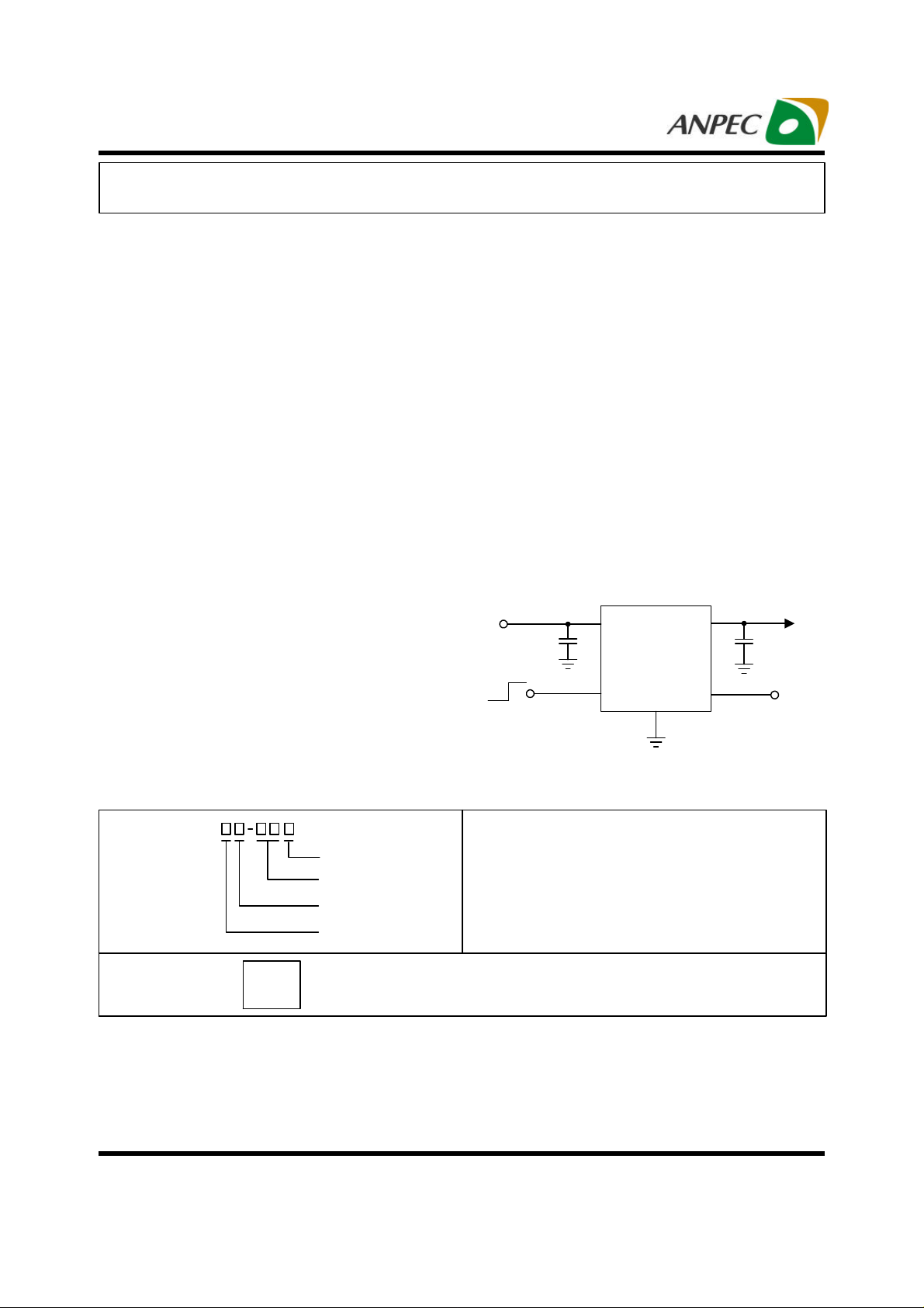
Simplified Application Circuit
V
C2
2.2µF
V
OUT
SET
OFF
V
IN
C1
1µF
ON
VIN
APL5605
EN
GND
VOUT
VSET
Ordering and Marking Information
APL5605
Lead Free Code
Handling Code
Temperature Range
Package Code
APL5605 K :
Note: ANPEC lead-free products contain molding compounds/die attach materials and 100% matte tin plate termination finish; which are fully
compliant with RoHS and compatible with both SnPb and lead-free soldering operations. ANPEC lead-free products meet or exceed the leadfree requirements of IPC/JEDEC J STD-020C for MSL classification at lead-free peak reflow temperature.
ANPEC reserves the right to make changes to improve reliability or manufacturability without notice, and
advise customers to obtain the latest version of relevant information to verify before placing orders.
Copyright ANPEC Electronics Corp.
Rev. A.1 - Jan., 2008
APL5605
XXXXX
Package Code
K : SOP-8
Operating Ambient Temperature Range
I : -40 to 85 C
Handling Code
TR : Tape & Reel
Lead Free Code
L : Lead Free Device
XXXXX - Date Code
°
www.anpec.com.tw1
APL5605
Pin Configuration
SOP-8 Top View
EN 1
VIN 2
VOUT 3
VSET 4
APL5605
Absolute Maximum Ratings (Note 1)
Symbol Parameter Rating Unit
VIN
VEN EN to GND -0.3 ~ VIN+0.3 V
V
VOUT to GND -0.3 ~ VIN+0.3 V
OUT
T
J
PD Power Dissipation Internally Limited
T
STG
T
SDR
Note 1: Stresses beyond the absolute maximum rating may damage the device and exposure to absolute maximum rating conditions for extended
periods may affect device reliability.
VIN to GND
Maximum Junction Temperature
Storage Temperature Range
Maximum Lead Temperature (Soldering, 10 sec)
8 GND
7 GND
6 GND
5 GND
-0.3 ~ 6.5 V
150
-65 ~ 150
260
o
o
o
C
C
C
Thermal Characteristics
Symbol Parameter Rating Unit
Note 2:
θ
JA
θ
is measured with the component mounted on a high effective thermal conductivity test board in free air.
JA
Junction to Ambient Thermal Resistance
SOP-8
80
Recommended Operating Conditions
Symbol Parameter Range Unit
VIN VIN to GND 4.5 ~ 6 V
VEN EN to GND 0 ~ VIN V
V
VOUT to GND 0 ~ VIN-V
OUT
V
VSET to GND 0 ~ 3.3 V
SET
I
Output Current 0 ~ 0.6 A
OUT
CIN Input Capacitor 0.82 ~ 470
C
Output Capacitor 1 ~ 330
OUT
TJ Junction Temperature -40 ~ 125
TA Ambient Temperature -40 ~ 85
V
DROP
°
C/W
µ
°C
°C
F
Copyright ANPEC Electronics Corp.
www.anpec.com.tw2
Rev. A.1 - Jan., 2008
APL5605
Electrical Characteristics
Refer to the typical application circuit. VIN = 5V, VEN = VIN, I
unless otherwise specified. Typical values are at TA = 25 °C.
OUT
= 1mA~600mA, TJ = -40 to 125 °C, TA = -40 to 85°C
,
Symbol
Parameter Test Conditions Min Typ Max Unit
SUPPLY CURRENT
IQ Quiescent Current
VEN = 0V - - 1
VEN = 5V, I
= 0A - 140 200
OUT
UNDER-VOLTAGE-LOCKOUT (UVLO)
VIN UVLO Threshold VIN rising 2.1 2.5 2.9 V
VIN UVLO Hysteresis - 0.15 - V
OUTPUT VOLTAGE
VOUT Voltage / VSET Voltage
VOUT Voltage / VSET Voltage
VSET pin Current
Load Regulation I
V
DROP
Dropout Voltage
TJ = 25°C, VIN=5.5V, I
V
=3.3V
SET
TJ = 40 ~ 125°C, VIN=5.5V, I
V
=1 ~ 3.3V
SET
V
=5V
SET
= 1mA to 600mA - 60 100 mV
OUT
I
=600mA, V
OUT
I
=600mA, V
OUT
I
=600mA, V
OUT
OUT
OUT
OUT
OUT
=2.5V
=3.3V
=5V
=1mA,
OUT
=1mA,
1.552 1.6 1.648 V/V
1.504 1.6 1.696 V/V
- 0.05 1
- 250 400 mV
- 220 350 mV
- 200 320 mV
PROTECTION AND SOFT-START
Output Current Limit 700 - - mA
Thermal Shutdown Temperature - 150 Thermal Shutdown Hysteresis - 40 Foldback Current Limit
V
OUT
< 0.6V
- 250 - mA
TSS Soft-Start Time - 130 300
VOUT Pull Low Resistance VEN=0V, V
=0.5V - 60 -
OUT
LOGIC INPUT
EN Logic Input-High Level 1.6 - - V
EN Logic Input-Low Level - - 0.4 V
EN Pull-Low Resistance VEN<3V - 2 -
µ
A
µ
A
µ
A
°
C
°
C
µ
s
Ω
MΩ
Copyright ANPEC Electronics Corp.
www.anpec.com.tw3
Rev. A.1 - Jan., 2008
APL5605
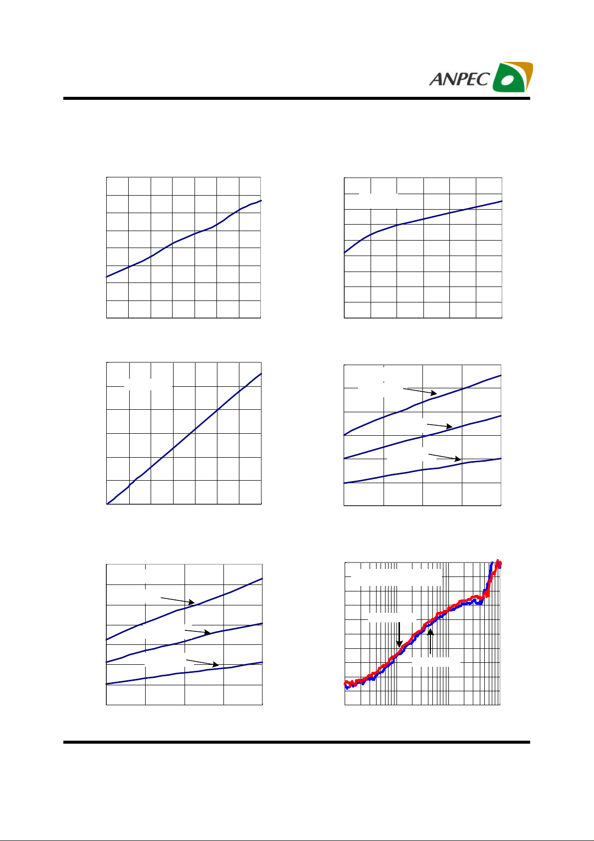
Typical Operating Characteristics
VIN=5V, V
SET
=2V, V
=3.2V, CIN=1µF, C
OUT
=2.2µF, unless otherwise specified.
OUT
EN Voltage threshold vs.
1.6
1.5
1.4
1.3
1.2
1.1
1
EN Voltage Threshold (V)
0.9
0.8
3 3.5 4 4.5 5 5.5 6 6.5
Input Voltage
Input Voltage (V)
VSET Voltage vs. Output Voltage
6
I
5
4
3
OUT
=10mA
Quiescent Current vs. VSET Voltage
180
160
140
(μA)
120
Q
100
Quiescent Current, I
I
=0mA
OUT
80
60
40
20
0
0 0.5 1 1.5 2 2.5 3
VSET Voltage (V)
Dropout vs. Junction Temperature
300
V
=5V
OUT
250
200
150
I
OUT
=600mA
I
OUT
=400mA
2
Output Voltage (V)
1
0
0 0.5 1 1.5 2 2.5 3 3.5
VSET Voltage (V)
Dropout vs. Junction Temperature
350
V
=3.3V
OUT
300
I
=600mA
OUT
250
200
150
100
Dropout Voltage (mV)
50
0
-50 0 50 100 150
I
=400mA
OUT
I
=200mA
OUT
Junction Temperature, T
(°C)
J
I
=200mA
100
Dropout Voltage (mV)
50
0
-50 0 50 100 150
OUT
Junction Temperature, T
J
(°C)
Power Supply Rejection Ratio
=3.2V
OUT
=500mA
OUT
Frequency (Hz)
(PSRR)
=2.2µF,
OUT
I
OUT
=400mA
0
VIN=5, CIN=1µF, C
-5
V
=2V, V
SET
-10
-15
-20
-25
-30
PSRR (dB)
-35
-40
-45
-50
1000 10000 100000 1000000
I
Copyright ANPEC Electronics Corp.
Rev. A.1 - Jan., 2008
www.anpec.com.tw4
APL5605
Typical Operating Characteristics (Cont.)
VIN=5V, V
SET
=2V, V
=3.2V, CIN=1µF, C
OUT
Quiescent Current vs. Input Voltage
200
I
=0mA
OUT
0 1 2 3 4 5 6
Quiescent Current (µA)
160
120
80
40
0
Input Voltage, VIN (V)
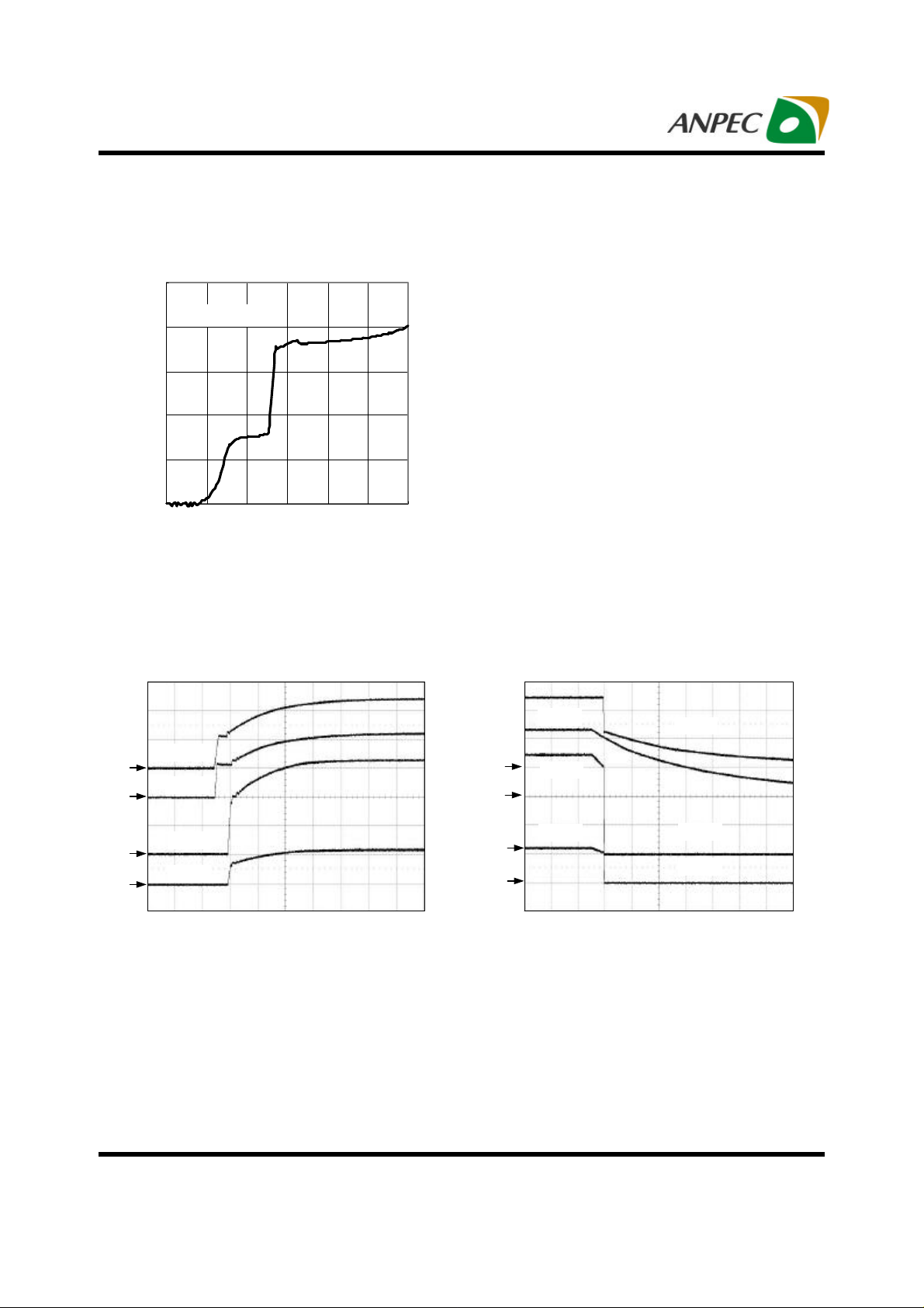
Operating Waveforms
VIN=5V, V
SET
=2V, V
=3.2V, CIN=1µF, C
OUT
Power On
=2.2µF, unless otherwise specified.
OUT
=2.2µF, unless otherwise specified.
OUT
Power Off
1
2
3
4
CH1 : VIN , 2V/div
CH2 : V
CH3 : V
CH4 : I
Time : 1ms/div
V
V
V
I
IN
SET
OUT
OUT
OUT
, 1V/div
SET
, 1V/div
OUT
, 500mA/div
V
SET
1
V
OUT
V
IN
2
I
OUT
V
OUT
3
I
OUT
4
CH1 : VIN , 2V/div
CH2 : V
CH3 : V
CH4 : I
Time : 200ms/div
, 1V/div
SET
, 1V/div
OUT
, 500mA/div
OUT
Copyright ANPEC Electronics Corp.
Rev. A.1 - Jan., 2008
www.anpec.com.tw5

APL5605
Operating Waveforms (Cont.)
VIN=5V, V
SET
=2V, V
=3.2V, CIN=1µF, C
OUT
=2.2µF, unless otherwise specified.
OUT
VIN=5V, V
CIN=1µF, C
1
2
Load transient
=2V , V
SET
=2.2µF
OUT
CH1 : V
CH2 : I
Time : 200µs/div
, 100mV/div
OUT
, 200mV/div
OUT
=3.2V
OUT
Enable
Line transient
VIN=5V, V
CIN=1µF, C
V
OUT
I
OUT
2
1
CH1 : VIN , 1V/div
CH2 : V
Time : 1ms/div
=2V , V
SET
=2.2µF
OUT
, 100mV/div
OUT
OUT
=3.2V
V
IN
V
OUT
Shutdown
V
SET
V
1
EN
2
V
3
4
OUT
I
OUT
CH1 : VEN , 2V/div
CH2 : V
CH3 : V
CH4 : I
Time : 200µs/div
, 1V/div
SET
, 1V/div
OUT
, 500mA/div
OUT
Copyright ANPEC Electronics Corp.
Rev. A.1 - Jan., 2008
1
2
3
4
CH1 : VEN , 2V/div
CH2 : V
CH3 : V
CH4 : I
Time : 10µs/div
, 1V/div
SET
, 1V/div
OUT
, 500mA/div
OUT
V
SET
V
EN
V
OUT
I
OUT
www.anpec.com.tw6

APL5605
Operating Waveforms (Cont.)
VIN=5V, V
SET
=2V, V
=3.2V, CIN=1µF, C
OUT
Thermal Shutdown
=2.2µF, unless otherwise specified.
OUT
Current Limit and Foldback
Current Limit
V
IN
1
V
OUT
V
IN
1
V
2
OUT
2
I
3
CH1 : VIN, 5V/div
CH2 : V
CH3 : I
Time : 500ms/div
, 2V/div
OUT
, 500mA/div
OUT
OUT
3
Time : 2ms/div
CH1 : VIN, 5V/div
CH2 : V
CH3 : I
OUT
OUT
, 2V/div
, 1A/div
I
OUT
Pin Descriptions
Pin
No. Name
1 EN
2 VIN
3 VOUT
Enable Control Input. Driving the EN high turns on the regulator. Pulling the EN low turns the
regulator into shutdown mode. The EN is pulled low by an internal resistor.
Supply Voltage Input Pin. Supply voltage can range from 4.5V to 6V. Bypass with a 1µF (typical)
capacitor to GND
Regulator Output. Sources up to 600mA. A small capacitor is needed from this pin to ground to
assure stability.
4 VSET Output Voltage-Set Input. The output voltage follows the 1.6 times of the VSET voltage.
5,6,7,8 GND
Ground. These pins are internally connected with the internal leadframe. Connect these pins to a
wide ground plane for good heat dissipation.
Function Descriptions
Copyright ANPEC Electronics Corp.
Rev. A.1 - Jan., 2008
www.anpec.com.tw7

APL5605
Block Diagram
VIN
EN
VSET
UVLO and
Soft-Start
Thermal
Shutdown
Current Limit
and Foldback
0.6R
R
V
= V
SET
x 1.6
OUT
VOUT
GND
Typical Application Circuit
V
IN
C
IN
1µF
ON
V
EN
OFF
VIN
EN
APL5605
GND
V1.6 V ⋅=
VSET
VOUT
SETOUT
V
V
C
OUT
2.2µF
SET
OUT
Copyright ANPEC Electronics Corp.
Rev. A.1 - Jan., 2008
www.anpec.com.tw8

APL5605
Function Descriptions
Under-Voltage Lock-Out (UVLO)
The APL5605 has a built-in under-voltage lock-out circuit
to keep the output off until the internal circuitry is operating properly. The UVLO function initiates a soft start process after input voltage exceeds its rising UVLO threshold during power on. Typical UVLO threshold is 2.5V
with 0.15V hysteresis.
Soft-Start
The APL5605 provides an internal soft-start circuitry to
control rise rate of the output voltage and limit the current surge during start-up. Approximate 20µs delay time
after the VIN is over the UVLO threshold, the IC starts a
soft-start. The typical soft-start interval is about 130µs.
Enable/Shutdown
Driving the EN high turns on the regulator, driving the EN
low puts the regulator into shutdown mode. A logic low
also causes the output voltage to discharge to GND. The
EN is pulled low by an internal resistor.
Current Limit
The APL5605 provides a current limit circuitry, which
monitors the output current and controls P-MOS’s gate
voltage to limit the output current at 700mA.
Thermal Shutdown
A thermal shutdown circuit limits the junction temperature
of APL5605. When the junction temperature exceeds
+150οC, the thermal shutdown circuitry disables the
output, allowing the device to cool down. The output
circuitry is enabled again after the junction temperature cools down by 40οC, resulting in a pulsed output
during continuous thermal overload conditions.
Foldback Current Limit
When the output voltage drops below 0.6V (typical),which
is caused by over load or short circuit, the foldback current limit circuitry limits the output current to 250mA. The
foldback current limit is used to ruduce the power dissipation during short circuit condition. The foldback current
limits is disabled for 0.8ms(typical) after UVLO threshold
is reached, so that the IC has normal 700mA (typical)
current limit level during start-up.
Copyright ANPEC Electronics Corp.
Rev. A.1 - Jan., 2008
www.anpec.com.tw9

APL5605
Application Information
Input Capacitor
The APL5605 requires proper input capacitors to supply
surge current during stepping load transients to prevent
the input rail from dropping. Because the parasitic inductor from the voltage sources or other bulk capacitors to
the VIN limits the slew rate of the surge current, place the
Input capacitors near VIN as close as possible. Input
capacitors should be larger than 0.82µF.
Output Capacitor
The APL5605 needs a proper output capacitor to maintain circuit stability and to improve transient response
over temperature and current. In order to insure the circuit stability, the proper output capacitor value should be
larger than 1µF. With X5R and X7R dielectrics, 2.2µF is
sufficient at all operating temperatures. Maximum output
capacitor should be less than 330µF to insure the system can be powered on effectively.
Operation Region and Power Dissipation
The APL5605 maximum power dissipation depends on
the thermal resistance and temperature difference between the die junction and ambient air. The power dissipation PD across the device is:
AJ
)TT(
−
D
P
=
JA
θ
where (TJ-TA) is the temperature difference between the
junction and ambient air. θJA is the thermal resistance
between Junction and ambient air. Assuming the TA=25οC
and maximum TJ=150οC (typical thermal limit threshold),
the maximum power dis sipation is calculated as:
P
=(150-25)/80
D(max)
= 1.56(W)
For normal operation, do not exceed the maximum junction temperature rating of TJ = 125οC. The calculated
power dis sipation should less than:
PD =(125-25)/80
= 1.25(W)
The GND provides an electrical connection to ground and
channels heat away. Connect the GND to ground by us ing a large pad or ground plane.
PCB Layout Considerations
Figure 1 illustrates the layout. Below is a checklist for
your layout:
1. Please place the input capacitors close to the VIN
2. Ceramic capacitors for load must be placed near the
load as close as poss ible
3. To place APL5605 and output capacitors near the load
is good for performance.
4. Large current paths, the bold lines in figure 1, must
have wide tracks.
V
IN
C
IN
V
EN
APL5605
VIN
EN
GND
VSET
VOUT
V
SET
V
OUT
C
OUT
Figure 1
Optimum performance can only be achieved when the
device is mounted on a PC board according to the SOP-8
Board Layout diagram.
For dissipating heat
GND
C
GND
OUT
V
OUT
SOP-8
V
IN
C
IN
Figure 2
Recommanded Minimum Footprint
0.024
8 7 6 5
0.072
0.212
1 2 3 4
0.050
Unit : Inch
Copyright ANPEC Electronics Corp.
Rev. A.1 - Jan., 2008
www.anpec.com.tw10

APL5605
Pack age Information
SOP-8
A
A1
A2
b
c
D
E
E1
e
h
L
0
D
SEE VIEW A
E
E1
h X 45
e
A2
A
A1
VIEW A
S
Y
M
B
O
L
MILLIMETERS
MIN. MAX.
SOP-8
1.75
0.10
0.25
1.25
0.31 0.51
0.17 0.25
4.80
5.80
3.80
5.00
6.20
4.00
cb
0.25
GAUGE PLANE
L
INCHES
MIN. MAX.
SEATING PLANE
0.069
0.004
0.010
0.049
0.012 0.020
0.007 0.010
0.189 0.197
0.228 0.244
0.150 0.157
1.27 BSC 0.050 BSC
0.25 0.50
0.40 1.27
0
8
0.010 0.020
0.016 0.050
0
8
Note: 1. Follow JEDEC MS-012 AA.
2. Dimension “D” does not include mold flash, protrusions or gate burrs.
Mold flash, protrusion or gate burrs shall not exceed 6 mil per side.
3. Dimension “E” does not include inter-lead flash or protrusions.
Inter-lead flash and protrusions shall not exceed 10 mil per side.
Copyright ANPEC Electronics Corp.
Rev. A.1 - Jan., 2008
www.anpec.com.tw11

APL5605
Carrier Tape & R eel Dimensions
OD0
B0
P0
P2
P1
A
E1
F
W
A0
SECTION B-B
13.0+0.50
-0.20
1.5+0.10
-0.00
OD1
B
T
1.5 MIN. 20.2 MIN.
1.5 MIN.
0.6+0.00
-0.40
A
d
12.0±0.30 1.75±0.10 5.5±0.05
6.40±0.20 5.20±0.20 2.10±0.20
Application
SOP-8
K0
SECTION A-A
T1
B
A
H
A H T1 C d D W E1 F
330.0±2.00
50 MIN.
12.4+2.00
-0.00
P0 P1 P2 D0 D1 T A0 B0 K0
4.0±0.10 8.0±0.10 2.0±0.05
(mm)
Devices Per Unit
Package Type Unit Quantity
SOP-8 Tape & Reel 2500
Copyright ANPEC Electronics Corp.
Rev. A.1 - Jan., 2008
www.anpec.com.tw12

APL5605
Reflow Condition (IR/Convection or VPR Reflow)
T
P
Ramp-up
T
L
Tsmax
Tsmin
Temperature
ts
Preheat
25
°
t 25 C to Peak
tp
t
L
Ramp-down
Critical Zone
TL to T
Time
Reliability Test Program
Test item Method Description
SOLDERABILITY MIL-STD-883D-2003
HOLT MIL-STD-883D-1005.7
PCT JESD-22-B, A102
TST MIL-STD-883D-1011.9
245°C, 5 sec
1000 Hrs Bias @125°C
168 Hrs, 100%RH, 121°C
-65°C~150°C, 200 Cycles
ESD MIL-STD-883D-3015.7 VHBM > 2KV, VMM > 200V
Latch-Up JESD 78 10ms, 1tr > 100mA
Classification Reflow Profiles
P
Profile Feature Sn-Pb Eutectic Assembly Pb-Free Assembly
Average ramp-up rate
(TL to TP)
Preheat
Temperature Min (Tsmin)
-
- Temperature Max (Tsmax)
- Time (min to max) (ts)
Time maintained above:
- Temperature (TL)
- Time (tL)
3°C/second max. 3°C/second max.
100°C
150°C
60-120 seconds
183°C
60-150 seconds
150°C
200°C
60-180 seconds
217°C
60-150 seconds
Peak/Classification Temperature (Tp) See table 1 See table 2
Time within 5°C of actual
Peak Temperature (tp)
Ramp-down Rate
Time 25°C to Peak Temperature
10-30 seconds 20-40 seconds
6°C/second max. 6°C/second max.
6 minutes max. 8 minutes max.
Note: All temperatures refer to topside of the package. Measured on the body surface.
Copyright ANPEC Electronics Corp.
Rev. A.1 - Jan., 2008
www.anpec.com.tw13

APL5605
Classification Reflow Profiles (Cont.)
Table 1. SnPb Eutectic Process – Package Peak Reflow Temperatures
Package Thickness
<2.5 mm
≥2.5 mm 225 +0/-5°C 225 +0/-5°C
Table 2. Pb-free Process – Package Classification Reflow Temperatures
Volume mm
<350
240 +0/-5°C 225 +0/-5°C
3
Volume mm
≥350
3
Package Thickness
<1.6 mm
1.6 mm – 2.5 mm
≥2.5 mm 250 +0°C* 245 +0°C* 245 +0°C*
* Tolerance: The device manufacturer/supplier shall assure process compatibility up to and including the stated
classification temperature (this means Peak reflow temperature +0°C. For example 260°C+0°C) at the rated MSL
level.
Volume mm3
<350
260 +0°C* 260 +0°C* 260 +0°C*
260 +0°C* 250 +0°C* 245 +0°C*
Volume mm3
350-2000
Volume mm3
>2000
Customer Service
Anpec Electronics Corp.
Head Office :
No.6, Dusing 1st Road, SBIP,
Hsin-Chu, Taiwan, R.O.C.
Tel : 886-3-5642000
Fax : 886-3-5642050
Taipei Branch :
2F, No. 11, Lane 218, Sec 2 Jhongsing Rd.,
Sindian City, Taipei County 23146, Taiwan
Tel : 886-2-2910-3838
Fax : 886-2-2917-3838
Copyright ANPEC Electronics Corp.
Rev. A.1 - Jan., 2008
www.anpec.com.tw14

 Loading...