ANALOG DEVICES UG-406 Service Manual
Evaluation Board User Guide
UG-406
10676-001
One Technology Way • P.O. Box 9106 • Norwood, MA 02062-9106, U.S.A. • Tel: 781.329.4700 • Fax: 781.461.3113 • www.analog.com
Evaluation Board for the ADF4150HV PLL Frequency Synthesizer
FEATURES
General-purpose evaluation board for ADF4150HV,
including octave range VCO, loop filter and TCXO
Contains the ADF4150HV frequency synthesizer (500 MHz to
3 GHz)
Contains the ADF5001 prescaler to allow optional
connection of external microwave VCOs without need for
an active loop filter
Accompanying software allows complete control of
synthesizer functions from a PC
EVALUATION KIT CONTENTS
EVAL-ADF4150HVEB1Z board
CD that includes
Self-installing software that allows users to control the
board and exercise all functions of the device
Electronic version of the ADF4150HV data sheet
Electronic version of the UG-406 user guide
ADDITIONAL EQUIPMENT
PC running Windows XP or more recent version
Power supply
Spectrum analyzer
Oscilloscope (optional)
DOCUMENTS NEEDED
ADF4150HV data sheet
REQUIRED SOFTWARE
Analog Devices ADF4150HV software (Version 2 or higher)
ADIsimPLL
GENERAL DESCRIPTION
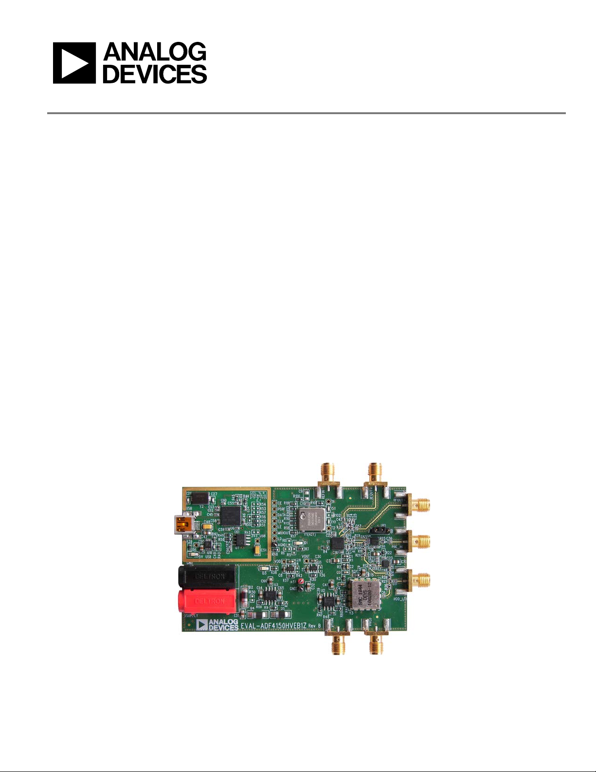
This board is designed to allow the user to evaluate the
performance of the ADF4150HV frequency synthesizer for
phase-locked loops (PLLs). Figure 1 shows the board, which
contains the ADF4150HV synthesizer, loop filter, voltage
control oscillator (VCO) of 1 GHz to 2 GHz octave range and
up to 28 V high tuning voltage, reference oscillator (TCXO)
of 25 MHz frequency for the reference input, power supply
connectors, and an RF output. The ADF5001 prescaler allows
for optional direct connection of external microwave VCOs
without the need for an active loop filter.
The evaluation kit also contains software that is compatible with
Windows® XP and later versions to allow easy programming of
the synthesizer.
A USB port in the PC is required to program the part.
PLEASE SEE THE LAST PAGE FOR AN IMPORTANT
WARNING AND LEGAL TERMS AND CONDITIONS.
EVALUATION BOARD
Figure 1. EVAL-ADF4150HVEB1Z
Rev. 0 | Page 1 of 24

UG-406 Evaluation Board User Guide
TABLE OF CONTENTS
Features .............................................................................................. 1
Evaluation Kit Contents ................................................................... 1
Additional Equipment ..................................................................... 1
Documents Needed .......................................................................... 1
Required Software ........................................................................ 1
General Description ......................................................................... 1
Evaluation Board .............................................................................. 1
Revision History ............................................................................... 2
Quick Start Guide ............................................................................. 3
Evaluation Board Hardware ............................................................ 4
Power Supplies .............................................................................. 4
Input Signals .................................................................................. 4
REVISION HISTORY
5/12—Revision 0: Initial Version
Output Signals ...............................................................................4
Default Operation Settings ..........................................................4
Additional Options .......................................................................5
Phase Noise Measurement ...........................................................5
Evaluation Board Setup Procedure .................................................6
Software Installation .....................................................................6
Evaluation Board Software ...............................................................9
Evaluation and Test ........................................................................ 13
Evaluation Board Schematics and Artwork ................................ 14
Bill of Materials ............................................................................... 22
Related Links ................................................................................... 23
Rev. 0 | Page 2 of 24

Evaluation Board User Guide UG-406
QUICK START GUIDE
Follow these steps to quickly evaluate the ADF4150HV device:
1. Install the ADF4150HV software.
2. Connect the E VA L-ADF4150HVEB1Z board to the PC.
3. Follow the hardware driver installation procedure.
4. Connect the power supplies as follows:
a. 30 V to banana connectors
b. 5 V to the test point labeled +5V on the board
5. Run the ADF4150HV software.
6. Connect the spectrum analyzer to the SMA connector,
VCO_I/O.
7. Measure the results.
Rev. 0 | Page 3 of 24
UG-406 Evaluation Board User Guide
10676-002
EVALUATION BOARD HARDWARE
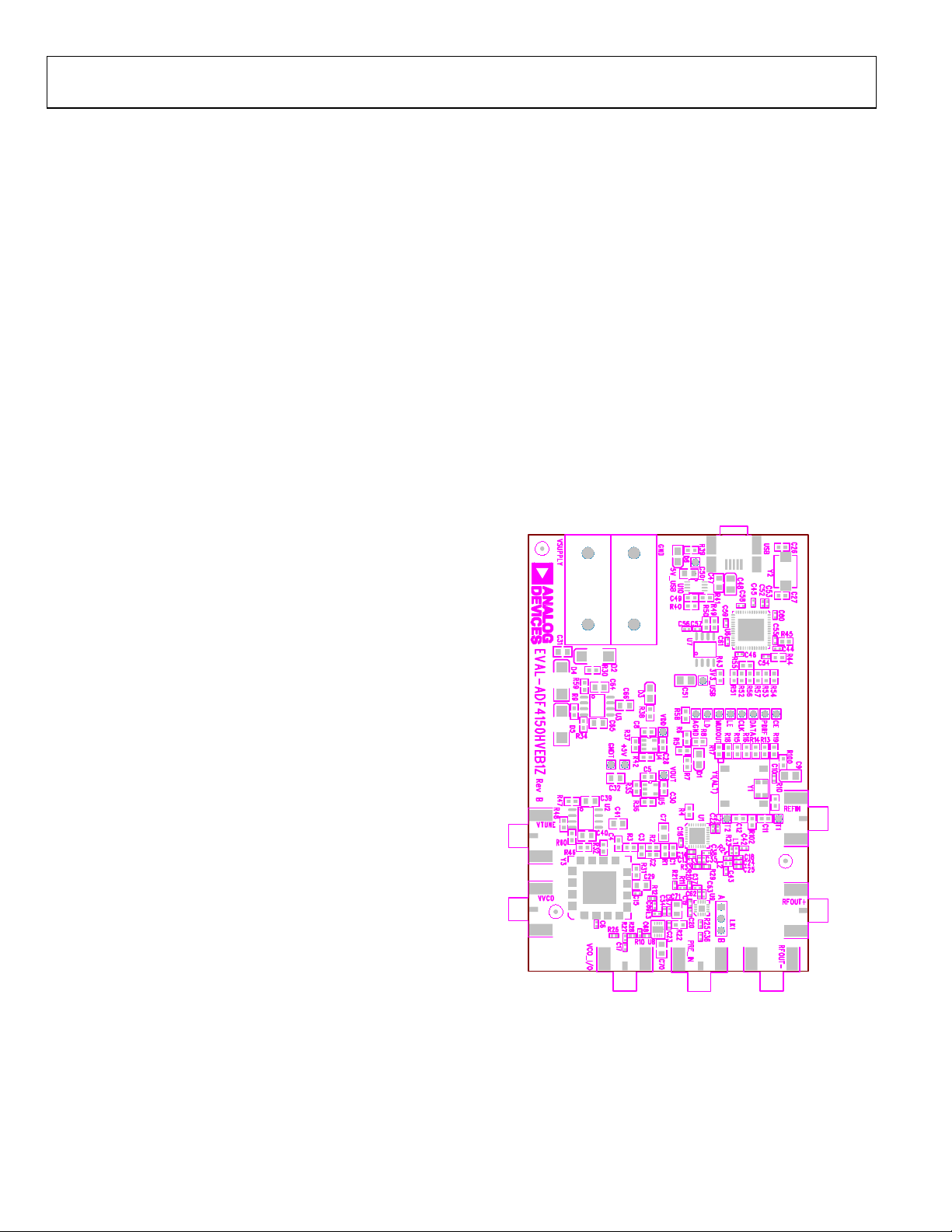
The EVA L -ADF4150HVEB1Z schematics are shown in Figure 25,
Figure 26, Figure 27, and Figure 28. The silkscreen of the
evaluation board is shown in Figure 2.
POWER SUPPLIES
There are two separate supply voltages required for the
evaluation board.
• Banana connectors should be supplied with 30 V. This
powers the LM317LDG regulator, which provides a
regulated 29 V to V
ADF4150HV) and 12 V for the DCYS100200-12 VCO
supply (V
VCO
• The test point labeled +5V must be supplied with 5 V, as
shown in Figure 24. This powers high precision, low noise
ADP150AUJZ-3.3 linear regulators to provide 3.3 V to V
on the board (which supplies the ADF4150HV AV
and SDV
pins), to V
DD
outputs pull-up), and to the ADL5541 buffer, which
improves PFD spur levels at the VCO output.
The D3 LED indicates when the ADF4150HV is powered.
(the charge pump supply of the
P
).
(supply for the ADF4150HV RF
OUT
, DVDD ,
DD
DD
from the VCO ouput, the ADL5541 is not needed and can be
bypassed.
The device is quite sensitive to impedance unbalance. If only
one port of the differential pair is used, the other should be
terminated with a 50 Ω load. The external VCO output should
also be terminated in a 50 Ω load.
DEFAULT OPERATION SETTINGS
This board is shipped with a TCXO that provides a reference
frequency of 25 MHz, a fourth-order low-pass filter with 20 kHz
bandwidth at I
1 GHz to 2 GHz frequency range. To t es t the performance of
the part for a different frequency range and different loop filter,
the relevant components on the board must be changed.
Note that the Synergy VCO tuning sensitivity decreases as the
tuning voltage increases (see Figure 3). To maintain a constant
loop filter bandwidth, increase the charge pump value to the
maximum of 400 µA for frequencies greater than approximately
1.8 GHz.
= 300 μA, and an octave range VCO with a
CP
INPUT SIGNALS
The reference signal is necessary for proper operation of the
synthesizer. It can be sourced from a provided TCXO or from
an external generator, which can be connected to the REFIN
edge mount connector. To u s e an external reference generator, it
is necessary to remove R101 and R100 to disconnect the TCXO
from the reference input and from the supply. R102 can be populated with a 50 Ω resistor to adjust the impedance matching of
the evaluation board to the external reference source.
Digital SPI signals are supplied from the Cypress microcontroller, U6, which is used for communication with the USB port
of the PC.
OUTPUT SIGNALS
All components necessary for LO generation are inserted on the
board. The PLL is made up of the ADF4150HV synthesizer, a
fourth-order passive loop filter, and the octave range VCO. The
loop filter is inserted between the charge pump output and the
VCO input, as shown in Figure 28. If replacing the VCO, a VCO
in a T-package (or similar) must be used. The VCO output is
available at the edge mount SMA connector, VCO_I/O, and the
differential RF output of the part is connected to the RFOUT+
and RFOUT− edge mount SMA connectors.
A buffer, the ADL5541, is placed between the VCO output and
the ADF4150HV RF
spur levels seen at the VCO output below −110 dBc. If the PFD
spur level measured on the VCO output without a buffer is
sufficient (approximately −80 dBc) or if the output signal is
taken only from the RF output pins of the ADF4150HV and not
+ pin, which significantly lowers the PFD
IN
Figure 2. Evaluation Board Silkscreen
Rev. 0 | Page 4 of 24
Evaluation Board User Guide UG-406
VTUNE (V)
kV (MHz/V)
70
65
60
50
55
40
45
30
35
20
25
10
15
0 2 4 6 8 10 12 14 16 18 20 22 24 26 28
10676-003
10676-004
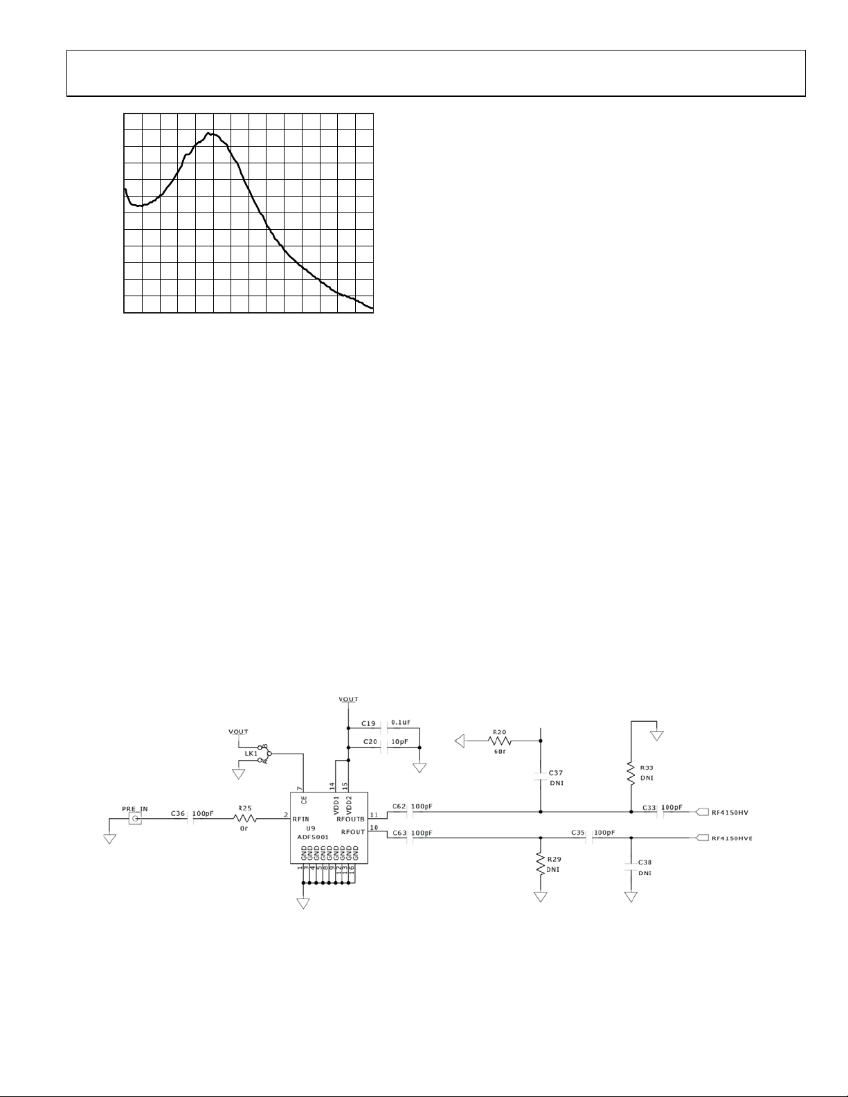
Prescaler for Microwave VCO
The board contains the ADF5001, an 18 GHz divide-by-4
prescaler for users who want to interface a high frequency
microwave VCO to the ADF4150HV. For example, using a
12 GHz external VCO, use the VTUNE SMA as described in
the External VCO Option section, but, in this case, connect the
VCO output to the PRE_IN SMA connector. The prescaler
must be enabled by moving Jumper LK1 into Position B. The
ADF4150HV should be programmed to accept a 12 GHz ÷ 4
frequency, or 3 GHz. Isolate the VCO tracks from the output of
the prescaler by removing C37. It is recommended to interface
the prescaler differentially for best performance; therefore, swap
C38 (100 pF) into the space provided for C35. R33 can be
Figure 3. Frequency Gain vs. Tuning Voltage for DCYS100200-12 VCO
ADDITIONAL OPTIONS
The VVCO connector can be used as a test point to measure the
supply voltage of the VCO in its default configuration. It can
also be used to provide an external supply for the on-board
VCO; however, if an external supply for VCO is used, Resistor R31
must be removed to disconnect the connector from the output
of the on-board voltage regulator.
External VCO Option
Optionally, an external VCO can be used. In this case, it is
necessary to remove R32 and insert a 0 Ω link at R46 to form a
connection between the loop filter output and the VTUNE
SMA edge mount connector. Remove R31 to disconnect the onboard VCO from the power supply. Remove Resistor R26 to
disconnect the output of the on-board VCO from the RF signal
path, and replace Resistors R27 and R28 with 0 Ω links to
ensure operation of the VCO_I/O connector as an input from
an external VCO.
removed as shown in Figure 4. Note the loop filter should be
redesigned when changing the VCO and/or reference
frequencies.
PHASE NOISE MEASUREMENT
With the default settings, in-band phase noise of close to
−101 dBc/Hz can be measured. This translates to a normalized
phase noise floor of −211 dBc/Hz. To measure the ADF4150HV
normalized phase noise specification of −213 dBc/Hz, increase
the loop bandwidth to 50 kHz or greater. The simplest way to
do this is to change the RSET resistor (R4) to 3.3 kΩ. This
increases the charge pump current from 400 µA to 618 µA
with a corresponding increase in loop bandwidth. With the
wider loop bandwidth, a phase noise of −103 dBc/Hz can be
measured:
PN = −213 + 10log(25 MHz) + 20log(1500/25) =
−103 dBc/Hz
The variation of phase noise vs. PLL loop bandwidth can be
modeled in ADIsimPLL.
Figure 4. Configuration of the Board for External Microwave VCO Using the ADF5001 Prescaler
Rev. 0 | Page 5 of 24
UG-406 Evaluation Board User Guide
10676-005
10676-006
10676-007
10676-008
EVALUATION BOARD SETUP PROCEDURE
SOFTWARE INSTALLATION
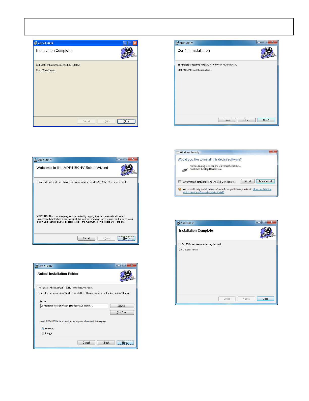
Use the following steps to install the software.
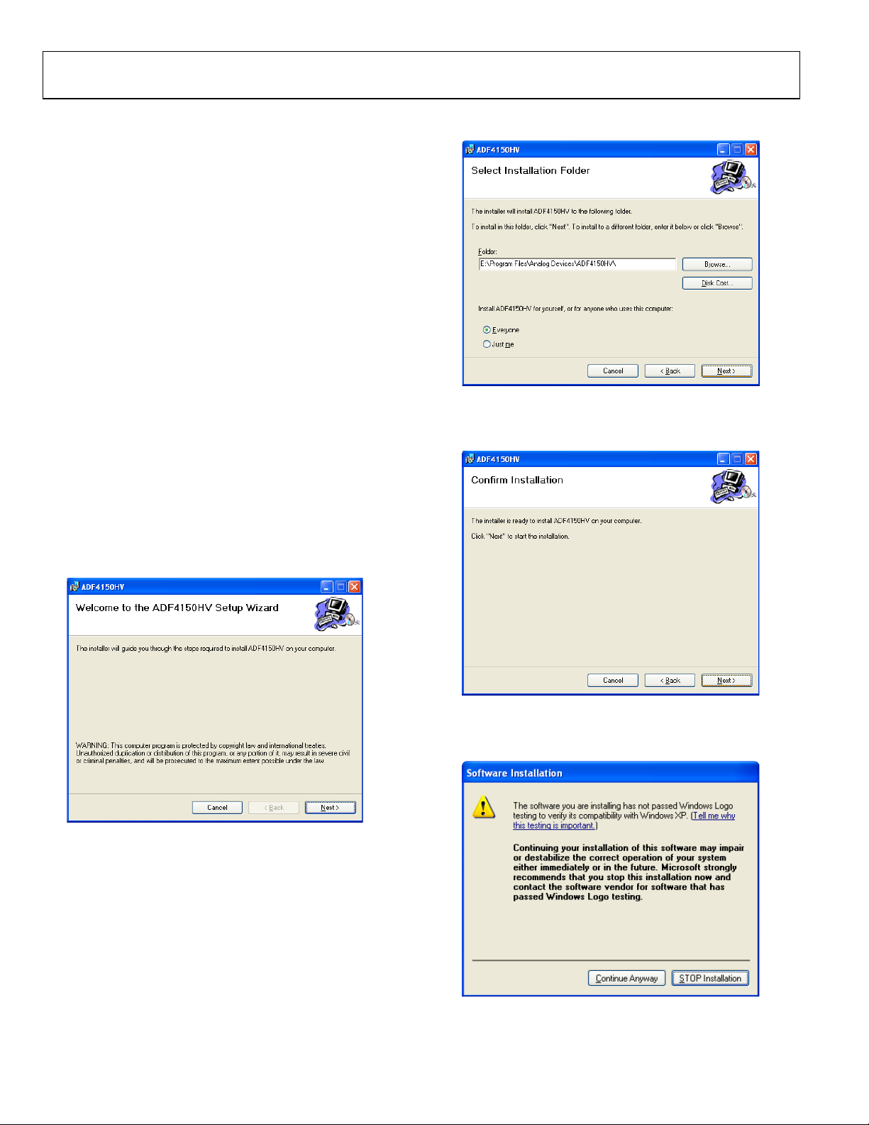
1. Install the Analog Devices ADF4150HV software by
double-clicking ADF4150HV Setup.msi.
If you are using Windows XP, follow the instructions in the
Windows XP Software Installation Guide section (see
Figure 5 to Figure 9).
If you are using Windows Vista or Windows 7, follow the
instructions in the Windows Vista and Windows 7 Software
Installation Guide section (see Figure 10 to Figure 14).
Note that the software requires Microsoft Windows
Installer and Microsoft .NET Framework 3.5 (or higher).
The installer connects to the Internet and downloads
Microsoft .NET Framework automatically. Alternatively,
before running the ADF4150HV Setup.msi, both the
installer and .NET Framework can be installed from the
CD provided.
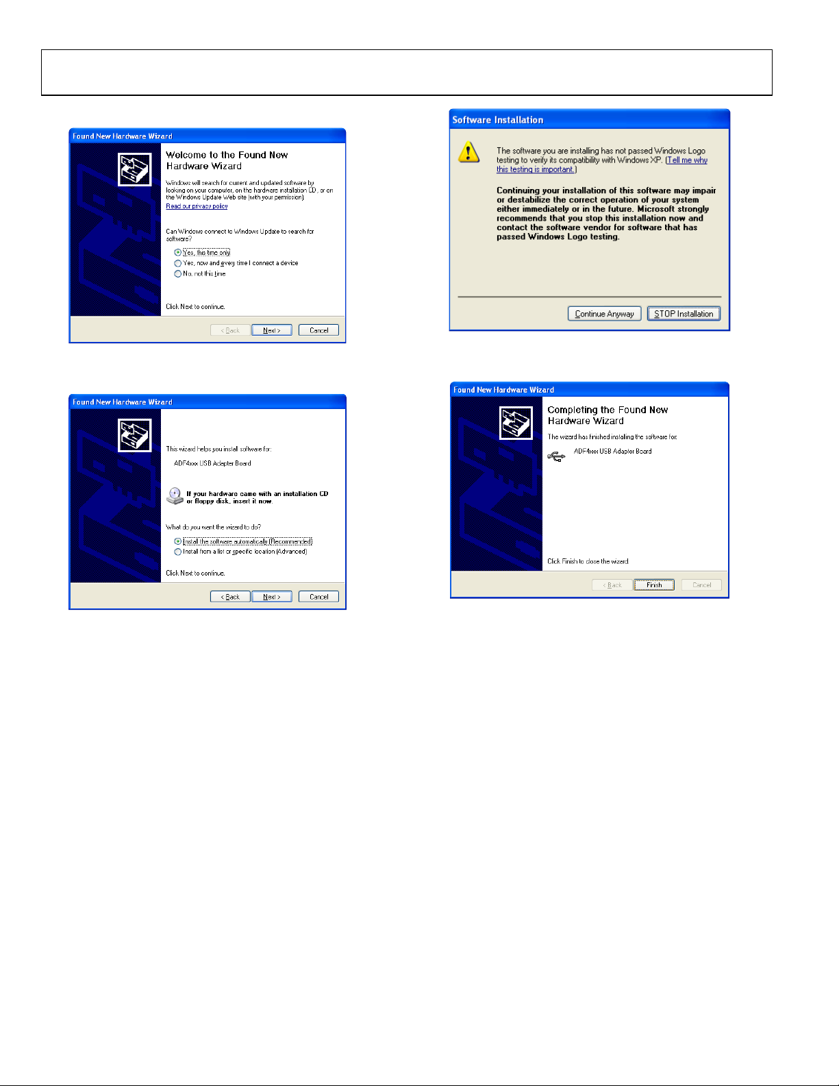
2. Connect your board by USB.
If you are using Windows XP, follow the steps in the
Windows XP Driver Installation Guide section (see Figure 15
to Figure 18).
On Windows Vista or Windows 7, the drivers install
automatically.
Figure 6. Windows XP ADF4150HV Software Installation, Select Installation
Folder
2. Choose an installation directory and click Next.
Windows XP Software Installation Guide
Figure 5. Windows XP ADF4150HV Software Installation, Setup Wizard
1. Click Next.
Figure 7. Windows XP ADF4150HV Software Installation, Confirm
Installation
3. Click Next.
Figure 8. Windows XP ADF4150HV Software Installation, Logo Testing
4. Click Continue Anyway.
Rev. 0 | Page 6 of 24
Evaluation Board User Guide UG-406
10676-009
10676-010
10676-011
10676-012
10676-013
10676-014
Figure 9. Windows XP ADF4150HV Software Installation, Installation
Complete
5. Click Close.
Windows Vista and Windows 7 Software Installation Guide
Figure 10. Windows Vista/7 ADF4150HV Software Installation, Setup Wizard
1. Click Next.
Figure 12. Windows Vista/7 ADF4150HV Software Installation, Confirm
Installation
3. Click Next.
Figure 13. Windows Vista/7 ADF4150HV Software Installation, Start
Installation
4. Click Install.
Figure 11. Windows Vista/7 ADF4150HV Software Installation, Select
Installation Folder
2. Choose an installation directory and click Next.
Figure 14. Windows Vista/7 ADF4150HV Software Installation,
Installation Complete
5. Click Close.
Rev. 0 | Page 7 of 24
UG-406 Evaluation Board User Guide
10676-015
10676-016
10676-017
10676-018
Windows XP Driver Installation Guide
Figure 15. Windows XP USB Driver Installation, Found New Hardware Wizard
1. Choose Ye s, this time only and click Next.
Figure 16. Windows XP USB Driver Installation, Install Options
2. Click Next.
Note that Figure 16 may list Analog Devices RFG.L Eval Board
instead of ADF4xxx USB Adapter Board.
Figure 17. Windows XP USB Driver Installation, Logo Testing
3. Click Continue Anyway.
Figure 18. Windows XP USB Driver Installation, Complete Installation
4. Click Finish.
Rev. 0 | Page 8 of 24
 Loading...