Evaluation Board User Guide
UG-322
10199-001
One Technology Way • P.O. Box 9106 • Norwood, MA 02062-9106, U.S.A. • Tel: 781.329.4700 • Fax: 781.461.3113 • www.analog.com
Evaluation Board for the AD5110 Digital Potentiometer
FEATURES
Full-featured evaluation board for the AD5110
Several test circuits
Various ac/dc input signals
PC control via a separately purchased system demonstration
platform (SDP)
PC control software
Resistor tolerance error stored in EEMEM
PACKAGE CONTENTS
EVAL-AD511xSDZ evaluation board
CD that includes
Self-installing software that allows users to control the
board and exercise all functions of the device
Electronic version of the AD5110 data sheet
Electronic version of the UG-322 user guide
GENERAL DESCRIPTION
This user guide describes the evaluation board for evaluating the
AD5110—a single-channel, 128-position, nonvolatile memory
digital potentiometer.
The AD5110 supports single-supply 2.3 V to 5.5 V operation,
making the device suited for battery-powered applications and
many other applications, offering guaranteed low resistor
tolerance errors of ±8% and high bandwidth while allowing
up to ±6 mA current density in the A, B, and W pins.
The logic voltage levels operate from single 1.8 V to 5.5 V
supplies.
The versatile I
of the wiper register and EEPROM content which contain the
resistor tolerance, providing an end-to-end tolerance accuracy
of 0.1%.
The EVA L -AD5110SDZ can operate in single-supply mode and
incorporates an internal power supply from the USB.
Complete specifications for the AD5110 part can be found in
the AD5110 data sheet, which is available from Analog Devices,
Inc., and should be consulted in conjunction with this user
guide when using the evaluation board.
2
C-compatible digital interface allows readback
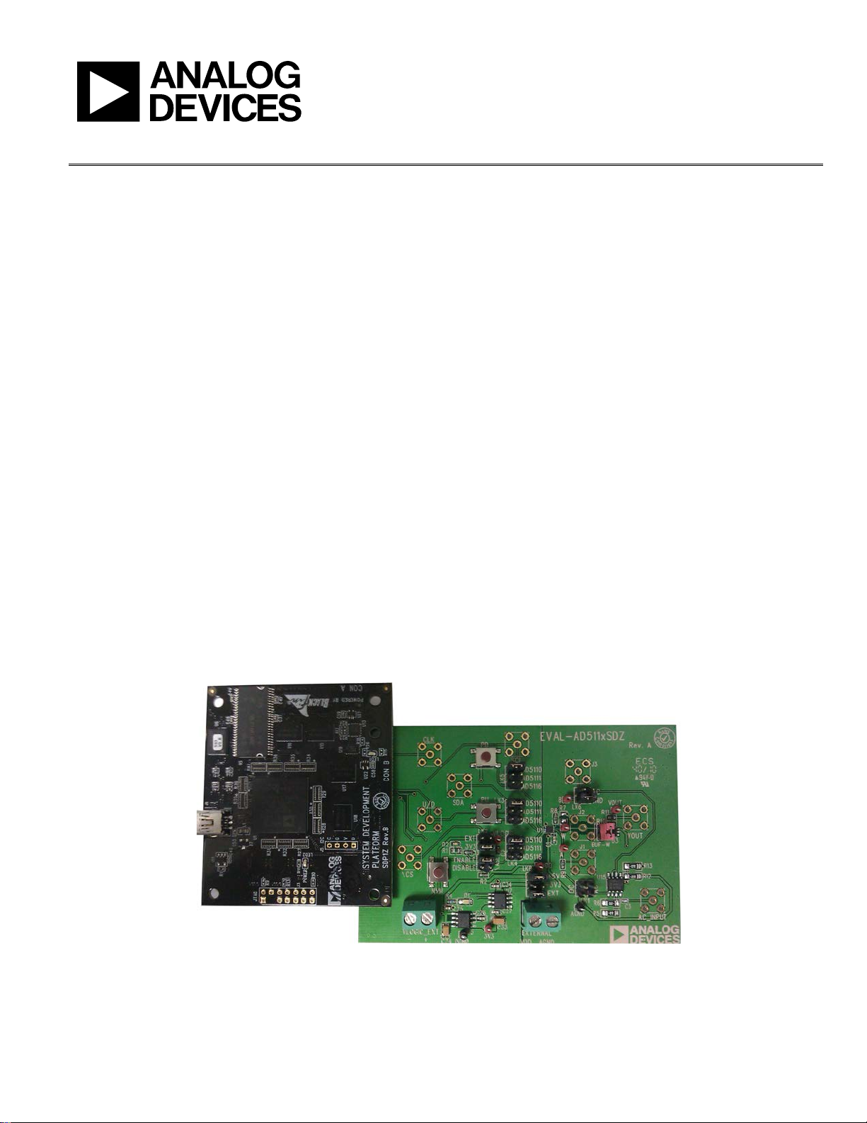
DIGITAL PICTURE OF EVALUATION BOARD WITH SYSTEM DEMONSTRATION PLATFORM
PLEASE SEE THE LAST PAGE FOR AN IMPORTANT
WARNING AND LEGAL TERMS AND CONDITIONS.
Figure 1.
Rev. 0 | Page 1 of 12

UG-322 Evaluation Board User Guide
TABLE OF CONTENTS
Features .............................................................................................. 1
Package Contents .............................................................................. 1
General Description ......................................................................... 1
Digital Picture of Evaluation Board with System
Demonstration Platform.................................................................. 1
Revision History ............................................................................... 2
Evaluation Board Hardware ............................................................ 3
Power Supplies .............................................................................. 3
Link Options ................................................................................. 3
REVISION HISTORY
11/11—Revision 0: Initial Version
Test Circuits ...................................................................................4
Evaluation Board Software ...............................................................5
Installing the Software ..................................................................5
Running the Software ...................................................................5
Software Operation .......................................................................6
Evaluation Board Schematics and Artwork ...................................7
Ordering Information .................................................................... 11
Bill of Materials ........................................................................... 11
Rev. 0 | Page 2 of 12

Evaluation Board User Guide UG-322
EVALUATION BOARD HARDWARE
POWER SUPPLIES
The E VA L-AD5110SDZ supports using single power supplies.
The evaluation board can be powered either from the SDP
port or externally by the EXTERNAL-1 and EXTERNAL-2
connectors, as described in Ta ble 2.
The digital logic levels can be powered either from the SDP
port or externally by the VLOGIC_EXT-1 and VLOGIC_EXT-2
connectors, as described in Tabl e 2.
All supplies are decoupled to ground using 10 µF tantalum and
0.1 µF ceramic capacitors.
Table 2. Maximum and Minimum Voltages of the Connectors
Connector Number Label Voltage
EXTERNAL-1 VDD Analog positive power supply, VDD.
If connected to the SDP, VDD is 3.3 V to 5.5 V.
If controlled externally, VDD is 2.3 V to 5.5 V.
EXTERNAL-2 AGND Analog ground, AGND.
VLOGIC_EXT-1 VLOGIC_EXT + Logic positive power supply, V
If connected to the SDP board, V
If controlled externally, V
VLOGIC_EXT-2 VLOGIC_EXT − Logic ground, DGND.
LINK OPTIONS
Several link and switch options are incorporated in the evaluation board and should be set up before using the board. Tabl e 1
describes the positions of the links to control the evaluation board
by a PC, via the SDP board, using the E VA L-AD5110SDZ. The
functions of these link and switch options are described in
detail in Tabl e 3.
Table 1. Link Options Setup for SDP Control (Default)
Link No. Option
LK2 3V3
LK8 +5V
.
LOGIC
is 3.3 V.
LOGI C
is 1.8 V to VDD.
LOGIC
Table 3. Link Functions
Link Number Power Supply Option
LK2 V
3V3 (from SDP).
EXT (external supply from the VLOGIC_EXT connector).
LK8 VDD This link selects one of the following as the positive power supply:
+5V (from SDP).
+3V3 (from SDP).
EXT1 (external supply from the EXTERNAL connector).
1
If the part is powered using the external connector without connecting the SDP board, +5V jumper must be connected as well.
This link selects one of the following as the logic power supply:
LOGIC
Rev. 0 | Page 3 of 12

UG-322 Evaluation Board User Guide
VOUT
V
DD
AC
DC
GND
A
B
W
BUF-W
+
–
W
AC
V
DD
2
V
DD
2
B
A
750Ω
12Ω
R9
R8
10199-002
256
)(
RDAC
VVV
B
A
OUT
×−=
B
A
AC
AC
GND
A
B
W
BUF-W
AC_INPUT
W
VOUT
+
–
V
DD
2
V
DD
2
HPF
f
C
= 200Hz
12Ω
750Ω
R8
R9
R7
10199-003
×≈
128
log20)dB(
RDAC
nAttenuatio
TEST CIRCUITS
The E VA L-AD5110SDZ incorporates several test circuits to
evaluate the AD5110 performance.
DAC
The AD5110 can be operated as a digital-to-analog converter
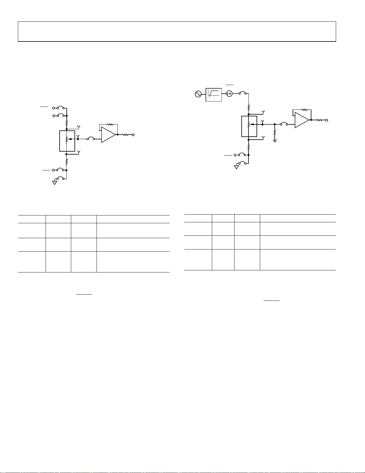
(DAC), as shown in Figure 2.
AC Signal Attenuation
The AD5110 can be used to attenuate an ac signal, which must
be provided externally using the AC_INPUT connector, as
shown in Figure 3.
Figure 2. DAC
Tabl e 4 shows the options available for the voltage references.
Table 4. DAC Voltage References
Termi nal Link Options Description
A LK1 AC Connects Terminal A to VDD/2
DC Connects Terminal A to VDD
W BUF-W Connects Terminal W to an
output buffer
B LK6 AC Connects Terminal B to VDD/2
GND Connects Terminal B to
analog ground
The output voltage is defined in Equation 1.
(1)
where:
RDAC is the code loaded in the RDAC register.
V
is the voltage applied to Terminal A (LK1 link).
A
V
is the voltage applied to Terminal B (LK6 link).
B
However, by using the R8 and R9 external resistors, the user can
reduce the voltage of the voltage references. In this case, use the
A and B test points to measure the voltage applied to the A and
B terminals and recalculate V
and VB in Equation 1.
A
Figure 3. AC Signal Attenuator
Depending on the voltage supply rails and the dc offset voltage
of the ac signal, various configurations can be used as described
in Tabl e 5.
Table 5. AC Signal Attenuation Link Options
Termi nal Link Options Description
A LK1 AC Remove dc voltage and biased
the signal to V
/2
DD
W BUF-W Connects Terminal W to an
output buffer
B LK6 AC1 Connects Terminal B to VDD/2
GND Connects Terminal B to analog
ground
1
Recommended to ensure optimal total harmonic distortion (THD) performance.
The signal attenuation is defined in Equation 2.
(2)
where:
RDAC is the code loaded in the RDAC register.
In addition, R7 can be used to achieve an exponential attenuation. To do so, adjust the R7 resistor until a desirable transfer
function is found, typically around 1.6 kΩ for a 10 kΩ
potentiometer.
Rev. 0 | Page 4 of 12
 Loading...