ANALOG DEVICES UG-282 Service Manual

SDP Breakout Board User Guide
One Technology Way • P. O . Box 9106 • Norwood, MA 02062-9106, U.S.A. • Tel : 781.329.4700 • Fax : 781.461.3113 • www.analog.com
UG-282
SDP Breakout Board User Guide
INTRODUCTION
This user guide is written for system engineers who use the
system demonstration platform (SDP); it discusses how to use
the SDP breakout board when designing SDP-compatible
hardware and software.
The ADZS-BRKOUT-EX3 SDP breakout board from Analog
Devices, Inc., can be used in conjunction with SDP controller
boards and daughter boards designed on the SDP system. The
breakout board allows signals travelling between SDP controller
boards and compatible daughter boards to be monitored by the
insertion of the breakout board between the SDP controller
board and the daughter board.
SDP controller boards are used as part of the evaluation system
for many Analog Devices components. The SDP breakout
board exposes each of the 120 pins of the SDP controller board's
connector allowing users to monitor signals between the
controlling board and the attached daughter evaluation board
or Circuit from the Lab™ reference circuit board.
This user guide describes the SDP breakout board (ADZS-
BRKOUT-EX3). The Getting Started section provides
information on how to use the SDP breakout board as a debug
tool for the SDP 120-pin connector signals. The Hardware
Description section describes the ADZS-BRKOUT-EX3
hardware. This includes details of the connectors on the board
and how these signals are exposed. The ADZS-BRKOUT-EX3
schematics are provided in the Schematic section.
PLEASE SEE THE LAST PAGE FOR AN IMPORTANT
WARNING AND LEGAL TERMS AND CONDITIONS.
Rev. 0 | Page 1 of 16

UG-282 SDP Breakout Board User Guide
TABLE OF CONTENTS
Introduction ...................................................................................... 1
Revision History ............................................................................... 2
Product Overview............................................................................. 3
Technical or Customer Support.................................................. 3
Product Information.................................................................... 3
Regulatory Compliance ............................................................... 3
Getting Started .................................................................................. 4
Package Contents.......................................................................... 4
REVISION HISTORY
9/11—Revision 0: Initial Version
PC Configuration..........................................................................4
Breakout Board Installation.........................................................4
Hardware Description.......................................................................5
LEDs................................................................................................5
Through-Hole Probe Points.........................................................5
Connector Pin Assignments........................................................6
Schematics....................................................................................... 10
Rev. 0 | Page 2 of 16

SDP Breakout Board User Guide UG-282
PRODUCT OVERVIEW
The SDP breakout board features
• 4-pin × 120-pin small footprint connectors
• Hirose FX8-120P-SV1(91),120-pin header
• Hirose FX8-120S-SV(21), 120-pin receptacle
• ID EEPROM
• 240 through-hole probe points
For more information, go to http://www.analog.com/sdp.
TECHNICAL OR CUSTOMER SUPPORT
You can reach Analog Devices, Inc., Customer Support in the
following ways:
• Visit the SDP website at
http://www.analog.com/sdp
• Email processor questions to
processor.support@analog.com (worldwide support)
processor.europe@analog.com (Europe support)
processor.china@analog.com (China support)
• Phone questions to
1-800-ANALOGD
• Contact your Analog Devices local sales office or
authorized distributor.
• Send questions by mail to:
Analog Devices, Inc.
Three Technology Way
P.O. Box 9106
Norwood, MA 02062-9106
USA
PRODUCT INFORMATION
Product information can be obtained from the Analog Devices
website.
Analog Devices Website
The Analog Devices website, http://www.analog.com, provides
information about a broad range of products—analog
integrated circuits, amplifiers, converters, and digital signal
processors.
Note that MyAnalog.com is a free feature of the Analog Devices
website that allows customization of a web page to display
only the latest information about products of interest to you.
You can choose to receive weekly email notifications containing
updates to the web pages that meet your interests, including
documentation errata. MyAnalog.com provides access to books,
application notes, data sheets, code examples, and more.
Visit MyAnalog.com to sign up. If you are a registered user, just
log on. Your user name is your email address.
REGULATORY COMPLIANCE
The ADZS-BRKOUT-EX3 is designed for use solely in a
laboratory environment. The board is not intended for use as
a consumer end product or as a portion of a consumer end
product. The board is an open system design, which does
not include a shielded enclosure and therefore may cause
interference to other electrical devices in close proximity. This
board should not be used in or near any medical equipment or
RF devices. Store unused boards in the protective shipping
package.
The ADZS-BRKOUT-EX3board has been certified to comply
with the essential requirements of the European EMC directive
89/36/EC, amended by 93/68/EEC, and therefore carries the
CE mark.
Rev. 0 | Page 3 of 16

UG-282 SDP Breakout Board User Guide
GETTING STARTED
This section provides specific information to assist you with
using the SDP breakout board as part of an SDP system.
The following topics are covered.
• Package contents
• PC configuration
• Breakout board installation
PACKAGE CONTENTS
The ADZS-BRKOUT-EX3 board package contains one
ADZS-BRKOUT-EX3 board.
Contact the vendor where you purchased the SDP breakout
board or contact Analog Devices if this item is missing.
PC CONFIGURATION
For correct operation of an SDP controller board and SDP
breakout board, your computer must have the following
minimum configuration:
• Windows XP Service Pack 2 or Windows Vista®
• USB 2.0 port
BREAKOUT BOARD INSTALLATION
When removing the SDP breakout board from the package,
handle the board carefully to avoid the discharge of static
electricity, which can damage some components.
The SDP breakout board is designed for use with an SDP
controller board. The SDP breakout board must be connected
to a PC via the SDP controller board and a USB cable.
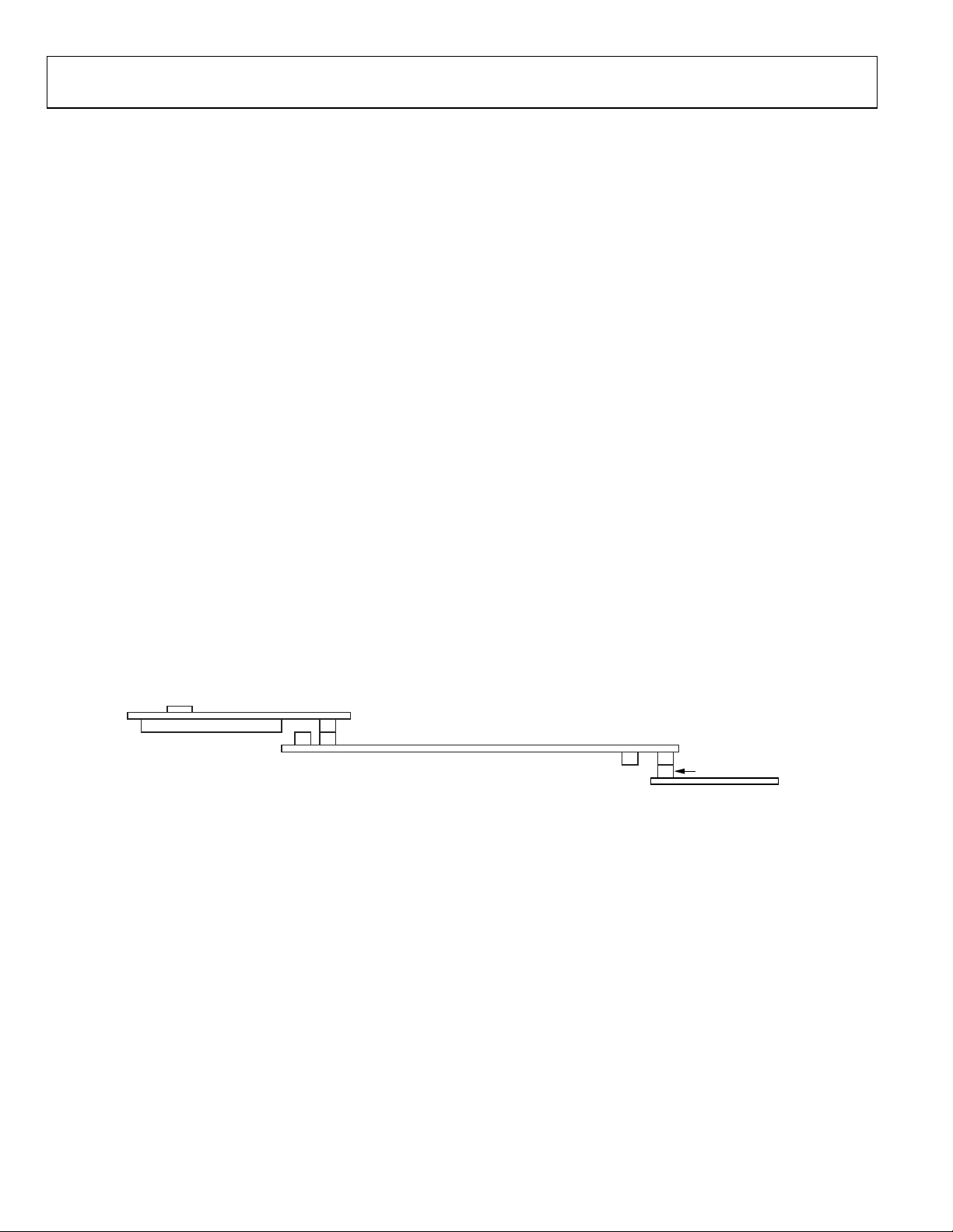
Figure 1 shows the SDP breakout board connected to an
SDP-B controller board and a Circuit from the Lab reference
circuit or component evaluation board.
The SDP breakout board exposes each of the 120 pins on the
SDP-B board connector. The breakout board has a 120-pin
receptacle connector (J1) which attaches to the 120-pin
connector on the SDP controller board; it also has a 120-pin
header connector (P1) for attaching SDP-compatible daughter
boards to the system.
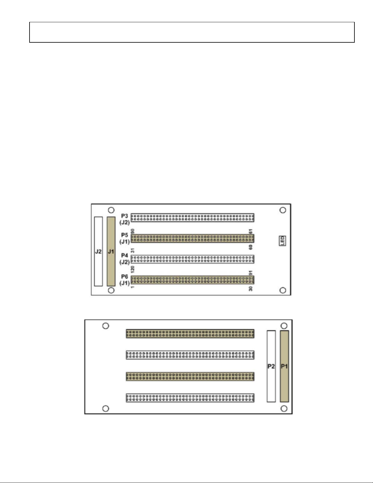
Pin 1 to Pin 30 and Pin 91 to Pin 120 from receptacle J1
are exposed in the P6 set of probe points. Pin 31 to Pin 90
are exposed in the P5 set of probe points. In this way, the
SDP breakout board can be used to monitor signals travelling between the SDP controller board and the attached
daughter board.
The SDP breakout board can also be used as a proof of concept
tool through the insertion of pin headers in the exposed,
relevant signal through-hole locations. These pin headers can
be connected to existing hardware when building up a mock-up
system prior to the design of SDP-specific hardware.
CON B
SDP BOARD
A
J1
J2
SDP-B CONTROLLER BOARD
Figure 1. Connecting the SDP Breakout Board
P2 P1
COMPONE NT E V AL / CftL
CON
DAUGHTER BOARD
09896-001
Rev. 0 | Page 4 of 16

SDP Breakout Board User Guide UG-282
HARDWARE DESCRIPTION
This section describes the hardware design of the ADZS-
BRKOUT-EX3 board.
The following topics are covered.
• LEDs—This section describes the SDP breakout board
LEDs.
• Through-hole probe points—This section provides layouts
of through-hole probe points on the SDP breakout board.
• Connector Pin Assignments—This section details the pin
assignments on the 120-pin connectors.
LEDS
There is a single LED located on the SDP breakout board. It
is connected to the input power line on the 120-pin header
connector on the SDP breakout board. Therefore, when power
is provided from an attached daughter board, this LED is on. If
there is no power coming through the VIN pin on P1, this LED
remains off.
THROUGH-HOLE PROBE POINTS
The SDP breakout board contains 240 through-hole probe
points, 2 × 120 pin receptacle connector and 2 × 120 pin header
connectors. One of the 120-pin receptacle connectors (J1)
can be used to connect to the 120-pin connector on the SDP
controller board. One of the 120-pin header connectors (P1), on
the back of the SDP board, can be used to connect to a daughter
board (P1).
Figure 2 and Figure 3 show both sides of the SDP breakout
board; the shading indicates the signal path from the receptacle
to the header via the through-hole probe points. Connector J2
and P2 are for use with future Blackfin® EZ-Kit products.
The signal lines between these two connectors are exposed
through the probe points on P3 and P4.
09896-002
Figure 2. SDP Breakout Board—Top View
09896-003
Figure 3. SDP Breakout Board—Bottom View
Rev. 0 | Page 5 of 16
 Loading...