Evaluation Board User Guide
UG-250
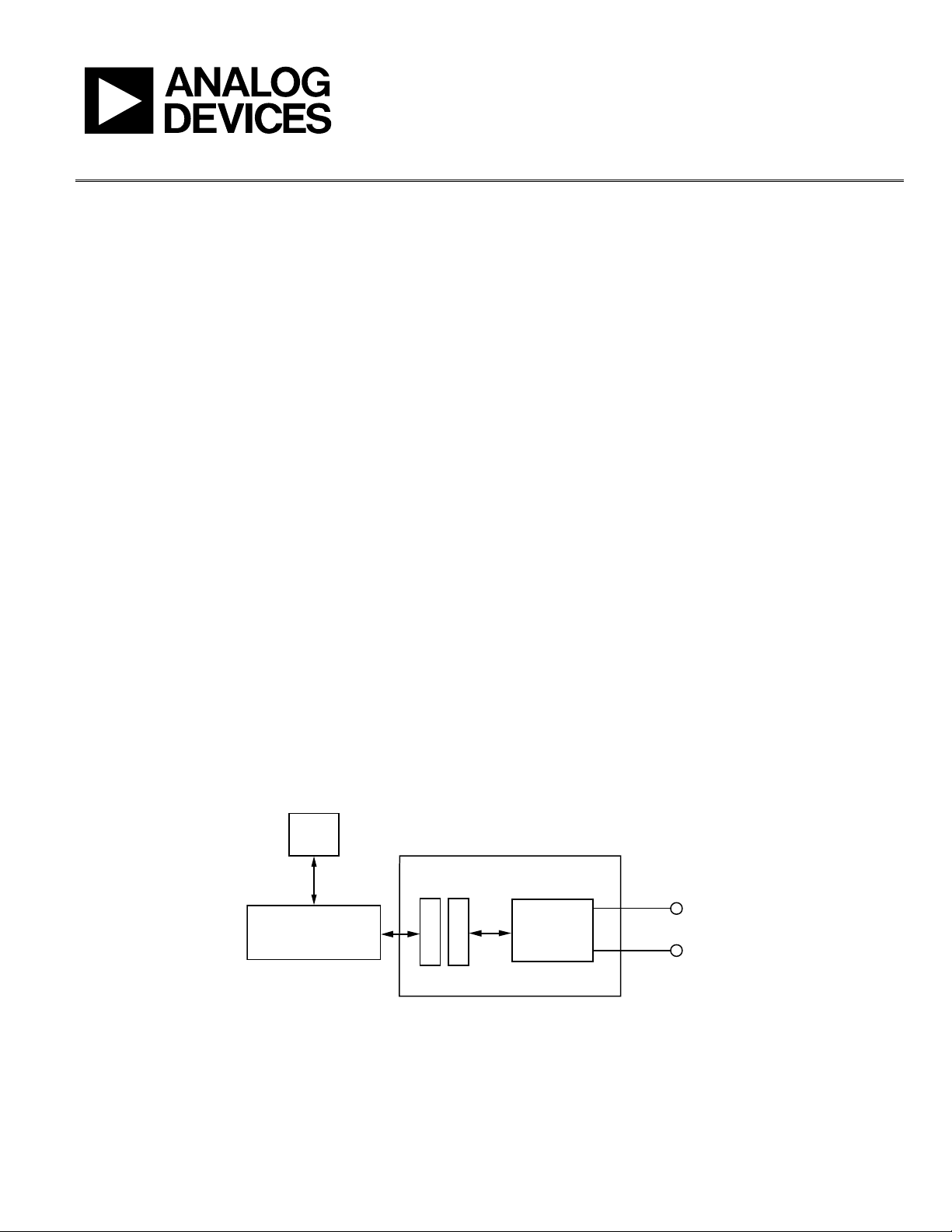
SYSTEM DEMONSTRATION
PLATFORM BOARD
PC
USB
PORT
LOOP+
LOOP–
DIGITAL
ISOLATION
AD5421
EVAL-AD5421SDZ
09701-001
One Technology Way • P.O. Box 9106 • Norwood, MA 02062-9106, U.S.A. • Tel: 781.329.4700 • Fax: 781.461.3113 • www.analog.com
Evaluation Board for 16-Bit, Serial Input, Loop-Powered 4 mA to 20 mA DAC
FEATURES
Full-featured evaluation board for the AD5421
Link options
PC control in conjunction with Analog Devices, Inc.,
system demonstration platform (SDP)
PC software for control
EQUIPMENT NEEDED
DC power supply unit
SDP for PC control (EVAL-SDP-CB1Z)
Voltmeter or ammeter
DOCUMENTS NEEDED
AD5421 data sheet
SOFTWARE NEEDED
AD5421 evaluation software
EVALUATION BOARD DESCRIPTION
The EVAL-AD5421 is a full-featured evaluation board, designed
to allow the user to easily evaluate all features of the AD5421
loop-powered 4 mA to 20 mA DAC. The AD5421 pins are
accessible at on-board connectors for external connection. The
AD5421 evaluation board is controlled via the PC’s USB port in
conjunction with Analog Device’s system demonstration
platform board. The SDP board allows the evaluation board to
be controlled through the USB port of a Windows® XP (SP2 or
later) or Vista-based (32-bit) PC using the AD5421 evaluation
software. The AD5421 serial interface is also accessible at the
testpoint connections on the board.
DEVICE DESCRIPTION
The AD5421 is an integrated device designed for use in looppowered 4 mA to 20 mA smart transmitter applications. The
AD5421, in a single chip, provides a 16-bit DAC and current
amplifier for digital control of the loop current, a voltage
regulator to power the entire transmitter, a voltage reference,
fault alert functions, flexible SPI-compatible serial interface,
gain and offset adjust registers as well as other features and
functions.
Complete specifications for the AD5421 are available in the
AD5421 data sheet available from Analog Devices and should
be consulted in conjunction with this document when using the
evaluation board.
PLEASE SEE THE LAST PAGE FOR AN IMPORTANT
WARNING AND LEGAL TERMS AND CONDITI ONS.
FUNCTIONAL BLOCK DIAGRAM
Figure 1.
Rev. A | Page 1 of 12

UG-250 Evaluation Board User Guide
TABLE OF CONTENTS
Features .............................................................................................. 1
Equipment Needed ........................................................................... 1
Documents Needed .......................................................................... 1
Software Needed ............................................................................... 1
Evaluation Board Description ......................................................... 1
Device Description ........................................................................... 1
Functional Block Diagram .............................................................. 1
Revision History ............................................................................... 2
Evaluation Board Hardware ............................................................ 3
REVISION HISTORY
10/11—Rev. 0 to Rev. A
Change to Figure 4 ........................................................................... 7
3/11—Revision 0: Initial Version
Power Supplies ...............................................................................3
Link Options ..................................................................................3
Evaluation Board Software Quick Start Procedures .....................5
Software Installation .....................................................................5
Software Operation .......................................................................5
Main Window ................................................................................6
Evaluation Board Schematics and Artwork ...................................7
Ordering Information .................................................................... 11
Bill of Materials ........................................................................... 11
Rev. A | Page 2 of 12

Evaluation Board User Guide UG-250
LK7
Inserted
EVALUATION BOARD HARDWARE
POWER SUPPLIES
The AD5421 evaluation board requires one power supply
connection from LOOP− to LOOP+ (J7), a voltage in the
range from 5.5 V to 52 V can be applied if the on-board
MOSFET device (U2) is not enabled. With U2 enabled, the
voltage limit is the breakdown voltage of U2, which in this
case is 240 V. A load resistor can also be connected at J7.
LINK OPTIONS
Set the link options on the evaluation board for the required
operating setup before powering on the board. The functions
of the link options are described in Table 2.
Default Link Option Setup
The default link options are listed in Tabl e 1.
Table 1. Link Options
Link No. Option
LK1 Inserted
LK2 B
LK4 Inserted
LK6 Inserted
Alarm_Dir B
Rint_Rext B
Range0 B
Range1 B
Reg_Sel0 A
Reg_Sel1 B
Reg_Sel2 A
Rev. A | Page 3 of 12

UG-250 Evaluation Board User Guide
B A B
3 V
A B A
9 V
Table 2. Link Options
Link No. Description
LK1 This link connects the V
When this link is inserted, the V
When this link is removed, the V
LK2 This link enables/disables the MOSFET device.
Position A disables the MOSFET device.
Position B enables the MOSFET device and the loop supply is connected directly to the REG
LK4
This link enables/disables the iCoupler® digital isolators.
When this link is inserted, the isolators are enabled.
When this link is removed, the isolators are disabled.
LK6 This link should be inserted when the MOSFET device is enabled (LK2 in Position B).
This link should be removed when the MOSFET device is disabled (LK2 in Position A).
LK7 This link completes the loop connection if a load resistor is not connected at Connector J7.
This link should be inserted if a load resistor is not connected at Connector J7.
This link should be removed if a load resistor is connected at Connector J7.
Alarm_Dir This link selects the alarm current direction.
Position A selects an upscale alarm current (22.8 mA or 24 mA).
Position B selects a downscale alarm current (3.2 mA).
Rint_Rext This link selects to use either the internal or external current setting resistor.
Position A selects the internal resistor.
Position B selects the external resistor.
Range0,
Range1
These links select the loop current range.
Range1 Range0 Loop Range
B B 4 mA to 20 mA
B A 3.8 mA to 21 mA
A B 3.2 mA to 24 mA
A A 3.8 mA to 21 mA
Reg_Sel2,
Reg_Sel1,
Reg_Sel0
These links select the voltage regulator output voltage.
Reg_Sel2 Reg_Sel1 Reg_Sel0 Regulator Output Voltage
B B B 1.8 V
B B A 2.5 V
input pin to the LOOP+ voltage via a 20:1 resistor divider.
LOOP
pin is connected to the resistor divider.
LOOP
pin is unconnected and can be connected to another voltage (maximum 2.5 V) via TP26.
LOOP
pin.
IN
B A A 3.3 V
A B B 5 V
A A B 12 V
Rev. A | Page 4 of 12
 Loading...