Evaluation Board User Guide
One Technology Way • P. O . Box 9106 • Norwood, MA 02062-9106, U.S.A. • Tel : 781.329.4700 • Fax : 781.461.3113 • www.analog.com
UG-176
ADuC7023 Evaluation Board User Guide
MicroConverter ADuC7023 Development System
FEATURES
2-layer printed circuit board (PCB), 4 inch × 5 inch form factor
USB power supply regulated to 3.3 V on board
USB-to-I
20-pin standard JTAG connector for programming/
Demonstration circuit
32.768 kHz watch crystal to drive the PLL clock
ADR291 2.5 V external reference chip
Reset/download/IRQ0 push buttons
Power indicator/general-purpose LEDs
Access to all ADC inputs and DAC outputs from external header;
Surface-mount and through-hole, general-purpose
The full evaluation kit also includes:
2
C programming interface on board
debugging
all device ports are routed to external header pins
prototype area
mIDAS-Link JTAG programming POD
CD containing evaluation software, including user
manuals, data sheets, example code, I2CWSD, and
evaluation compilers
USB cable
GENERAL DESCRIPTION
This user guide refers to the ADuC7023 evaluation boards
provided in the EVAL-ADuC7023QSPZ (32-lead LFCSP device
based) and the EVAL-ADuC7023QSPZ1 (40-lead LFCSP device
based) kits. These evaluation boards allow for the evaluation of
the MicroConverter® ADuC7023. The ADuC7023 contains an
ARM7TDMI core, 64 kB of Flash, 8 kB of SRAM, a 12-bit, 1 MSPS
SAR analog-to-digital converter (ADC), and 4 × 12-bit voltage
digital-to-analog converters (DACs), plus many other features.
These evaluation boards allow users to program the ADuC7023
via the JTAG or the I
source code through the JTAG interface.
In this user guide, all references to the physical orientation of
components on the boards are made with respect to a componentside view of the board with the prototype area appearing in the
bottom of the board.
The boards are laid out to minimize coupling between the analog
and digital sections of the board. To this end, the ground plane
is split with the analog section on the left side and a digital
plane on the right side of the board. The regulated 3.3 V power
supply is routed directly to the digital section and is filtered
before being routed into the analog section of the board.
2
C interfaces. Users may also debug their
PLEASE SEE THE LAST PAGE FOR AN IMPORTANT
WARNING AND LEGAL TERMS AND CONDITIONS.
Rev. 0 | Page 1 of 16

UG-176 Evaluation Board User Guide
TABLE OF CONTENTS
Features .............................................................................................. 1
General Description ......................................................................... 1
Revision History ............................................................................... 2
Evaluation Board Features ............................................................... 3
Power Supply ................................................................................. 3
I2C Programming Interface ......................................................... 3
Emulation Interface ...................................................................... 4
Using P0.4 and P0.5 as I2C Pins .................................................. 4
Crystal Circuit ............................................................................... 4
External Reference (ADR291E) .................................................. 4
Reset/Download/IRQ1 Push-Buttons ....................................... 4
Power Indicator/General-Purpose LEDs .................................. 5
Analog I/O Connections ............................................................. 5
REVISION HISTORY
7/10—Revision 0: Initial Version
General-Purpose Prototype Area ................................................5
DIP Switch Link Options .................................................................6
External Connectors .........................................................................7
Analog I/O Connector, J3 ............................................................7
Emulation Connector, J4 ..............................................................7
Mini-USB Interface Connector, J1 ..............................................7
Digital I/O Connector, J2 .............................................................7
I2C Connector, J9 ...........................................................................7
Evaluation Board, Schematics and Artwork ..................................8
Ordering Information .................................................................... 14
Bill of Materials ........................................................................... 14
Related Links ............................................................................... 15
Rev. 0 | Page 2 of 16

Evaluation Board User Guide UG-176
(
A
3
EVALUATION BOARD FEATURES
POWER SUPPLY
Both boards can be directly powered via the mini-USB connector,
J1. Alternatively, an external 12 V to 5 V power supply can be
connected to the 2-pin header, J7, which is labeled POWER.
The pin beside the mini-USB connector is the power pin.
I2C PROGRAMMING INTERFACE
The ADuC7023 is connected to the USB connector via the
2
C-to-USB transceiver chip referenced as U5 on the PCB. The
I
interface allows direct connection to the PC via the USB port.
Connect the evaluation board to the PC via the USB port using
the mini-USB lead included in the evaluation package.
Prompts appear to install drivers for the new hardware, which
includes the following: Serial Converter A, Serial Converter B, and
the serial ports. The D2XX direct drivers can be found on the
FTDI website. These drivers are also included on the CD with the
evaluation kit.
Complete the following steps to install the drivers for the
FT2232H device on the evaluation board and to download a
hex file to the ADuC7023 internal flash via the I2CWSD
application provided with the evaluation software.
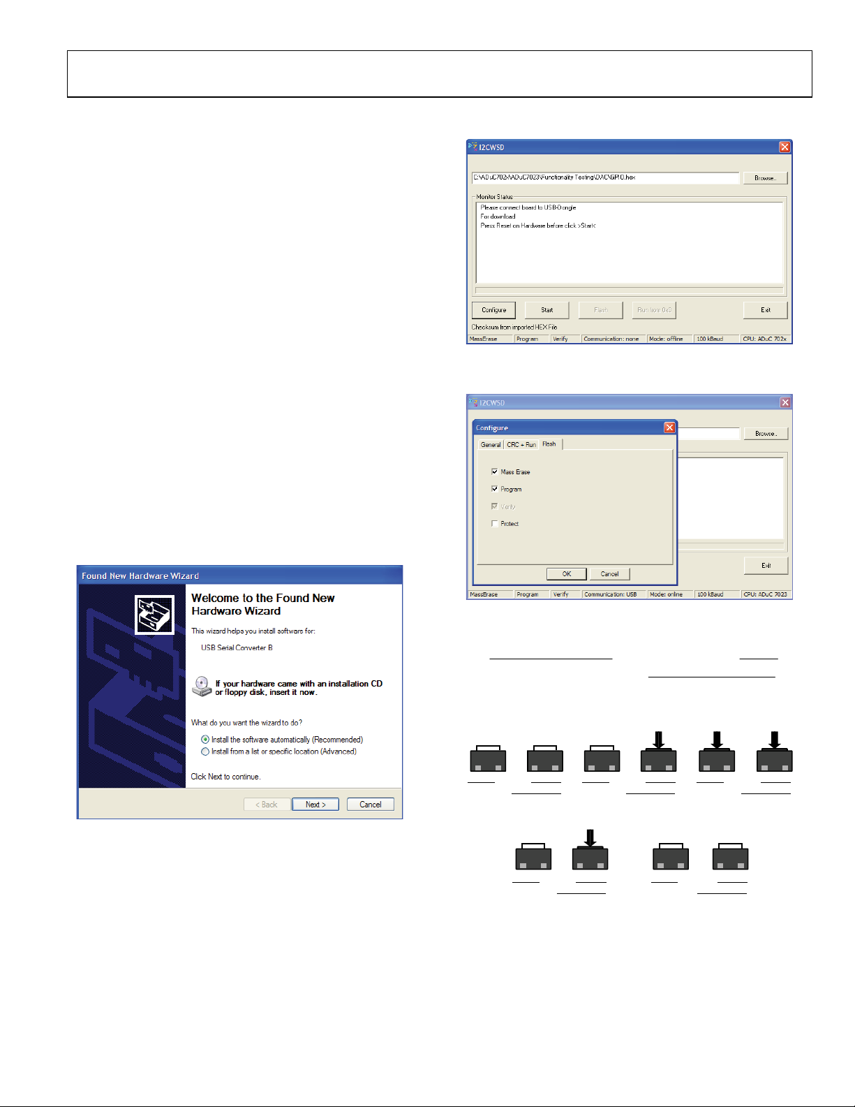
1. Select Install the software automatically (Recommended)
and Click Next > to complete the install (see Figure 1).
3. Click Configure and select the settings shown in Figure 3.
Figure 2. I2CWSD Dialog Box
9195-002
Figure 1. Found New Hardware Wizard Dialog Box
2. To connect to the Microcontroller, open the I2CWSD
application from the Windows® Start menu (see Figure 2).
This may also be downloaded from the ADuC7023 product
page on the Analog Devices, Inc., website. This I2CWSD is
different from the generic I2CWSD application that interfaces
to the USB-I2C/LIN-CONVZ dongle.
09195-003
Figure 3. I2CWSD Configure Options
4. Select the hex files location by clicking Browse.. and reset the
evaluation board. This is done by holding down the
SERIAL DOWNLOAD
button (S2), toggling the
button (S3), and releasing the
SERIAL DOWNLOAD
RESET
switch, which then resets the board (see ). Figure 4
ND S2 RELEASED (B) PUSH S2 (C) PUSH S
(A) S3
S3
RESET = 1)S2(SERIAL
9195-001
DOWNLO AD = 1)
(D) RELEASE S3 (E) RELEASE S2
S3
(RESET = 1)S2(SERIAL
Figure 4. Download Mode Entry Sequence
S3
(RESET = 1)S2(SERIAL
DOWNLOAD = 0)
DOWNLO AD = 0)
S3
(RESET = 1)S2(SERIAL
S3
(RESET = 0)S2(SERIAL
DOWNLO AD = 1)
DOWNLO AD = 0)
09195-004
Rev. 0 | Page 3 of 16

UG-176 Evaluation Board User Guide
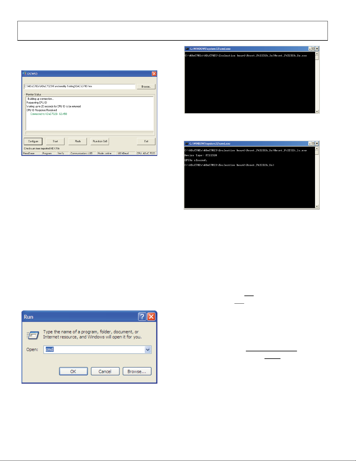
5. Click Start in the I2CWSD dialog box to connect the
I2CWSD download software with the ADuC7023 bootloader
(see Figure 5).
Figure 7. Command to Enter to Run Reset_Ft2232h_Io.exe
Go to the directory where the Reset_Ft2232h_Io.exe utility is
copied on the PC (see Figure 7 and Figure 8).
9195-005
Figure 5. I2CWSD Application Showing a Valid ADuC7023 ID String Response
EMULATION INTERFACE
Nonintrusive emulation and download are possible on the
ADuC7023 via JTAG by connecting a JTAG emulator to the J4
connector.
9195-013
USING P0.4 AND P0.5 AS I2C PINS
The ADuC7023 evaluation boards use an I2C-to-USB transceiver
chip, the FT2232H, that allows the ADuC7023 to be programmed
directly over the USB interface without any need of an external
dongle. However, the FT2232H does drive the P0.4/P0.5 pins of
the ADuC7023 by default. To isolate these pins from the FT2232H,
run the Reset_Ft2232h_Io.exe utility, which can be downloaded
from the ADuC7023 product page on the Analog Devices website.
This utility configures the P0.4/P0.5 connection to the FT2232H as
input pins, which stops the FT2232H from driving these pins.
Execute this utility if the P0.4/P0.5 pins are intended for any use
other than interfacing with the PC via the USB transceiver.
Run the executable from the Command window, as shown in
Figure 6.
Figure 6. How to Open a Command Window
09195-014
Figure 8. Expected Text after Running Reset_Ft2232h_Io.exe
CRYSTAL CIRCUIT
The board is fitted with a 32.768 kHz crystal, from which the
on-chip PLL circuit can generate a 41.78 MHz clock.
EXTERNAL REFERENCE (ADR291E)
The external 2.5 V reference chip, U2, is provided on the
evaluation board to demonstrate the external reference option
of the ADuC7023.
RESET/DOWNLOAD/IRQ1 PUSH-BUTTONS
A reset push button is provided to allow users to reset the part
RST
manually. When pressed, the
to DGND. Because the
RST
pin of the is pulled
pin on the is Schmidttriggered internally, there is no need to use an external Schmidt
trigger on this pin.
When pressed, the IRQ1 push-button switch drives the P1.1 pin
high. This can be used to initiate an External Interrupt 1.
On the evaluation board, serial download mode can be easily
initiated by holding down the
SERIAL DOWNLOAD
(S2) while pressing and releasing the
shown in the section. Also, ensure
2
I
C Programming Interface
that Flash Address 0x80014 contains 0xFFFFFFFF.
09195-012
ADuC7023
ADuC7023
RESET
button (S3), as
push button
Rev. 0 | Page 4 of 16

Evaluation Board User Guide UG-176
POWER INDICATOR/GENERAL-PURPOSE LEDS
A power LED (D5) is used to indicate that a sufficient supply is
available on the board. A general-purpose LED (D2) is directly
connected to VDDIO and connected to P0.7 of the ADuC7023
through R18. When P0.7 is cleared, the LED turns on. When
P0.7 is set, the LED turns off.
ANALOG I/O CONNECTIONS
All analog I/O connections are connected to Header J3.
ADC0 and ADC1 are buffered using an AD8606 to evaluate
single-ended and pseudo differential mode. A potentiometer
can be connected to ADC0 buffered.
ADC3 and ADC2 can be buffered with a single-ended-todifferential op amp on board, with the AD8132 used to
evaluate the ADC in differential mode.
DAC1 can be used to control the brightness of the green LED, D1,
when connected via the S1 switch.
GENERAL-PURPOSE PROTOTYPE AREA
General-purpose prototype areas are provided at the bottom of the
evaluation board for adding external components as required in
the application. As can be seen from the layout, AVDD, AGND,
VDDIO, and DGND tracks are provided in this prototype area
(see the Evaluation Board, Schematics and Artwork section).
Rev. 0 | Page 5 of 16
 Loading...