Evaluation Board User Guide
UG-166
One Technology Way • P. O . Box 9106 • Norwood, MA 02062-9106, U.S.A. • Tel : 781.329.4700 • Fax : 781.461.3113 • www.analog.com
WCDMA Evaluation Board for PLL Frequency Synthesizer
FEATURES
Self-contained board including synthesizer, VCO, and loop
filter for generating WCDMA frequencies (1.93 GHz to
1.99 GHz)
Designed for 20 kHz loop bandwidth
Accompanying software allows complete control of
synthesizer functions from a PC
Battery operated: choice of 3 V or 5 V supplies
Typical phase noise performance of −85 dBc/Hz at 1 kHz
offset
BLOCK DIAGRAM
GENERAL DESCRIPTION
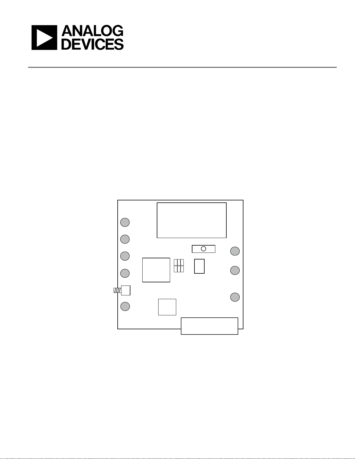
This board is designed to allow the user to evaluate the performance of the ADF4118 frequency synthesizer for phase-locked
loops (PLLs). The block diagram of the board is shown in
Figure 1. It contains the ADF4118 synthesizer, a PC connector,
TCXO for the reference input, SMA connectors for the power
supplies, and an RF output. There is also a low-pass loop filter
(20 kHz) and a VCO (Vari-L VCO190-1960T) on board. A
cable is included with the board to connect to a PC printer port.
The package also contains Windows® software to allow easy
programming of the synthesizer.
FILTER
TCXO
9 VOLT BATTERY
POWER SWITCH
ON OFF
ADF411x
PC CONNECTOR
Figure 1.
V
P
MUXOUT
CE
09156-001
V
DD
V
VCO
TEST
TEST
RF
OUT
REF
IN
SMA
SOCKET
EVAL-ADF411xEBZ1
VCO
PLEASE SEE THE LAST PAGE FOR AN IMPORTANT
WARNING AND LEGAL TERMS AND CONDITIONS.
Rev. 0 | Page 1 of 8

UG-166 Evaluation Board User Guide
TABLE OF CONTENTS
Features.............................................................................................. 1
General Description ......................................................................... 1
Block Diagram .................................................................................. 1
Revision History ............................................................................... 2
REVISION HISTORY
6/11—Revision 0: Initial Version
Evaluation Board Hardware.............................................................3
Loop Components.........................................................................3
Evaluation Board Software...............................................................4
Evaluation Board Schematics...........................................................5
Rev. 0 | Page 2 of 8

Evaluation Board User Guide UG-166
EVALUATION BOARD HARDWARE
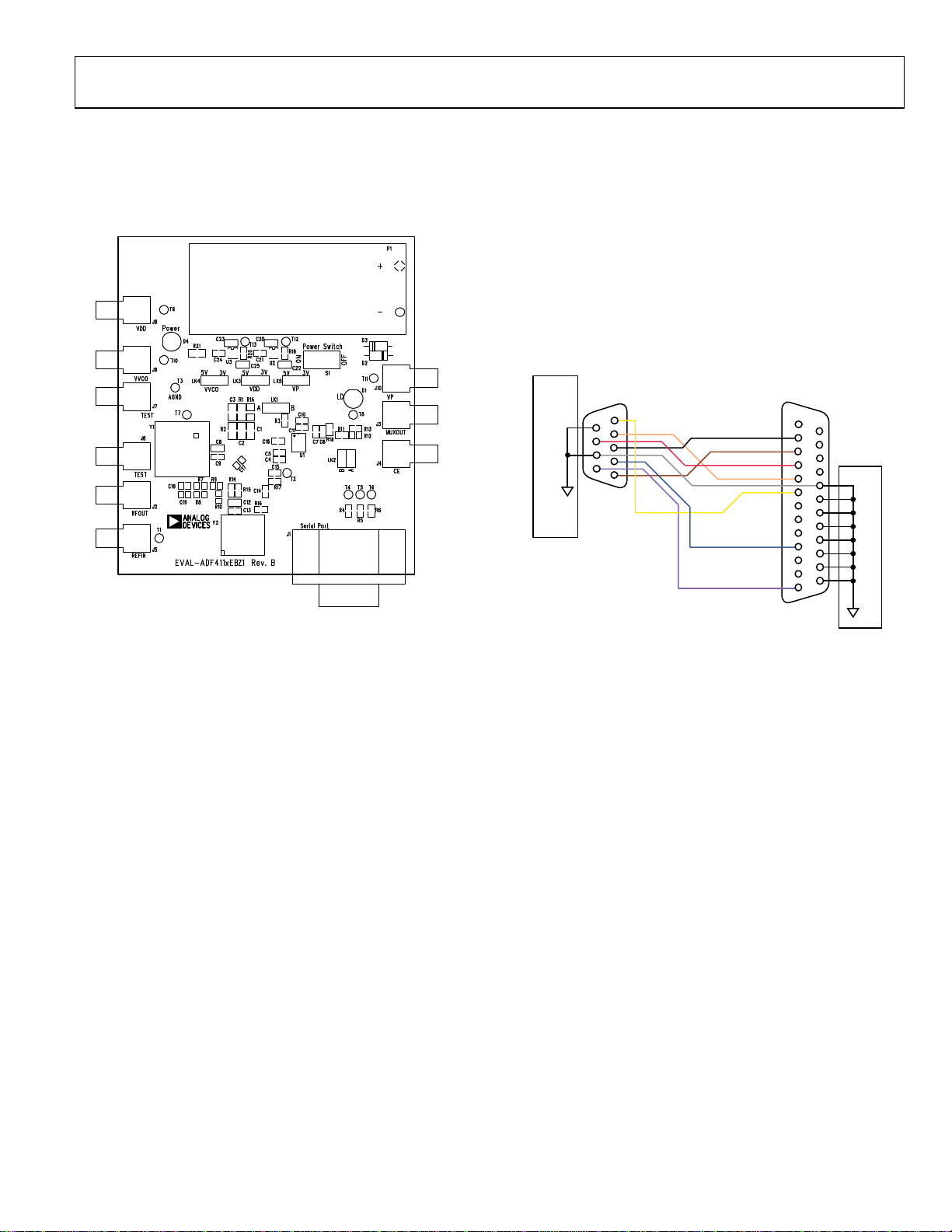
The evaluation board is supplied with a cable for connecting to
the printer port of a PC. The silkscreen and cable diagram for
the evaluation board are shown in Figure 2 and Figure 3, respectively. The board schematics are shown in Figure 5 and Figure 6.
loop filter (20 kHz), and the VCO 190-1960T from Vari-L.
The output is available at RF
through a standard SMA
OUT
connector. Alternatively, users can use their own power supplies
and reference input. In this case, insert SMA connectors as
shown on the silkscreen in Figure 2 and the block diagram in
Figure 1.
LOOP COMPONENTS
C1 = 150 pF, C2 = 1.5 nF, C3 = 82 pF.
R1 = 22 kΩ, R1a = 22 kΩ, R2 = 20 kΩ.
EVAL-ADF411x
EVAL-ADF421x
09156-002
Figure 2. Evaluation Board Silkscreen
The board is powered from a single 9 V battery. The power
supply circuitry allows the user to choose either 3 V or 5 V for
the ADF4118 V
settings are 3 V for the ADF4118 V
V
and for the VCO supply. It is very important to note that the
P
ADF4118 V
and VP and for the VCO supply. The default
DD
and 5 V for the ADF4118
DD
should never exceed the ADF4118 VP. This can
DD
damage the device.
All components necessary for LO generation are included on
board. The 10 MHz TCXO from Vectron provides the necessary
reference input. The PLL is made up of the ADF4118, a passive
1
6
2
7
3
8
4
9
5
9-WAY
FEMALE
D-TYPE
TO
ADF411x
ADF421x
EVALUATION
BOARD
BLACK-CLK
BROWN-DATA
ORANGE-CE
WHITE-GND
YELLOW
PURPLE
1
14
2
15
3
4
5
6
7
8
9
10
11
12
13
25-WAY
MALE
D-TYPE
16
17
18
19
20
21
22
23
24
25
RED-LE
BLUE
TO PC PRINTER PORT
Figure 3. PC Cable Diagram
Loop component values shown in the circuit diagrams (see
Figure 5 and Figure 6) are for a 1.96 GHz RF output, 1 mA
charge pump (CP) current, 200 kHz channel spacing, and
20 kHz loop bandwidth, with a VCO190-1960T.
PC
09156-003
Rev. 0 | Page 3 of 8
 Loading...