

HUSH Stereo Noise Reduction System
13
16
15
14
19
18
17
24
23
22
21
20
12
11
10
9
8
1
2
3
4
7
6
5
L IN
R VCF CAP 2
R VCF CAP 1
R OUT
L OUT
R IN
L VCF CAP 1
L VCF CAP 2
DO NOT CONNECT
1
DIGITAL GND
V–
V+
ANALOG COMMON (V+/2)
VCA CONTROL PORT
VCF DET IN
SUM OUT
VCA DET IN
AUTO
THRESHOLD CAP
DEFEAT
MUTE
VCF DET TC
VCA DET TC
DEFAULT
THRESHOLD
2
1kΩ
2nF
500Ω
20nF
3µF
20nF
1.0µF
3.3µF
6.8µF
6.8µF
1nF
0.22µF
DO NOT CONNECT
1
NOTES:
1
MAKE NO CONNECTION TO PINS 13 AND 18
2
DEFAULT THRESHOLD. NORMALLY CONNECTED TO ANALOG COMMON
1nF
SSM2000
a
FEATURES
Up to 25 dB of Noise Reduction from Virtually Any
Audio Source without Sonic Artifacts
“Single-Ended” Operation Eliminates Need for Encode-
Decode Process
Adaptive Threshold Dynamically Adjusts to Changing
Nominal Signal Levels
Effectively Decodes Dolby B
Direct VCA Control Port Access for Additional Level
Control Functionality
Logic-Controllable Bypass and Muting
100 dB Dynamic Range (Noise Reduction OFF)
0.02% Typical THD+N (@ 1 kHz, Noise Reduction OFF)
+7 V to +18 V Operation
No Royalty Requirements
APPLICATIONS
Auto Radio Sound Processing
Multimedia PC Sound Cards
Television Sound Processing
Cassette Tape Players
AM/FM Receivers
Telephone & Wireless Links
Professional Audio
®
Encoded Sources
with Adaptive Threshold
SSM2000
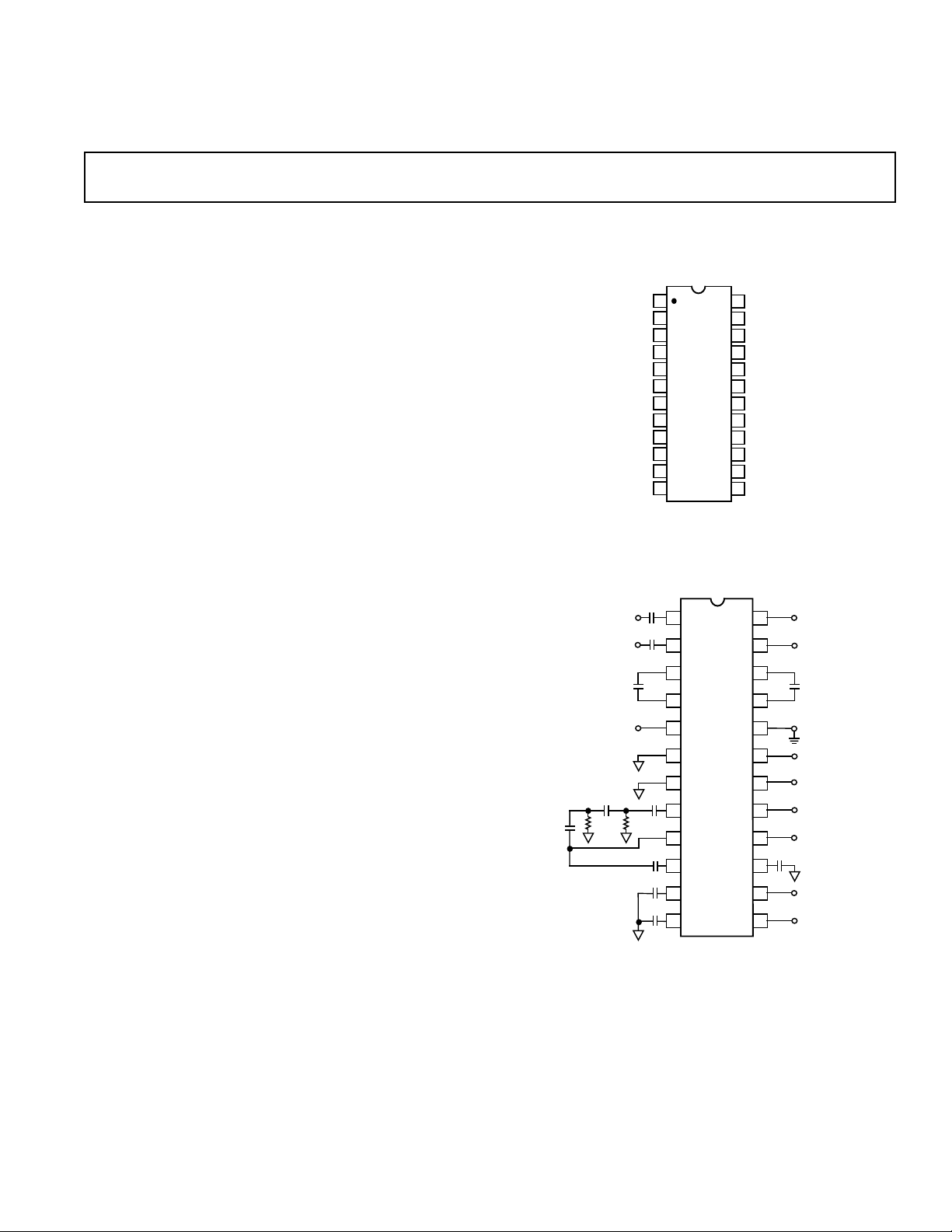
PIN CONFIGURATION
24-Lead Plastic DIP
24-Lead SOIC
1
L IN
R IN
L VCF C1
L VCF C2
V+
ACOM
VCA PORT
VCF DET IN
SUM OUT
VCA DET IN
VCF DET CAP
VCA DET CAP
2
3
4
5
SSM2000
6
TOP VIEW
(Not to Scale)
7
8
9
10
11
12
NC = NO CONNECT
24
L OUT
23
R OUT
22
R VCF C1
R VCF C2
21
20
V–
19
DIGITAL GND
NC
18
17
MUTE
DEFEAT
16
AUTO THRESHOLD CAP
15
DEFAULT THRESHOLD
14
13
NC
GENERAL DESCRIPTION
The SSM2000 is an advanced audio noise reduction system
based on proprietary HUSH
®
circuitry. HUSH combines a dynamic filter and downward expander to provide a high level of
effectiveness without the sonic artifacts normally associated with
noise reduction systems. In addition, an Adaptive Threshold
circuit detects nominal signal levels and dynamically adjusts
both thresholds, thereby providing optimal results regardless of
program source. Since it is a single-ended system, HUSH can
be used on virtually any audio source, including audio and
video tapes, radio and television broadcasts, or any other source
with objectionable noise. The SSM2000 can be used with
Dolby B
direct access to the Voltage Controlled Amplifier port enabling
additional functions such as dc volume control, automatic leveling, compression, etc. with minimal external circuitry.
Dolby B is a registered trademark of Dolby Laboratories, Inc.
HUSH is a registered trademark of Rocktron Corporation.
REV. 0
Information furnished by Analog Devices is believed to be accurate and
reliable. However, no responsibility is assumed by Analog Devices for its
use, nor for any infringements of patents or other rights of third parties
which may result from its use. No license is granted by implication or
otherwise under any patent or patent rights of Analog Devices. (See page 16.)
encoded sources with excellent results. A key feature is
Figure 1. Typical Basic Application
© Analog Devices, Inc., 1996
One Technology Way, P.O. Box 9106, Norwood, MA 02062-9106, U.S.A.
Tel: 617/329-4700 Fax: 617/326-8703
SSM2000–SPECIFICATIONS
MASKED NOISE FILTERED NOISE
AUDIO
SIGNAL
6 dB/OCTAVE SLOPE
f
C
= 3 kHz TO 37 kHz
PASSBAND FREQUENCY
RESPONSE ±0.5 dB
(VS = +8.5 V, ACOM = VS/2, f = 1 kHz, RL = 100 kV, 0 dBu = 0.775 V rms.
TA = +258C, Noise Reduction and Adaptive Threshold enabled (Pin 14 at VS/2), unless otherwise noted.)
SSM2000
Parameter Symbol Conditions Min Typ Max Units
AUDIO SIGNAL PATH
Signal-to-Noise Ratio SNR V
= 0 V, 20 Hz to 20 kHz (Flat) 80 86 dB
IN
Headroom HR Clip Point, THD = 1% 4.5 dBu
Dynamic Range Clipping to Noise Floor 91 dB
Total Harmonic Distortion THD+N V
= 300 mV rms, 2nd & 3rd Harmonics
IN
1
0.02 0.04 %
Effective Noise Reduction 20 kHz Bandwidth (Flat)
Downward Expander Section 15 dB
Dynamic Filter Section 10 dB
Input Impedance Z
Output Impedance, Dynamic Z
IN
OUT
Pins 1 and 2 6 8 kΩ
Pins 23 and 24 7 Ω
Capacitive Load No Oscillation 300 pF
Channel Separation f = 1 kHz, V
Mute Output V
= 300 mV rms –85 dB
IN
Gain Matching, L & R Channels VCA at A
= 300 mV rms 60 dB
IN
= 0 dB ±1dB
V
Gain Bandwidth GBW NR Disabled 37 kHz
DYNAMIC FILTER
Minimum Bandwidth BW
Maximum Bandwidth BW
MIN
MAX
VCF C = 0.001 µF 3 kHz
37 kHz
VCA CONTROL PORT
Input Impedance Pin 7 3.8 kΩ
VCA Voltage Gain Range A
V
VIN = 300 mV rms (Pin 7 = 2.0 V & 0 V) –70 +1 dB
Gain Constant 20 22 26 mV/dB
Control Feedthrough Pin 7 1 10 mV
POWER SUPPLY
Voltage Range V
Supply Current I
S
SY
+7.0 18 V
7.5 11 mA
Power Supply Rejection PSRR+ 70 dB
VCA, VCF DETECTOR
Input Impedance R
NOTES
1
NR in defeat mode.
Specifications subject to change without notice.
0
–10
–20
–30
–40
INPUT
–50
LEVEL
–60
–70
–80
–90
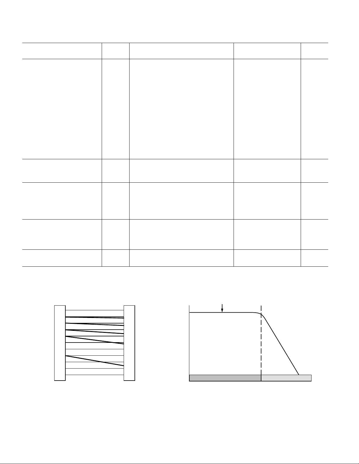
Figure 2. Downward Expander Attenuation Characteristic
–100
IN
(In dBt; 0 dBt = Threshold)
Pins 8 and 10 4.0 5.4 7.0 kΩ
0
–10
–20
–30
–40
OUTPUT
–50
LEVEL
–60
–70
–80
–90
–100
Figure 3. Dynamic Filter Characteristic (For CF = 0.001 µF
Defeat Mode)
–2–
REV. 0
PIN DESCRIPTION
WARNING!
ESD SENSITIVE DEVICE
SSM2000
Pin # Name Function and Explanation
1 L IN Left Audio Input.
2 R IN Right Audio Input.
3 L VCF C1 Left VCF Filter Cap Port.
4 L VCF C2 Left VCF Filter Cap Port.
5 V+ Positive Supply.
6 ACOM Analog Common Voltage. In-
ternal Circuit Ground Point.
Must be held to a voltage approximately halfway between
V+ and V–. Should be a clean
low impedance voltage source
capable of at least 4 mA, such
as from a buffer driven off a
supply-splitting voltage divider.
7 VCA PORT Input to VCA Control Port.
Allows external adjustment of
attenuation with a +22 mV/dB
slope. Zero volts relative to
ACOM gives zero additional
attenuation. Should be connected to ACOM if function
not required.
8 VCF DET IN Input to VCF Detector.
9 SUM OUT Combined Left Plus Right
Output.
10 VCA DET IN Input to VCA Detector.
11 VCF DET CAP Voltage Controlled Filter.
Time Constant Capacitor Port.
12 VCA DET CAP Voltage Controlled Amplifier.
Time Constant Capacitor Port.
Pin # Name Function and Explanation
13 NC Make No Connection to this
Pin.
14 DEFAULT Default Threshold Adjust-
THRESHOLD ment Port. Allows reduction
of noise reduction action if
signal source is relatively
clean such as CD sources.
Normally connected to Analog
Common. –1.2 V is recommended for CDs; –2 V completely defeats noise reduction.
15 AUTO THRESHOLD
CAP Automatic Threshold Detec-
tor Capacitor Port.
16 DEFEAT Logic High: Defeats Noise
Reduction.
Logic Low: Normal Action.
Connect to Ground if not used.
17 MUTE Logic High: Mute.
Logic Low: Normal Action.
Connect to Ground if not used.
18 NC Make no connection to this
pin.
19 DIGITAL GND Digital Logic Reference
(Logic Zero).
20 V– Negative Supply.
21 R VCF C2 Right VCF Capacitor Port.
22 R VCF C1 Right VCF Capacitor Port.
23 R OUT Right Audio Output.
24 L OUT Left Audio Output.
ABSOLUTE MAXIMUM RATINGS
Supply Voltage . . . . . . . . . . . . . . . . . . . . . . . . . . . . . . . . +18 V
Audio Input Voltage . . . . . . . . . . . . . . . . . . Supply Voltage(s)
Control Port Voltage (Pin 7) . . . . . . . . . . . . . . Positive Supply
Default Override (Pin 14) . . . . . . . . . . . . . . . . . . . . . . . . . V+
Defeat (Pin 16) . . . . . . . . . . . . . . . . . . . . . . . . . . . . . . . . . V+
Mute Override (Pin 17) . . . . . . . . . . . . . . . . . . . . . . . . . . . V+
Operating Temperature Range . . . . . . . . . . . . –40°C to +85°C
Storage Temperature Range . . . . . . . . . . . . –65°C to +150°C
Junction Temperature (T
Lead Temperature (Soldering, 60 sec) . . . . . . . . . . . . . +300°C
ESD RATINGS
883 (Human Body) Model . . . . . . . . . . . . . . . . . . . . . . 2.5 kV
EIAJ Model . . . . . . . . . . . . . . . . . . . . . . . . . . . . . . . . . . 300 V
CAUTION
ESD (electrostatic discharge) sensitive device. Electrostatic charges as high as 4000 V readily
accumulate on the human body and test equipment and can discharge without detection.
Although the SSM2000 features proprietary ESD protection circuitry, permanent damage may
occur on devices subjected to high energy electrostatic discharges. Therefore, proper ESD
precautions are recommended to avoid performance degradation or loss of functionality.
REV. 0
) . . . . . . . . . . . . . . . . . . . . . +150°C
J
ORDERING GUIDE
Temperature Package Package
Model Range Description Option
SSM2000P –40°C to +85°C 24-Pin Plastic DIP N-24
SSM2000S –40°C to +85°C 24-Pin SOIC SOL-24
PACKAGE INFORMATION
Package Type u
1
JA
u
JC
24-Pin Plastic DIP (P) 54 27 °C/W
24-Pin SOIC (S) 72 24 °C/W
NOTE
1
θJA is specified for the worst case conditions, i.e., θJA is specified for device in socket
for P-DIP packages; θJA is specified for device soldered onto a circuit board for
surface mount packages..
–3–
Units
SSM2000
DEFEAT
EXTERNAL VCA
CONTROL PORT
R
OUT
L
OUT
R
IN
L
IN
DEFAULT
THRESHOLD
VOLTAGE
CONTROLLED
FILTER
VOLTAGE
CONTROLLED
AMPLIFIER
LOGIC
INTERFACE
VOLTAGE
CONTROLLED
FILTER
VOLTAGE
CONTROLLED
AMPLIFIER
MUTE
LOGIC
INTERFACE
DIFFERENCE
AMPLIFIER
AUTO THRESHOLD
NEGATIVE PEAK
DETECTOR
HIGH-PASS
FILTER
PEAK
DETECTOR
PEAK
DETECTOR
DIFFERENCE
AMPLIFIER
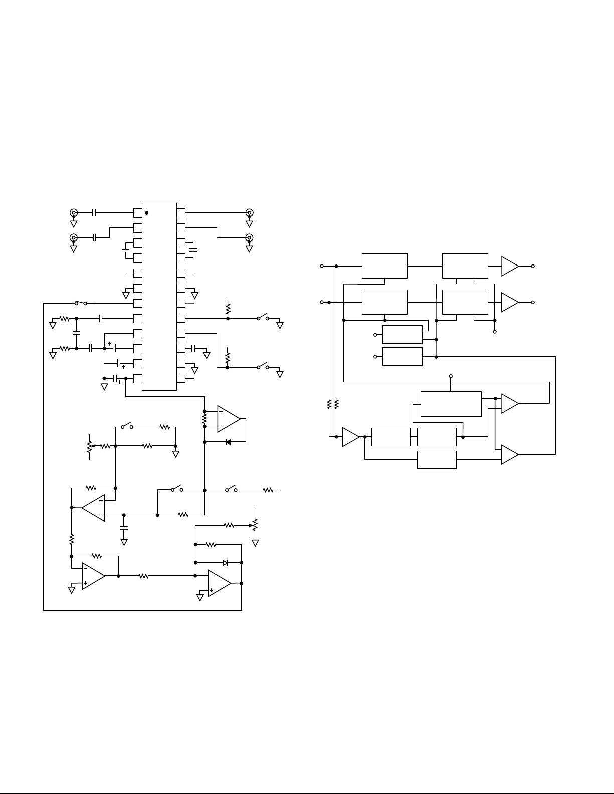
APPLICATIONS
This applications example (Figure 4) demonstrates some of the
additional functions that can be easily implemented through use
of the VCA Control Port (Pin 7). These functions can be selected
to operate simultaneously with the basic HUSH noise reduction
function. The VCA detector output provides a signal which can
be further processed using one quad op amp (OP482) to provide
these various additional useful functions.
The circuit shown in the figure below achieves: (1) Compression, (2) Volume Leveling, (3) DC Volume Adjustment.
C1
JA1
RCA
LEFT IN
JA2
RCA
RIGHT IN
THRESHOLD
20kΩ
Figure 4. Typical Dual Supply Application and Test Circuit
6.8µF
6.8µF
SW1-F
SIDE CHAIN
OPEN = OUT
CLOSED = IN
R1
C5
1kΩ
0.022µF
R2
C6
510Ω
0.022µF
10%
+5V
LEVEL
R7, 10kΩ
PT10V
–5V
R11
12kΩ
14
U1-D
OP482
R12
9
10
C2
0.001µF
C4
0.0022µF
3.3µF
SW1-A
OPEN = COMP
CLOSED = LEVEL
R8
20kΩ
13
12
R13
20kΩ
8
U1-C
OP482
1
2
3
C3
4
5
+5V
6
7
8
9
C7
2.2µF
10
C8
1µF
11
12
C9
R10
5.1kΩ
C12
1µF NON-POLARIZED
10% POLY, 63V
R17
20kΩ
SSM2000
R9
7.5kΩ
SW1-D
OPEN = LEVEL
CLOSED = COMP
24
23
22
21
20
19
18
17
16
15
14
13
R14
100kΩ
R16
1.5MΩ
–5V
NC
C11
0.22µF
NC
C10
0.001µF
+5V
+5V
3
2
1N4148
SW1-E
OPEN = LEVEL
CLOSED = COMP
R18
30kΩ
R19
20kΩ
D2
1N4148
6
5
U1-B
OP482
R3
3kΩ
R4
3kΩ
U1-A
OP482
7
1
JA3
RCA
LEFT OUT
JA4
RCA
RIGHT OUT
SW1-C
MUTE
OPEN = MUTE
CLOSED = OFF
SW1-B
BYPASS
OPEN = BYPASS
CLOSED = HUSH
R15
10MΩ
–5V
VOLUME
CONTROL
VR1, 10kΩ
LINEAR
SIMPLIFIED THEORY OF OPERATION
The input audio signals are processed to extract information
concerning the frequency distribution and amplitude of both
the desired signals and the undesired noise. Left and right audio signals are passed through voltage controlled (low-pass) filter, and then through a voltage controlled amplifiers. Both the
filters and amplifiers are low distortion, and add negligible noise
of their own. The VCF has a user-definable cutoff range that is
usually set from 1 kHz to 35 kHz. It can be set to cover other
ranges as required by the application. The VCA can be adjusted
from a loss to a gain, adding to the SSM2000’s versatility. In
accordance with proprietary patented algorithms, control signals are derived and applied to both the VCF and VCA, resulting in up to 25 dB noise suppression with the minimum loss of
desired signals.
–5V
Figure 5. SSM2000 System Block Diagram
–4–
REV. 0
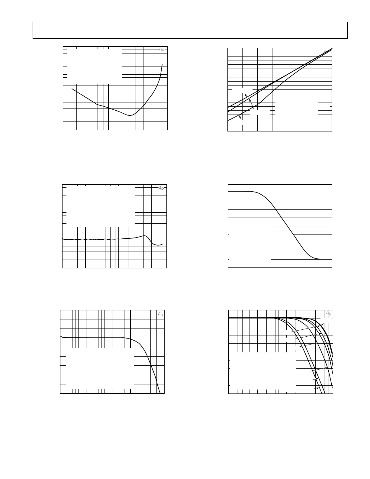
T ypical Performance Characteristics–SSM2000
10
TA = +25°C
VS = ± 4.25V (Pin 5, 20)
DEF THRESHOLD = 0V (Pin 14)
DEFEAT = ON (Pin 16)
MUTE = OFF (Pin 17)
1
= 100kΩ
R
L
BOTH CHANNELS
THD + N – %
0.1
0.01
0.01 20.1
INPUT SIGNAL – V
rms
Figure 6. THD+N (%) vs. Input Signal
1
TA = +25°C
V
= ± 4.25V (Pin 5, 20)
S
= 300mV
rms
V
IN
DEF THRESHOLD = 0V (Pin 14)
DEFEAT = ON (Pin 16)
0.1
MUTE = OFF (Pin 17)
= 100kΩ
R
L
BOTH CHANNELS
THD + N – %
0.01
0.001
20 30k100
SINE WAVE (Pin 1, 2)
1k 10k
FREQUENCY – Hz
0
–10
–20
–30
–40
V
TH
V
–70 0–60
= –2.0V
V
TH
= 0V
TH
–50 –40 –30 –20 –10
TA = +25°C
VS = ± 4.25V (Pin 5, 20)
DEF THRESHOLD = 0V (Pin 14)
DEFEAT = OFF (Pin 16)
= –1.2V
MUTE = OFF (Pin 17)
= 100kΩ
R
L
0dBu = 0.775mV
INPUT SIGNAL – dBu
@ 1kHz
rms
–50
–60
–70
OUTPUT SIGNAL – dBu
–80
–90
1
–100
Figure 9. Output vs. Input Characteristics (With Different
Adaptive Threshold Voltage, Pin 17)
10
0
–10
–20
–30
–40
TA = +25°C
V
= ± 4.25V (Pin 5, 20)
S
–50
= 300mV
rms
V
IN
–60
DEF THRESHOLD = 0V (Pin 14)
DEFEAT = OFF (Pin 16)
L, R CHANNEL OUTPUT – dB
–70
MUTE = OFF (Pin 17)
= 100kΩ
R
L
–80
BOTH CHANNELS
–90
–1 3–0.5
SINE WAVE (Pin 1, 2)
0 0.5 1 1.5 2 2.5
VCA CONTROL VOLTAGE (Pin 7) – V
REV. 0
Figure 7. THD+N (%) vs. Frequency
6
4
2
0
–2
TA = +25°C
VS = ± 4.25V (Pin 5, 20)
–4
GAIN – dB
–6
–8
–10
–12
= 300mV
rms
V
IN
DEF THRESHOLD = 0V (Pin 14)
DEFEAT = ON (Pin 16)
MUTE = OFF (Pin 17)
= 100kΩ
R
L
BOTH CHANNELS
20 200k100
SINE WAVE (Pin 1, 2)
1k 10k 100k
FREQUENCY – Hz
Figure 8. –3 dB Bandwidth
Figure 10a. Channel Output vs. VCA Control Voltage (Pin 7)
3.00
0.7
–1.6
–3.9
–6.2
–8.5
TA = +25°C
–10.8
V
GAIN – dB
–13.1
–15.4
–17.7
–20.0
= ± 4.25V (Pin 5, 20)
S
= 300mVrms SINE WAVE (Pin 1, 2)
V
IN
DEF THRESHOLD = 0V (Pin 14)
DEFEAT = OFF (Pin 16)
MUTE = OFF (Pin 17)
R
= 100kΩ
L
20 80k100
40kHz
20kHz
8kHz
6kHz
4kHz
100 – 2kHz MIN BW
1k 10k
FREQUENCY – Hz
50kHz
Figure 10b. VFC Characteristics (Simulated Noise Level
90 mV rms with Different Frequency) Applied through a
3-Pole HP filter
–5–
 Loading...