Low-Power, High-Precision
a
FEATURES
Low Supply Current: 600 A Max
OP07 Type Performance
Offset Voltage: 20 V Max
Offset Voltage Drift: 0.6 V/ⴗ C Max
Very Low Bias Current
25ⴗC: 100 pA Max
–55ⴗC to +125ⴗC: 250 pA Max
High Common-Mode Rejection: 114 dB Min
Extended Industrial Temperature Range: –40ⴗC to +85ⴗC
Available In Die Form
GENERAL DESCRIPTION
The OP97 is a low power alternative to the industry-standard
OP07 precision amplifier. The OP97 maintains the standards of
performance set by the OP07 while utilizing only 600 µA supply
current, less than 1/6 that of an OP07. Offset voltage is an
ultralow 25 µV, and drift over temperature is below 0.6 µV/°C.
External offset trimming is not required in the majority of circuits.
Improvements have been made over OP07 specifications in
several areas. Notable is bias current, which remains below
250 pA over the full military temperature range. The OP97 is
ideal for use in precision long-term integrators or sample-andhold circuits that must operate at elevated temperatures.
Common-mode rejection and power supply rejection are also
improved with the OP97, at 114 dB minimum over wider
ranges of common-mode or supply voltage. Outstanding
PSR, a supply range specified from ±2.25 V to ±20 V and the
OP97’s minimal power requirements combine to make the
OP97 a preferred device for portable and battery-powered
instruments.
The OP97 conforms to the OP07 pinout, with the null potentiometer connected between Pins 1 and 8 with the wiper to V+.
The OP97 will upgrade circuit designs using 725, OP05, OP07,
OP12, and 1012 type amplifiers. It may replace 741-type amplifiers in circuits without nulling or where the nulling circuitry has
been removed.
Operational Amplifier
OP97
PIN CONNECTIONS
Epoxy Mini-DIP (P Suffix)
8-Pin Cerdip
(Z Suffix)
8-Pin SO (S Suffix)
NULL
–IN
+IN
1
OP97
2
3
V–
4
8
7
6
5
NULL
V+
OUT
OVER
COMP
REV. D
Information furnished by Analog Devices is believed to be accurate and
reliable. However, no responsibility is assumed by Analog Devices for its
use, nor for any infringements of patents or other rights of third parties that
may result from its use. No license is granted by implication or otherwise
under any patent or patent rights of Analog Devices.
One Technology Way, P.O. Box 9106, Norwood, MA 02062-9106, U.S.A.
Tel: 781/329-4700 www.analog.com
Fax: 781/326-8703 © Analog Devices, Inc., 2002

OP97–SPECIFICATIONS
ELECTRICAL CHARACTERISTICS
Parameter Symbol Conditions Min Typ Max Min Typ Max Unit
Input Offset Voltage V
OS
(@ VS = ⴞ15 V, V
= 0 V, TA = 25ⴗC, unless otherwise noted.)
CM
OP97A/E OP97F
10 25 30 75 µV
Long-Term Offset
Voltage Stability ∆V
Input Offset Current I
Input Bias Current I
Input Noise Voltage e
Input Noise Voltage Density e
Input Noise Current Density i
Large-Signal Voltage Gain A
Common-Mode Rejection CMR V
Power-Supply Rejection PSR V
/Time 0.3 0.3 µV/Month
OS
OS
B
p-p 0.1 Hz to 10 Hz 0.5 0.5 µV p-p
n
n
n
VO
fO = 10 Hz
= 1000 Hz
f
O
fO = 10 Hz 20 20 fA/√Hz
VO = ±10 V; RL = 2 kΩ 300 2000 200 2000 V/mV
CM
= ±2 V to ±20 V 114 132 110 132 dB
S
2
3
= ±13.5 V 114 132 110 132 dB
30 100 30 150 pA
±30 ± 100 ±30 ± 150 pA
17 30 17 30 nV/√Hz
14 22 14 22 nV/√Hz
Input Voltage Range IVR (Note 1) ±13.5 ±14.0 ±13.5 ±14.0 V
Output Voltage Swing V
O
RL = 10 kΩ±13 ± 14 ± 13 ±14 V
Slew Rate SR 0.1 0.2 0.1 0.2 V/µs
Differential Input Resistance R
IN
Closed-Loop Bandwidth BW A
Supply Current I
Supply Voltage V
NOTES
1
Guaranteed by CMR test.
2
10 Hz noise voltage density is sample tested. Devices 100% tested for noise are available on request.
3
Sample tested.
4
Guaranteed by design.
Specifications subject to change without notice.
SY
S
(Note 4) 30 30 MΩ
= 1 0.4 0.9 0.4 0.9 MHz
VCL
380 600 380 600 µA
Operating Range ±2 ±15 ± 20 ±2 ± 15 ± 20 V
(@ VS = ⴞ15 V, VCM = 0 V, –40ⴗC ≤ TA ≤ +85ⴗC for the OP97E/F and –55ⴗC ≤ TA ≤ +125ⴗC
ELECTRICAL CHARACTERISTICS
for the OP97A, unless otherwise noted.)
OP97A/E OP97F
Parameter Symbol Conditions Min Typ Max Min Typ Max Unit
Input Offset Voltage VOS 25 60 60 200 µV
Average Temperature TCV
Coefficient of V
Input Offset Current I
OS
OS
Average Temperature TCI
Coefficient of I
Input Bias Current I
OS
B
OS
OS
S-Package 0.2 0.6 0.3 2.0 µV/°C
0.3
60 250 80 750 pA
0.4 2.5 0.6 7.5 pA/°C
±60 ± 250 ± 80 ± 750 pA
Average Temperature
Coefficient of I
B
Large Signal Voltage Gain A
TCI
VO
B
Common-Mode Rejection CMR V
Power Supply Rejection PSR V
VO = 10 V; RL = 2 kΩ 200 1000 150 1000 V/mV
= ±13.5 V 108 128 108 128 dB
CM
= ±2.5 V to ±20 V 108 126 108 128 dB
S
0.4 2.5 0.6 7.5 pA/°C
Input Voltage Range IVR (Note 1) ±13.5 ±14.0 ±13.5 ± 14.0 V
Output Voltage Swing V
O
RL = 10 kΩ±13 ± 14 ±13 ± 14 V
Slew Rate SR 0.05 0.15 0.05 0.15 V/µs
Supply Current I
Supply Voltage V
NOTES
1
Guaranteed by CMR test.
Specifications subject to change without notice.
SY
S
Operating Range ±2.5 ±15 ± 20 ± 2.5 ±15 ± 20 V
400 800 400 800 µA
–2–
REV. D

OP97
WARNING!
ESD SENSITIVE DEVICE
ABSOLUTE MAXIMUM RATINGS
Supply Voltage . . . . . . . . . . . . . . . . . . . . . . . . . . . . . . . ±20 V
Input Voltage
Differential Input Voltage
Differential Input Current
2
. . . . . . . . . . . . . . . . . . . . . . . . . . . . . . . ±20 V
3
. . . . . . . . . . . . . . . . . . . . . . ±1 V
3
. . . . . . . . . . . . . . . . . . . . ±10 mA
1
Output Short-Circuit Duration . . . . . . . . . . . . . . . . Indefinite
Operating Temperature Range
OP97A (Z) . . . . . . . . . . . . . . . . . . . . . . . . –55°C to +125°C
OP97E, F (P, Z, S) . . . . . . . . . . . . . . . . . . –40°C to +85°C
Storage Temperature Range . . . . . . . . . . . . –65°C to +150°C
Junction Temperature Range . . . . . . . . . . . . –65°C to +150°C
Lead Temperature (Soldering, 60 sec) . . . . . . . . . . . . 300°C
Package Type
4
JA
JC
Unit
8-Lead Hermetic DIP (Z) 148 16 °C/W
8-Lead Plastic DIP (P) 103 43 °C/W
8-Lead SO (S) 158 43 °C/W
NOTES
1
Absolute maximum ratings apply to both DICE and packaged parts, unless
otherwise noted.
2
For supply voltages less than ± 20 V, the absolute maximum input voltage is equal
to the supply voltage.
3
The OP97’s inputs are protected by back-to-back diodes. Current-limiting resis-
tors are not used in order to achieve low noise. Differential input voltages greater
than 1 V will cause excessive current to flow through the input protection diodes
unless limiting resistance is used.
4
θJA is specified for worst case mounting conditions, i.e., θJA is specified for device
in socket for TO, cerdip, and P-DIP packages; θJA is specified for device soldered
to printed circuit board for SO package.
ORDERING GUIDE
Temperature Package
Model Range Option
OP97AZ
OP97ARC/883
OP97EJ
OP97EZ
OP97EP –40°C to +85°C 8-Lead Plastic DIP
OP97FZ
3
3
3
3
–55°C to +125°C 8-Lead Cerdip
2, 3
–55°C to +125°C 20-Contact LCC
–40°C to +85°C TO-99
–40°C to +85°C 8-Lead Cerdip
–40°C to +85°C 8-Lead Cerdip
1
OP97FP –40°C to +85°C 8-Lead Plastic DIP
OP97FS –40°C to +85°C 8-Lead SOIC
OP97FS-REEL –40°C to +85°C 8-Lead SOIC
OP97FS-REEL7 –40°C to +85°C 8-Lead SOIC
NOTES
1
For outline information see Package Information section.
2
For devices processed in total compliance to MIL-STD-883, add /883 after
part number. Consult factory for /883 data sheet.
3
Not for new designs; obsolete April 2002.
For Military processed devices, please refer to the Standard
Microcircuit Drawing (SMD) available at
www.dscc.dla.mil/programs/milspec/default.asp
SMD Part Number ADI Equivalent
59628954401PA OP97AZMDA
59628954401GA
*
Not for new designs; obsolete April 2002.
*
OP97AJMDA
CAUTION
ESD (electrostatic discharge) sensitive device. Electrostatic charges as high as 4000 V readily
accumulate on the human body and test equipment and can discharge without detection. Although
the OP97 features proprietary ESD protection circuitry, permanent damage may occur on devices
subjected to high-energy electrostatic discharges. Therefore, proper ESD precautions are
recommended to avoid performance degradation or loss of functionality.
REV. D
–3–

OP97
–Typical Performance Characteristics
400
1894 UNITS
300
200
NUMBER OF UNITS
100
0
–40
–20 0 20 40
INPUT OFFSET VOLTAGE – V
VS = 15V
T
= 25 C
A
V
= 0V
CM
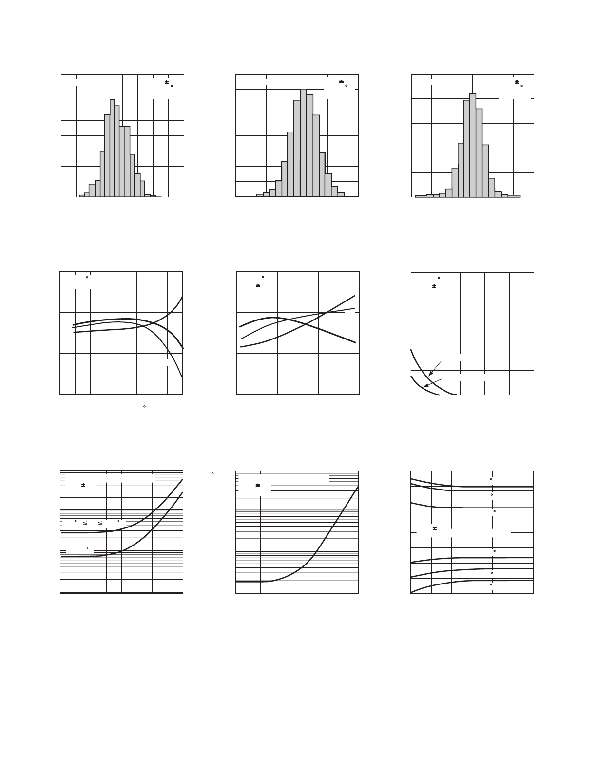
TPC 1. Typical Distribution of Input
Offset Voltage
60
TA = 25 C
V
= 0V
CM
40
20
0
–20
INPUT CURRENT - pA
–40
–60
–75
–25 0 25 50–50 75
TEMPERATURE –
C
IB–
IB+
I
OS
100 125
400
1920 UNITS
300
200
NUMBER OF UNITS
100
0
–100
–50 0 50 100
INPUT BIAS CURRENT – pA
VS = 15V
T
= 25 C
A
V
= 0V
CM
TPC 2. Typical Distribution of Input
Bias Current
60
TA = 25 C
V
= 15V
S
40
20
0
–20
INPUT CURRENT - pA
–40
–60
–15
COMMON-MODE VOLTAGE – Volts
–50 510–10 15
IB–
IB+
I
OS
500
1894 UNITS
400
300
200
NUMBER OF UNITS
100
0
–60
–40 60
INPUT OFFSET CURRENT – pA
–20 0 20 40
VS = 15V
T
= 25 C
A
V
= 0V
CM
TPC 3. Typical Distribution of Input
Offset Current
ⴞ5
TA = 25 C
V
= 15V
S
V
= 0V
CM
ⴞ4
ⴞ3
ⴞ2
J PACKAGES
ⴞ1
DEVIATION FROM FINAL VALUE – V
0
0
Z, P PACKAGES
234 5
1
TIME AFTER POWER APPLIED – Minutes
TPC 4. Input Bias, Offset Current
vs. Temperature
1000
BALANCED OR UNBALANCED
V
= 15V
S
V
= 0V
CM
100
–55 C TA +125 C
10
TA = 25 C
EFFECTIVE OFFSET VOLTAGE – V
1
3k 10k 30k 100k 1M300k 3M 10M
1k
SOURCE RESISTANCE – ⍀
TPC 7. Effective Offset Voltage vs.
Source Resistance
TPC 5. Input Bias, Offset Current
vs. Common-Mode Voltage
100
BALANCED OR UNBALANCED
V
= 15V
S
V
= 0V
CM
10
1
0.1
EFFECTIVE OFFSET VOLTAGE DRIFT – V/ C
10k 100k 1M 10M
1k
SOURCE RESISTANCE – ⍀
TPC 8. Effective TCVOS vs. Source
Resistance
100M
TPC 6. Input Offset Voltage
Warm-Up Drift
20
15
10
5
VS = 15V
0
OUTPUT SHORTED TO GROUND
–5
–10
SHORT CIRCUIT CURRENT - mA
–15
–20
0
TIME FROM OUTPUT SHORT – Minutes
TA = –55 C
TA = +25 C
TA = +125 C
TA = +125 C
TA = +25 C
TA = –55 C
123
TPC 9. Short Circuit Current vs.
Time, Temperature
–4–
REV. D
 Loading...