Low Noise, Precision, High Speed
8
7
6
5
1
2
3
4
NC = NO CONNECT
V
OS
TRIM
–IN
+IN
V
OS
TRIM
V+
OUT
NCV–
OP37
a
FEATURES
Low Noise, 80 nV p-p (0.1 Hz to 10 Hz)
3 nV/÷Hz @ 1 kHz
Low Drift, 0.2 V/C
High Speed, 17 V/s Slew Rate
63 MHz Gain Bandwidth
Low Input Offset Voltage, 10 V
Excellent CMRR, 126 dB (Common-Voltage @ 11 V)
High Open-Loop Gain, 1.8 Million
Replaces 725, OP-07, SE5534 In Gains > 5
Available in Die Form
GENERAL DESCRIPTION
The OP37 provides the same high performance as the OP27,
but the design is optimized for circuits with gains greater than
five. This design change increases slew rate to 17 V/ms and
gain-bandwidth product to 63 MHz.
The OP37 provides the low offset and drift of the OP07
plus higher speed and lower noise. Offsets down to 25 mV and
a
maximum drift
sion
instrumentation applications. Exceptionally low noise
=
3.5 nV/ @ 10 Hz), a low 1/f noise corner frequency of
(e
n
2.7 Hz,
and the high gain of 1.8 million, allow accurate
high-gain amplification of low-level signals.
The low input bias current of 10 nA and offset current of 7 nA
are achieved by using a bias-current cancellation circuit.
the military temperature range this typically holds I
to 20 nA and 15 nA respectively.
of 0.6 mV/∞C make the OP37 ideal for preci-
Over
and I
B
OS
Operational Amplifier (A
VCL
> 5)
OP37
The output stage has good load driving capability. A guaranteed
swing of 10 V into 600 W and low output distortion make the
OP37 an excellent choice for professional audio applications.
PSRR and CMRR exceed 120 dB. These characteristics, coupled
with long-term drift of 0.2 mV/month, allow the circuit
to achieve performance levels previously attained only by
discrete designs.
Low-cost, high-volume production of the OP37 is achieved
using on-chip zener-zap trimming. This reliable and stable
trimming scheme has proved its effectiveness over many
production history.
The OP37 brings low-noise instrumentation-type performance
such diverse applications as microphone, tapehead, and RIAA
phono preamplifiers, high-speed signal conditioning for data
acquisition systems, and wide-bandwidth instrumentation.
PIN CONNECTIONS
8-Lead Hermetic DIP
(Z Suffix)
Epoxy Mini-DIP
(P Suffix)
8-Lead SO
(S Suffix)
designer
by
offset
years of
to
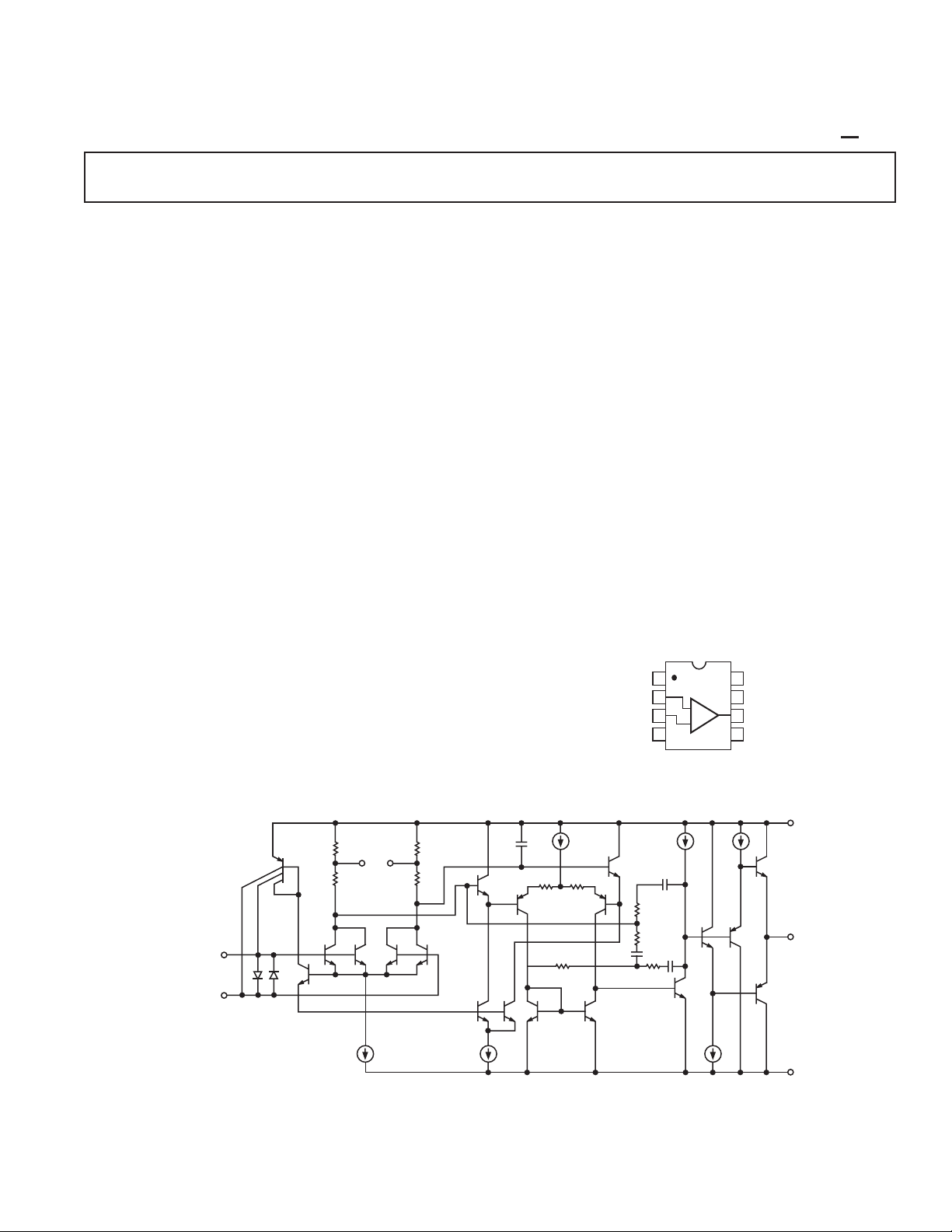
SIMPLIFIED SCHEMATIC
V+
C2
Q21
Q23
Q27 Q28
R23 R24
R5
Q24
Q22
C1
R9
R12
C3 C4
Q20 Q19
Q26
Q46
OUTPUT
Q45
V–
NON-INVERTING
INPUT (+)
INVERTING
INPUT (–)
R1 AND R2 ARE PERMANENTLY
*
ADJUSTED AT WAFER TEST FOR
MINIMUM OFFSET VOLTAGE.
Q6
Q3
R1*
R3
18
ADJ.
V
OS
Q2B
R4
R2*
Q2AQ1A Q1B
Q11 Q12
REV. B
Information furnished by Analog Devices is believed to be accurate and
use, nor for any infringements of patents or other rights of third parties that
may result from its use. No license is granted by implication or otherwise
under any patent or patent rights of Analog Devices.
reliable. However, no responsibility is assumed by Analog Devices for its
One Technology Way, P.O. Box 9106, Norwood, MA 02062-9106, U.S.A.
Tel: 781/329-4700 www.analog.com
Fax: 781/326-8703 © Analog Devices, Inc., 2002
OP37
WARNING!
ESD SENSITIVE DEVICE
ABSOLUTE MAXIMUM RATINGS
4
Supply Voltage . . . . . . . . . . . . . . . . . . . . . . . . . . . . . . . . . . 22 V
Internal Voltage (Note 1 ) . . . . . . . . . . . . . . . . . . . . . . . . . 22 V
Output Short-Circuit Duration . . . . . . . . . . . . . . . . . Indefinite
Differential Input Voltage (Note2) . . . . . . . . . . . . . . . . . 0.7 V
Differential Input Current (Note 2) . . . . . . . . . . . . . . . . 25 mA
Storage Temperature Range . . . . . . . . . . . . . –65∞C to +150∞C
Operating Temperature Range
OP37A . . . . . . . . . . . . . . . . . . . . . . . . . . . . –55∞C to +125∞C
OP37E (Z) . . . . . . . . . . . . . . . . . . . . . . . . . . –25∞C to +85∞C
OP37E, OP-37F (P) . . . . . . . . . . . . . . . . . . . . . 0∞C to 70∞C
OP37G (P, S, Z) . . . . . . . . . . . . . . . . . . . . . –40∞C to +85∞C
Lead Temperature Range (Soldering, 60 sec) . . . . . . . . 300∞C
Junction Temperature . . . . . . . . . . . . . . . . . . –45∞C to +150∞C
Package Type
3
JA
Unit
JC
8-Lead Hermetic DIP (Z) 148 16 ∞C/W
8-Lead Plastic DIP (P) 103 43 ∞C/W
8-Lead SO (S) 158 43 ∞C/W
NOTES
1
For supply voltages less than 22 V, the absolute maximum input voltage is equal
to the supply voltage.
2
The OP37’s inputs are protected by back-to-back diodes. Current limiting resistors
are not used in order to achieve low noise. If differential input voltage exceeds 0.7 V,
the input Current should be limited to 25 mA.
3
JA is specified for worst case mounting conditions, i.e., JA is specified for device
in socket for TO, CerDIP, P-DIP, and LCC packages; JA is specified for device
soldered to printed circuit board for SO package.
4
Absolute maximum ratings apply to both DICE and packaged parts, unless
otherwise noted.
ORDERING GUIDE
TA = 25∞COperating
MAX CerDIP Plastic Temperature
V
OS
(V) 8-Lead 8-Lead Range
25 OP37AZ* MIL
25 OP37EZ OP37EP IND/COM
60 OP37FP* IND/COM
100 OP37GP XIND
100 OP37GZ OP37GS XIND
*Not for new design, obsolete, April 2002.
CAUTION
ESD (electrostatic discharge) sensitive device. Electrostatic charges as high as 4000 V readily
accumulate on the human body and test equipment and can discharge without detection. Although
the OP37 features proprietary ESD protection circuitry, permanent damage may occur on
devices subjected to high-energy electrostatic discharges. Therefore, proper ESD precautions
are recommended to avoid performance degradation or loss of functionality.
–2–
REV. B
OP37
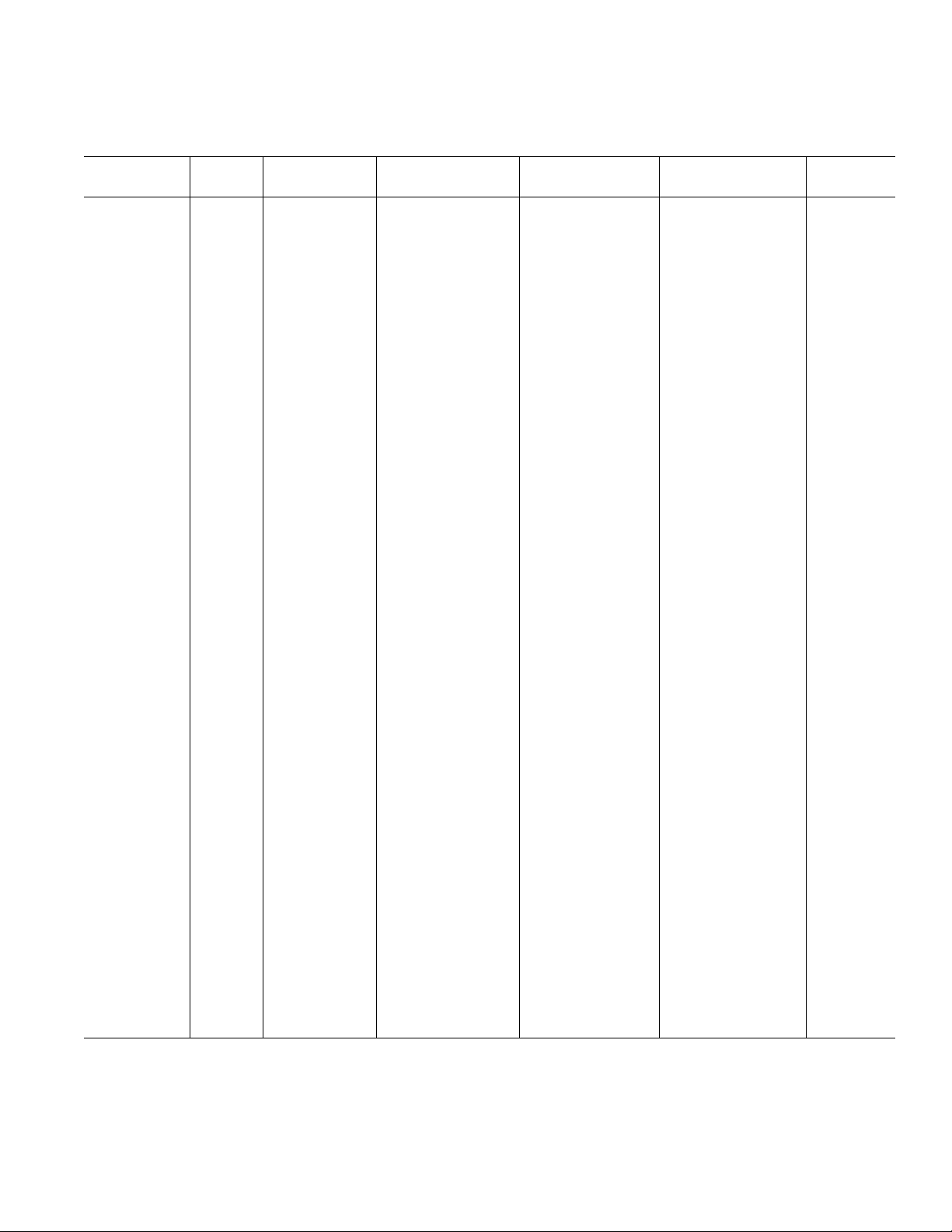
SPECIFICATIONS
( VS = 15 V, TA = 25C, unless otherwise noted.)
OP37A/E OP37F OP37G
Parameter Symbol Conditions Min Typ Max Min Typ Max Min Typ Max Unit
Input Offset
Voltage V
OS
Note 1 10 25 20 60 30 100 mV
Long-Term
Stability V
/Time Notes 2, 3 0.2 1.0 0.3 1.5 0.4 2.0 mV/Mo
OS
Input Offset
Current I
OS
735 950 12 75 nA
Input Bias
Current I
Input Noise
Voltage e
Input Noise
Voltage Density e
Input Noise
Current Density i
B
np-p
n
N
1 Hz to 10 Hz
fO = 10 Hz
= 30 Hz
f
O
= 1000 Hz
f
O
fO = 10 Hz
f
= 30 Hz
O
= 1000 Hz
f
O
3
3
3, 6
3, 6
3, 5
3
3, 6
±10 ±40 ±12 ± 55 ± 15 ± 80 nA
0.08 0.18 0.08 0.18 0.09 0.25 mV p-p
3.5 5.5 3.5 5.5 3.8 8.0
3.1 4.5 3.1 4.5 3.3 5.6 nV/÷ Hz
3.0 3.8 3.0 3.8 3.2 4.5
1.7 4.0 1.7 4.0 1.7
1.0 2.3 1.0 2.3 1.0 pA/÷ Hz
0.4 0.6 0.4 0.6 0.4 0.6
Input Resistance
Differential
Mode R
IN
Note 7 1.3 6 0.9 4 5 0.7 4 MW
Input Resistance
Common Mode
R
INCM
3 2.5 2 GW
Input Voltage
Range IVR ±11 ±12.3 ±11 ± 12.3 ±11 ±12.3 V
Common Mode
Rejection Ratio
CMRR VCM = ±11 V 114 126 106 123 100 120 dB
Power Supply
Rejection Ratio
PSSR VS = ±4 V 1 10 1 10 2 20 mV/ V
to ±18 V
Large Signal
Voltage Gain A
VO
RL ≥ 2 kW,
= ±10 V 1000 1800 1000 1800 700 1500 V/mV
V
O
R
≥ 1 kW,
L
Vo = ±10 V 800 1500 800 1500 400 1500 V/mV
R
≥ 600 W,
L
= ±1 V,
V
O
4
V
S
±4
250 700 250 700 200 500 V/mV
Output Voltage
Swing V
O
Slew Rate SR R
Gain Bandwidth
Product GBW f
RL ≥ 2 kW±12.0 ± 13.8 ± 12.0 ±13.8 ±11.5 ± 13.5 V
≥ 600 W±10 ±11.5 ±10 ± 11.5 ±10 ±11.5 V
R
L
L
= 10 kHz
O
= 1 MHz 40 40 40 MHz
f
O
≥ 2k W
4
11 17 11 17 11 17 V/ms
4
45 63 45 63 45 63 MHz
Open-Loop
Output Resistance
R
O
VO = 0, IO = 0 70 70 70 W
Power
Consumption P
d
VO = 0 90 140 90 140 100 170 mW
Offset Adjustment
Range RP = 10 kW±4 ±4 ±4mV
NOTES
1
Input offset voltage measurements are performed by automated test equipment approximately 0.5 seconds after application of power. A/E grades guaranteed fully
warmed up.
2
Long term input offset voltage stability refers to the average trend line of VOS vs. Time over extended periods after the first 30 days of operation. Excluding the initial
hour of operation, changes in VOS during the first 30 days are typically 2.5 mV—refer to typical performance curve.
3
Sample tested.
4
Guaranteed by design.
5
See test circuit and frequency response curve for 0.1 Hz to 10 Hz tester.
6
See test circuit for current noise measurement.
7
Guaranteed by input bias current.
REV. B
–3–
OP37–SPECIFICATIONS
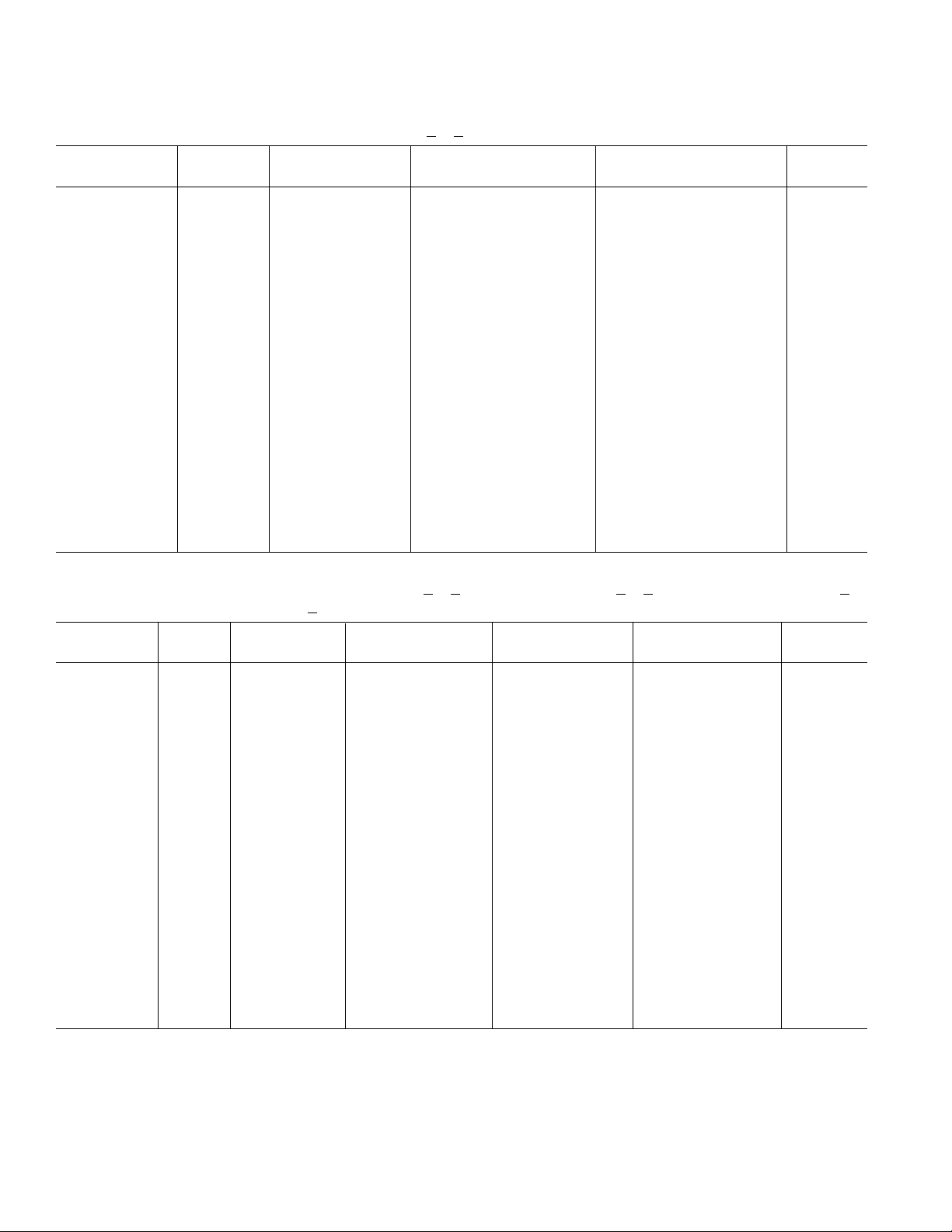
Electrical Characteristics
( VS = 15 V, –55C < TA < +125C, unless otherwise noted.)
OP37A OP37C
Parameter Symbol Conditions Min Typ Max Min Typ Max Unit
Input Offset
Voltage V
OS
Note 1 10 25 30 100 mV
Average Input
Offset Drift TCV
TCV
OS
OSN
Note 2
Note 3 0.2 0.6 0.4 1.8 mV/∞C
Input Offset
Current I
OS
15 50 30 135 nA
Input Bias
Current I
B
±20 ± 60 ±35 ±150 nA
Input Voltage
Range IVR ±10.3 ± 11.5 ±10.2 ± 11.5 V
Common Mode
Rejection Ratio CMRR V
= ±10 V 108 122 94 116 dB
CM
Power Supply
Rejection Ratio PSRR V
= ±4.5 V to
S
±18 V 2 16 4 51 mV/ V
Large-Signal
Voltage Gain A
VO
RL ≥ 2 kW,
V
= ±10 V 600 1200 300 800 V/mV
O
Output Voltage
Swing V
O
RL ≥ 2 kW±11.5 ±13.5 ± 10.5 ±13.0 V
(VS = 15 V, –25C < TA < +85C for OP37EZ/FZ, 0C < TA < 70C for OP37EP/FP, and –40C < T
Electrical Characteristics
< +85C for OP37GP/GS/GZ, unless otherwise noted.)
OP37E OP37F OP37C
Parameter Symbol Conditions Min Typ Max Min Typ Max Min Typ Max Unit
Input Offset
Voltage V
OS
20 50 40 140 55 220 mV
Average Input
Offset Drift TCV
TCV
Note 2
OS
Note 3 0.2 0.6 0.3 1.3 0.4 1.8 mV/∞C
OSN
Input Offset
Current I
OS
10 50 14 85 20 135 nA
Input Bias
Current I
B
±14 ±60 ±18 ±95 ± 25 ±150 nA
Input Voltage
Range IVR ±10.5 ± 11.8 ±10.5 ±11.8 ±10.5 ±11.8 V
Common Mode
Rejection Ratio CMRR V
= ±10 V 108 122 100 119 94 116 dB
CM
Power Supply
Rejection Ratio PSRR V
= ±4.5 V to
S
±18 V 2 15 2 16 4 32 mV/ V
Large-Signal
Voltage Gain A
VO
RL ≥ 2 kW,
= ±10 V 750 1500 700 1300 450 1000 V/mV
VO
Output Voltage
Swing V
NOTES
1
Input offset voltage measurements are performed by automated test equipment approximately 0.5 seconds after application of power. A/E grades guaranteed fully
warmed up.
2
The TC
3
Guaranteed by design.
performance is within the specifications unnulled or when nulled withRP = 8 kW to 20 kW. TC
VOS
O
RL ≥ 2 kW±11.7 ± 13.6 ±11.4 ±13.5 ±11 ±13.3 V
is 100% tested for A/E grades, sample tested for F/G grades.
VOS
A
–4–
REV. B
OP37
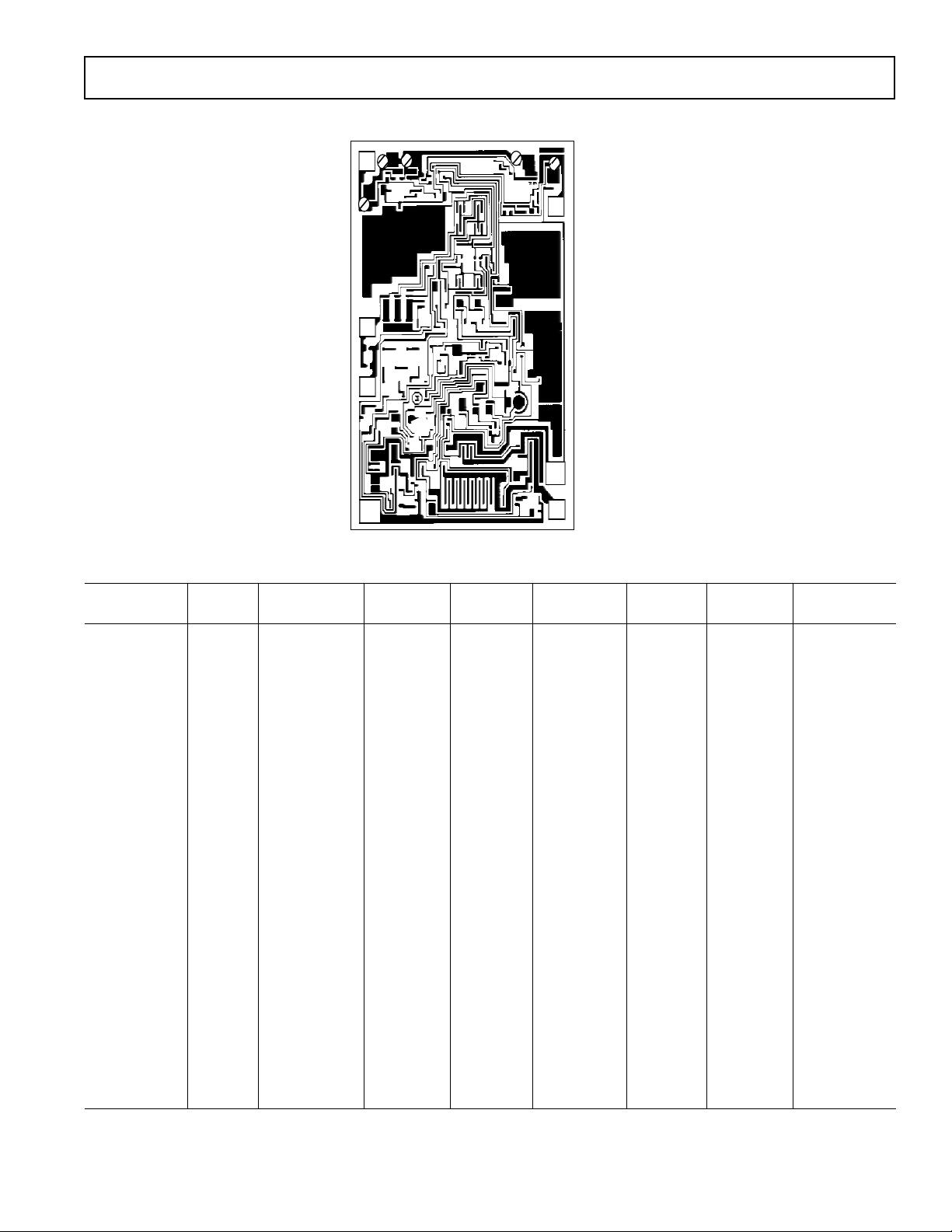
BINDING DIAGRAM
1. NULL
8
7
2. (–) INPUT
3. (+) INPUT
4. V–
6. OUTPUT
7. V+
8. NULL
1
1990
1427U
2
3
4
6
(VS = 15 V, TA = 25C for OP37N, OP37G, and OP37GR devices; TA = 125C for OP37NT and OP37GT devices,
Wafer Test Limits
unless otherwise noted.)
OP37NT OP37N OP37GT OP37G OP37GR
Parameter Symbol Conditions Limit Limit Limit Limit Limit Unit
Input Offset
Voltage V
OS
Note 1 60 35 200 60 100 mV MAX
Input Offset
Current I
OS
50 35 85 50 75 nA MAX
Input Bias
Current I
B
±60 ± 40 ± 95 ±55 ± 80 nA MAX
Input Voltage
Range IVR ±10.3 ±11 ± 10.3 ± 11 ± 11 V MIN
Common Mode
Rejection Ratio CMRR V
= ±11 V 108 114 100 106 100 dB MIN
CM
Power Supply
Rejection Ratio PSRR T
= 25∞C,
A
V
= ±4 V to
S
±18 V 10 10 101020mV/V MAX
= 125∞C,
T
A
V
= ±4.5 V to
S
±18 V 16 20 mV/V MAX
Large-Signal
Voltage Gain A
VO
RL ≥ 2 kW,
= ±10 V 600 1000 500 1000 700 V/mV MIN
V
O
R
≥ 1 kW,
L
V
= ±10 V 800 800 V/mV MIN
O
Output Voltage
Swing V
O
RL ≥ 2 kW±11.5 ±12 ± 11 ±12 ±11.5 V MIN
R
≥ 600 kW±10 ±10 ±10 V MIN
L
Power
Consumption P
NOTES
For 25∞C characterlstics of OP37NT and OP37GT devices, see OP 37N and OP37G characteristics, respectively.
Electrical tests are performed at wafer probe to the limits shown. Due to variations in assembly methods and normal yield loss, yield after packaging is not guaranteed
for standard product dice. Consult factory to negotiate specifications based on dice lot qualification through sample lot assembly and testing.
d
REV. B
VO = 0 140 140 170 mW MAX
–5–
 Loading...