

Page 1

Engineer-to-Engineer Note EE-264
a
Technical notes on using Analog Devices DSPs, processors and development tools
Contact our technical support at dsp.support@analog.com and at dsptools.support@analog.com
Or vi sit our o n-li ne r esou rces htt p:/ /www.analog.com/ee-notes and http://www.analog.com/processors
Interfacing MultiMediaCard™ with ADSP-2126x SHARC® Processors
Contributed by Aseem Vasudev Prabhugaonkar and Jagadeesh Rayala Rev 1 – March 11, 2005
Introduction
This application note describes how to
implement the interface between an ADSP2126x SHARC® processor and a
MultiMediaCard™ (MMC). The application note
also describes the MMC command format and
demonstrates with example code how an MMC
card can be interfaced seamlessly with the
SHARC processor’s SPI port. Example code
supplied with this application note implements
the most commonly used commands of
MultiMediaCard.
About MultiMediaCard
memory access voltage of 2.7 to 3.6 V, and a
capacity from 4 MB to the gigabyte range.
About the ADSP-2126x SPI Port
The ADSP-2126x processor is equipped with a
synchronous serial peripheral interface port that
is compatible with the industry-standard Serial
Peripheral Interface (SPI). The SPI port supports
communication with a variety of peripheral
devices including codecs, data converters,
sample rate converters, S/PDIF or AES/EBU
digital audio transmitters and receivers, LCDs,
shift registers, micro-controllers, and FPGA
devices with SPI emulation capabilities.
The MMC was introduced in 1998 and had an
amazing reduction in cubic capacity compared
with CompactFlash™. MMC cards are now
widely used in digital cameras, smart cell
Important features of ADSP-2126x SPI port
include:
Simple four-wire interface, consisting of two
data pins, a device select pin, and a clock pin
phones, PDAs, and portable MP3 players. Their
intended use is to store information and content.
Full duplex operation, allowing simultaneous
data transmission and reception on the same
The MMC consists of a 7-pin interface and
SPI port
supports two serial data transfer protocols viz.
the MMC (MultiMediaCard) mode and SPI
(Serial Peripheral Interface) mode. The
maximum operating clock frequency used for
serial communication in both modes can go up to
20 MHz. The data written in any of these modes
can be read by host in either mode. The
advantage of MMC supporting SPI mode is that
MMC can be interfaced seamlessly to many
controllers or DSP processors, which have onchip support for SPI. Most MMCs have a
Data formats to accommodate little and big
endian data, different word lengths, and
packing modes
Master and slave modes as well as
multimaster mode in which the ADSP-2126x
processor can be connected to up to four other
SPI devices
Open drain outputs to avoid data contention
and to support multimaster scenarios
communication voltage from 2.0 to 3.6 V, a
Copyright 2005, Analog Devices, Inc. All rights reserved. Analog Devices assumes no responsibility for customer product design or the use or application of
customers’ products or for any infringements of patents or rights of others which may result from Analog Devices assistance. All trademarks and logos are property
of their respective holders. Information furnished by Analog Devices applications and development tools engineers is believed to be accurate and reliable, however
no responsibility is assumed by Analog Devices regarding technical accuracy and topicality of the content provided in Analog Devices’ Engineer-to-Engineer Notes.
Page 2
a
Programmable bit rates, clock polarities, and
phases
DMA capability, allowing transfer of data
without core overhead
Master or slave booting from a master SPI
device
The MultiMediaCard Interface
In SPI mode, four signals (clock, data in, data out
and chip select) are used for the interface. The
clock is used to drive data out on the data out pin
and receive data on the data in pin. The host
drives commands and data to the MMC over the
MMC’s data in pin. The host receives response
and data from the MMC on its data out pin. The
chip select signal is used to enable the MMC
during data and command transfer. The chip
select signal is also used initially to drive the
MMC in SPI mode. Note that in SPI mode, data
is transferred in units of eight clock cycles.
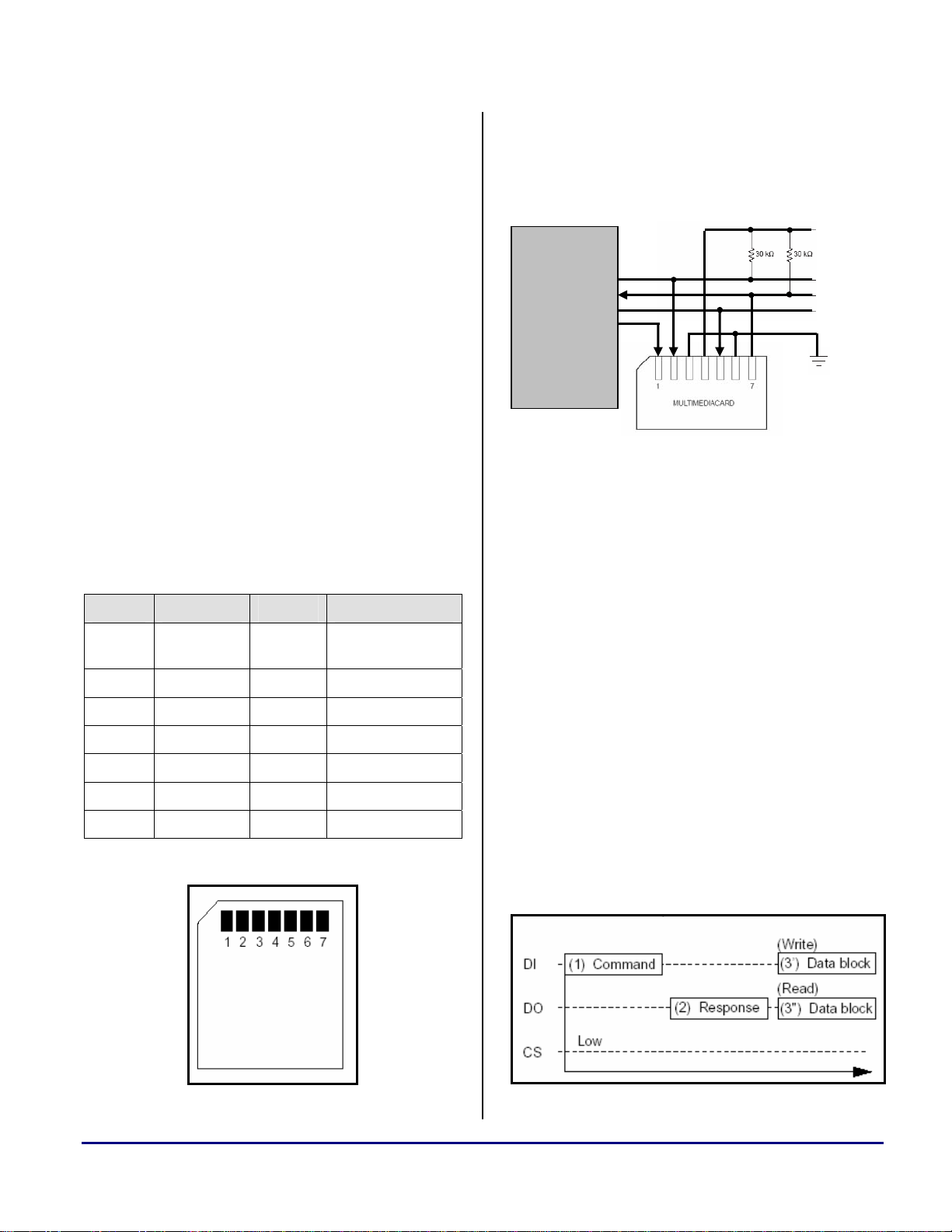
Pin Name Type Function
1 CS# Input Chip select
(active low)
2 Din Input Data input
3 VSS1 Power GND
4 VDD Power VCC
5 CLK Input Clock input
6 VSS2 Power GND
7 Dout Output Data output
Table 1. MultiMediaCard Pin Assignment
The MMC pin assignments in SPI mode are
shown in Table 1 and Figure 1. Figure 2 shows
the MMC interface with the ADSP-2126x SPI
port.
VCC
ADSP-2126x
SPI
MOSI
MISO
SPICLK
FLAGx
Figure 2. MultiMediaCard Interface with SPI Port
Din
Dout
CLK
GND
The MultiMediaCard Protocol
The SHARC processor's SPI issues commands to
the MMC over the data in (Din) pin of the MMC.
The data in pin of the MMC is connected to MOSI
of the SPI. The data is also written to the MMC
over the data in signal of the MMC. Based on the
received command, the MMC sends response or
data on the data out (Dout) pin. The data out pin
of the MMC is connected to MISO of the SHARC
processor's SPI port. The processor's SPI port
uses one of the Programmable Flag pins (FLAGx)
to drive CS# of the MMC. The communication is
initiated by different commands sent from the
SHARC processor to the MMC. All commands
are six bytes long and are transmitted MSB first.
Refer to Figure 3 for generic transfer protocol
between the MMC and the SHARC processor's
SPI port.
Figure 1. MultiMediaCard Pin Assignments
Interfacing MultiMediaCard™ with ADSP-2126x SHARC® Processors (EE-264) Page 2 of 6
Figure 3. MultiMediaCard Transfer Protocol
Page 3
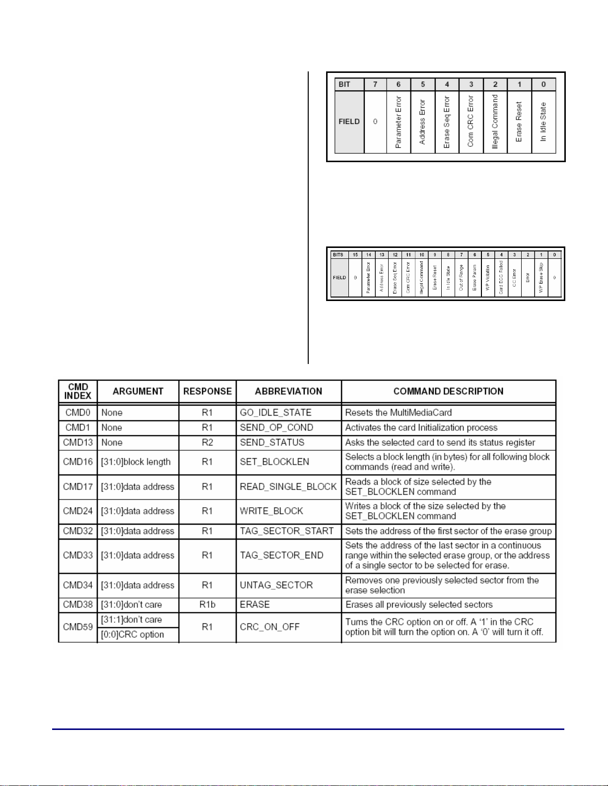
Commands and Responses
Table 2 lists the MultiMediaCard's most
commonly used commands in SPI mode. The
command format is shown in Figure 6.
Each MMC command consists of 48 bits (6
bytes) comprising a start bit (always 0), a transfer
bit (always 1), a 6-bit command field, a 4-byte
(32-bit) argument field, a 7-bit CRC field, and an
end bit (always 1). The argument field contains
the necessary information (card relative address,
read address, write address, etc.) for issuing that
command. For every received command (except
the SEND_STATUS command), the MMC responds
with a token value.
Figure 4. The MultiMediaCard R1 Response Format
Response format R2 is 2 bytes long. The response
token is sent by the card as a response to the
SEND_STATUS command. The format of the R2
status is shown in Figure 5.
a
The R1 response token is 1-byte long and its
MSB is always 0. The other bits in the response
indicate error conditions. The structure of an R1
response is shown in Figure 4. The R1 format
byte description is given in Table 3.
Figure 5. The MultiMediaCard R2 Response Format
The R2 format description is given in Table 4.
Table 2. Most Commonly Used MultiMediaCard Commands
Interfacing MultiMediaCard™ with ADSP-2126x SHARC® Processors (EE-264) Page 3 of 6
Page 4
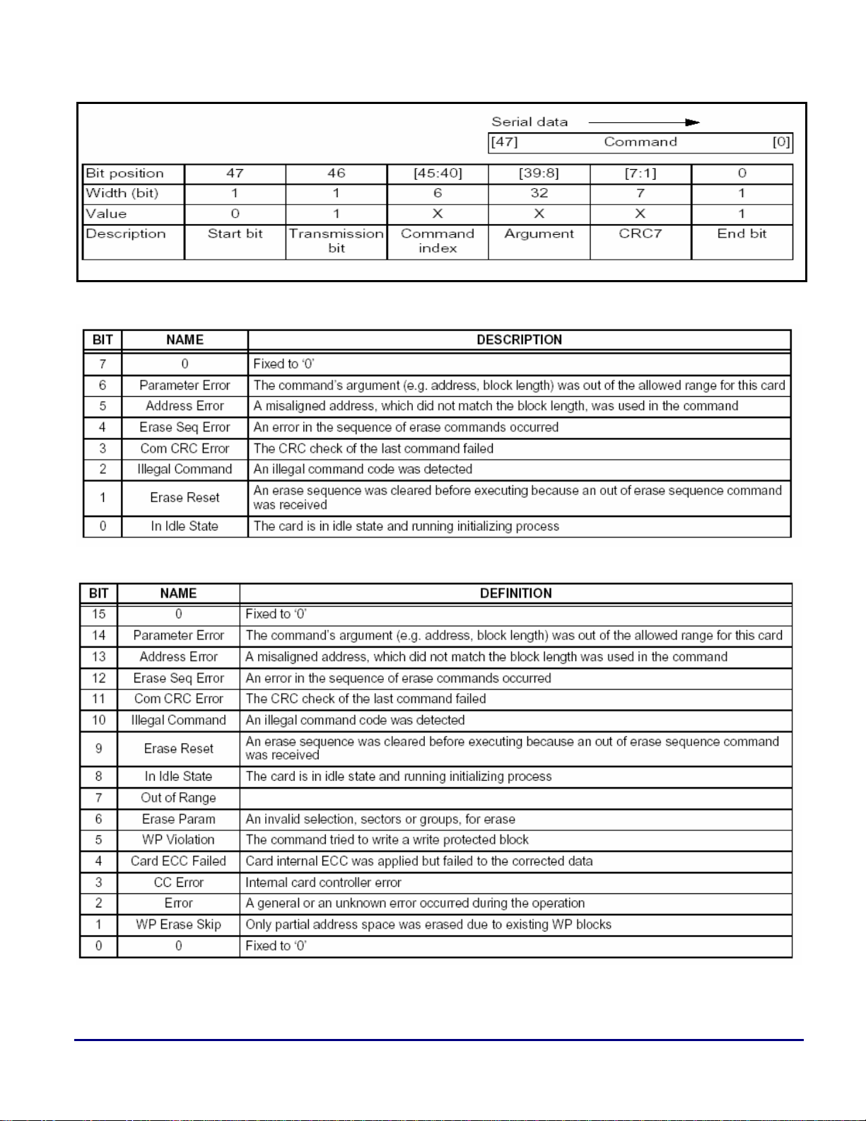
Figure 6. The MultiMediaCard Command Format
a
Table 3. MultiMediaCard R1 Response Format Description
Table 4. MultiMediaCard R2 Response Format Description
Interfacing MultiMediaCard™ with ADSP-2126x SHARC® Processors (EE-264) Page 4 of 6
Page 5
a
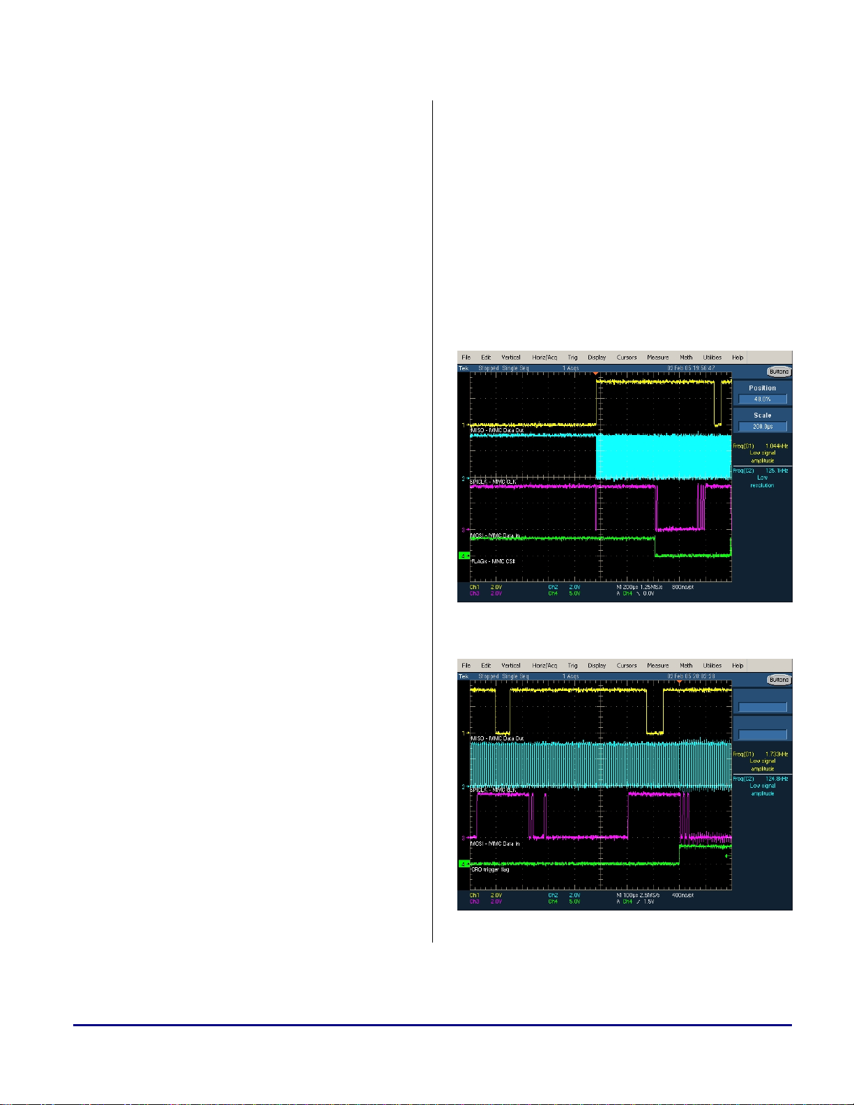
The Algorithm
By default, the MMC starts in MMC mode after
power up. To configure the card for SPI mode,
the CS# is driven logic low while transmitting the
CMD0 command. The following procedure is
required to set up data transfer in SPI mode.
1. After power up, drive CS# inactive (logic
high). This disables the card .
2. Issue at least 80 dummy clock cycles for
MMC initialization.
3. Drive CS# low and transmit a CMD0 command.
At this point, card mode changes from
default MMC mode to SPI mode.
4. Wait for an R1 response from the MMC. The
R1 response from the MMC should be 0x01.
Any other value indicates an error condition.
Re-execution starting from powering on may
be required.
MMC initialization
CMD0 (GO_IDLE_STATE)
CMD1 (SEND_OP_COND)
CMD16 (SET_BLOCKLEN)
CMD24 (WRITE_BLOCK)
CMD59 (CRC_ON_OFF)
CMD17 (READ_SINGLE_BLOCK)
The following are screen captures for some of
the MMC commands:
5. Issue a CMD1 command and wait for an R1
response. The R1 response should be 0x00.
Any other response value indicates of error
condition.
6. After a correct R1 response for CMD1, data
transfer can occur. Note that until the CMD1
command is successful, the SPI baud rate
(clock frequency) should be less than
400 kHz. Before data transfer can begin, the
SPI baud rate can be increased.
7. Commands such as set block length can now
be issued.
8. Issue commands to read/write the MMC
card.
9. When powering off, check that the card is in
the Ready state and drive
before turning off the power supplies.
The commands implemented in the supplied
code are:
CS# high (inactive)
Figure 7. Initialization with 80 CLK Cycles, CMD0
Command and R1 Response – 0x01
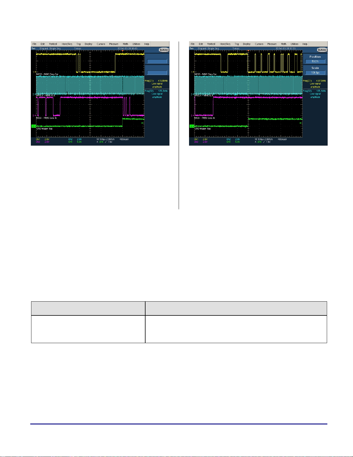
Figure 8. CMD1 Command and R1 Response - 0x00
Interfacing MultiMediaCard™ with ADSP-2126x SHARC® Processors (EE-264) Page 5 of 6
Page 6
a
Figure 9. Write Data Completed – 0x00 (BUSY)
Followed by 0xFF(High) Indicating Write Complete
Figure 10. Data Being Read After Receiving Read
Token 0xFE from the MMC
The example code is supplied in the file
EE264v01.zip associated with this EE-Note. For
further information on commands, responses, and
code flow, refer to the readme.txt file included
in the ZIP file.
References
[1] ADSP-2126x SHARC DSP Peripherals Manual. Rev 2.0, January 2004. Analog Devices, Inc.
[2] ADSP-21262 DSP EZ-KIT Lite Evaluation System Manual. Rev 1.2, March 2004, Analog Devices, Inc.
[3] Interfacing a MultiMediaCard to the LH79520 System-On-Chip. SHARP Application Note.
[4] MultiMediaCard User’s Manual, ADE-603-002B. Rev.3.0, 3/20/2003 Hitachi, Ltd.
Document History
Revision Description
Rev 1 – March 11, 2005
by Aseem Vasudev Prabhugaonkar
and Jagadeesh Rayala
Initial Release
Interfacing MultiMediaCard™ with ADSP-2126x SHARC® Processors (EE-264) Page 6 of 6
 Loading...