Analog Devices DAC08EP, DAC08CS-REEL, DAC08CS, DAC08HP, DAC08ES-REEL Datasheet
...
8-Bit, High-Speed, Multiplying D/A Converter
a
(Universal Digital Logic Interface)
FEATURES
Fast Settling Output Current: 85 ns
Full-Scale Current Prematched to ⴞ1 LSB
Direct Interface to TTL, CMOS, ECL, HTL, PMOS
Nonlinearity to 0.1% Maximum over
Temperature Range
High Output Impedance and Compliance:
–10 V to +18 V
Complementary Current Outputs
Wide Range Multiplying Capability: 1 MHz Bandwidth
Low FS Current Drift: ⴞ10 ppm/ⴗC
Wide Power Supply Range: ⴞ4.5 V to ⴞ18 V
Low Power Consumption: 33 mW @ ⴞ5 V
Low Cost
Available in Die Form
GENERAL DESCRIPTION
The DAC08 series of 8-bit monolithic digital-to-analog converters provide very high-speed performance coupled with low cost
and outstanding applications flexibility.
Advanced circuit design achieves 85 ns settling times with very
low “glitch” energy and at low power consumption. Monotonic
multiplying performance is attained over a wide 20-to-1 reference
current range. Matching to within 1 LSB between reference and
DAC08
full-scale currents eliminates the need for full-scale trimming in
most applications. Direct interface to all popular logic families
with full noise immunity is provided by the high swing, adjustable threshold logic input.
High voltage compliance complementary current outputs are
provided, increasing versatility and enabling differential operation to effectively double the peak-to-peak output swing. In
many applications, the outputs can be directly converted to
voltage without the need for an external op amp.
All DAC08 series models guarantee full 8-bit monotonicity,
and nonlinearities as tight as ± 0.1% over the entire operating
temperature range are available. Device performance is essentially unchanged over the ±4.5 V to ±18 V power supply range,
with 33 mW power consumption attainable at ±5 V supplies.
The compact size and low power consumption make the DAC08
attractive for portable and military/aerospace applications;
devices processed to MIL-STD-883, Level B are available.
DAC08 applications include 8-bit, 1 µs A/D converters, servo
motor and pen drivers, waveform generators, audio encoders
and attenuators, analog meter drivers, programmable power
supplies, CRT display drivers, high-speed modems and other
applications where low cost, high speed and complete input/
output versatility are required.
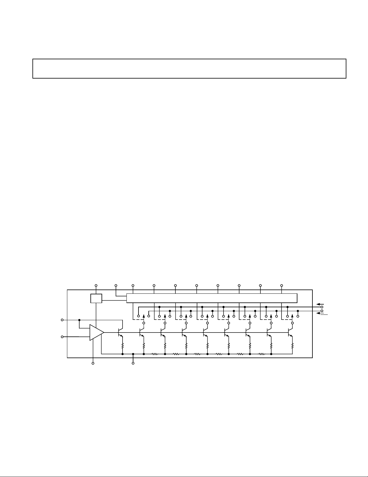
FUNCTIONAL BLOCK DIAGRAM
V+
13 1 5 6 7 8 9 10 11 12
DAC08
BIAS
NETWORK
14
V
(+)
REF
15
V
(–)
REF
REFERENCE
AMPLIFIER
16
COMP
V
LC
CURRENT
SWITCHES
MSB
B1
V–
B2 B3 B4 B5 B6 B7
3
REV. B
Information furnished by Analog Devices is believed to be accurate and
reliable. However, no responsibility is assumed by Analog Devices for its
use, nor for any infringements of patents or other rights of third parties that
may result from its use. No license is granted by implication or otherwise
under any patent or patent rights of Analog Devices.
LSB
B8
I
OUT
4
2
I
OUT
One Technology Way, P.O. Box 9106, Norwood, MA 02062-9106, U.S.A.
Tel: 781/329-4700 www.analog.com
Fax: 781/326-8703 © Analog Devices, Inc., 2002

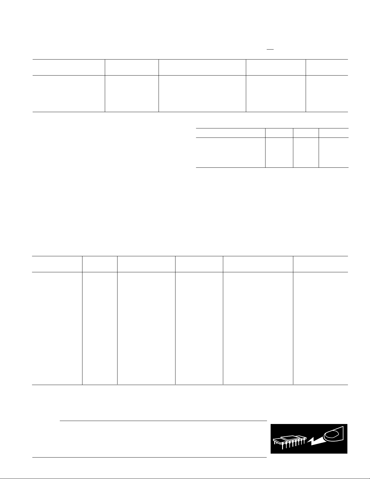
DAC08–SPECIFICATIONS
ELECTRICAL CHARACTERISTICS
for DAC08E and DAC08H, –40ⴗC to +85ⴗC for DAC08C, unless otherwise noted. Output characteristics refer to both I
(@ VS = ⴞ15 V, I
= 2.0 mA, –55ⴗC TA +125ⴗC for DAC08/08A, 0ⴗC TA +70ⴗC
REF
OUT
and
I
.)
OUT
DAC08A/H DAC08E DAC08C
Parameter Symbol Conditions Min Typ Max Min Typ Max Min Typ Max Unit
Resolution 8 8 8 Bits
Monotonicity 8 8 8 Bits
Nonlinearity NL ± 0.1 ± 0.19 ± 0.39 % FS
Settling Time t
Propagation Delay
Each Bit t
All Bits Switched t
Full-Scale Tempco
1
S
PLH
PHL
TCI
To ± 1/2 LSB, 85 135 85 150 85 150 ns
All Bits Switched ON
or OFF, T
TA = 25°C
= 25°C
A
1
1
35 60 35 60 35 60 ns
35 60 35 60 35 60 ns
FS
± 10 ± 50 ± 10 ± 80 ±10 ± 80 ppm/°C
DAC08E ± 50
Output Voltage
Compliance V
Full-Scale Current
OC
(True Compliance) Change <1/2 LSB, –10 +18 –10 +18 –10 +18 V
R
> 20 MΩ typ
Full Range Current I
FR4
OUT
V
= 10.000 V 1.984 1.992 2.000 1.94 1.99 2.04 1.94 1.99 2.04 mA
REF
R14, R15 = 5.000 kΩ
T
= 25°C
Full Range Symmetry I
Zero-Scale Current I
Output Current Range I
I
FRS
ZS
OR1
OR2
A
I
FR4
– I
FR2
± 0.5 ± 4 ± 1 ± 8 ±2 ± 16 µA
0.1 1 0.2 2 0.2 4 µA
R14, R15 = 5.000 kΩ 2.1 2.1 2.1 mA
V
= +15.0 V,
REF
V– = –10 V
V
= +25.0 V, 4.2 4.2 4.2 mA
REF
V– = –12 V
Output Current Noise I
= 2 mA 25 25 25 nA
REF
Logic Input Levels
Logic “0” V
Logic Input “1” V
Logic Input Current V
Logic “0” I
Logic Input “1” I
IL
IH
Logic Input Swing V
Logic Threshold Range V
Reference Bias Current I
15
Reference Input dI/dt R
Slew Rate R
Power Supply Sensitivity PSSI
PSSI
Power Supply Current I+ VS = ± 5 V, I
VLC = 0 V 0.8 0.8 0.8 V
IL
IL
LC
= 0 V
22 2 V
VIN = –10 V to +0.8 V –2 –10 –2 –10 –2 –10 µA
VIN = 2.0 V to 18 V 0.002 10 0.002 10 0.002 10 µA
V– = –15 V –10 +18 –10 +18 –10 +18 V
IS
THR
VS = ± 15 V
1
–10 +13.5 –10 +13.5 –10 +13.5 V
–1 –3 –1 –3 –1 –3 µA
= 200 Ω 4 8 4 8 4 8 mA/µs
EQ
= 100 Ω
L
C
= 0 pF See Fast Pulsed Ref. Info Following.
C
V+ = 4.5 V to 18 V ± 0.0003 ± 0.01 ± 0.0003 ± 0.01 ± 0.0003 ± 0.01 %∆IO/%∆V+
FS+
V– = –4.5 V to –18 V ± 0.002 ± 0.01 ± 0.002 ±0.01 ± 0.002 ± 0.01 %∆IO/%∆V–
FS–
I
= 1.0 mA
REF
= 1.0 mA 2.3 3.8 2.3 3.8 2.3 3.8 mA
REF
1
I– –4.3 –5.8 –4.3 –5.8 –4.3 –5.8 mA
Power Dissipation P
I+ V
I– I
I+ V
I– I
D
= +5 V, –15 V, 2.4 3.8 2.4 3.8 2.4 3.8 mA
S
= 2.0 mA –6.4 –7.8 –6.4 –7.8 –6.4 –7.8 mA
REF
= ±15 V, 2.5 3.8 2.5 3.8 2.5 3.8 mA
S
= 2.0 mA –6.5 –7.8 –6.5 –7.8 –6.5 –7.8 mA
REF
± 5 V, I
= 1.0 mA 33 48 33 48 33 48 mW
REF
+5 V, –15 V,
I
= 2.0 mA 108 136 103 136 108 136 mW
REF
± 15 V, I
NOTES
1
Guaranteed by design.
Specifications subject to change without notice.
= 2.0 mA 135 174 135 174 135 174 mW
REF
–2–
REV. B

DAC08
WARNING!
ESD SENSITIVE DEVICE
TYPICAL ELECTRICAL CHARACTERISTICS
(@ VS = ⴞ15 V, and I
characteristics apply to both I
= 2.0 mA, unless otherwise noted. Output
REF
OUT
and
I
.)
OUT
All Grades
Parameter Symbol Conditions Typical Unit
Reference Input Slew Rate dI/dt 8 mA/µs
Propagation Delay t
Settling Time t
PLH
S
, t
PHL
TA = 25°C, Any Bit 35 ns
To ± 1/2 LSB, All Bits
Switched ON or OFF, 85 ns
TA = 25°C
Specifications subject to change without notice.
ABSOLUTE MAXIMUM RATINGS
1
Operating Temperature
DAC08AQ, Q . . . . . . . . . . . . . . . . . . . . . –55°C to +125°C
DAC08HQ, EQ, CQ, HP, EP . . . . . . . . . . . . 0°C to +70°C
DAC08CP, CS . . . . . . . . . . . . . . . . . . . . . –40°C to +85°C
Junction Temperature (T
) . . . . . . . . . . . . . –65°C to +150°C
J
Storage Temperature Q Package . . . . . . . . . –65°C to +150°C
Storage Temperature P Package . . . . . . . . . –65°C to +125°C
Lead Temperature (Soldering, 60 sec) . . . . . . . . . . . . . 300°C
V+ Supply to V– Supply . . . . . . . . . . . . . . . . . . . . . . . . . 36 V
Logic Inputs . . . . . . . . . . . . . . . . . . . . . . . V– to V– plus 36 V
. . . . . . . . . . . . . . . . . . . . . . . . . . . . . . . . . . . . . . V– to V+
V
LC
Analog Current Outputs (at V
Reference Input (V
to V15) . . . . . . . . . . . . . . . . . . . V– to V+
14
– = 15 V) . . . . . . . . . . 4.25 mA
S
Package Type
16-Lead Cerdip (Q) 100 16 °C/W
16-Lead Plastic DIP (P) 82 39 °C/W
20-Terminal LCC (RC) 76 36 °C/W
16-Lead SO (S) 111 35 °C/W
NOTES
1
Absolute maximum ratings apply to both DICE and packaged parts, unless
otherwise noted.
2
θJA is specified for worst-case mounting conditions, i.e., θJA is specified for device
in socket for cerdip, Plastic DIP, and LCC packages; θJA is specified for device
soldered to printed circuit board for SO package.
2
JA
JC
Unit
Reference Input Differential Voltage
to V15) . . . . . . . . . . . . . . . . . . . . . . . . . . . . . . . . ± 18 V
(V
14
Reference Input Current (I
) . . . . . . . . . . . . . . . . . . . 5.0 mA
14
ORDERING GUIDE
1
Temperature Package Package # Parts Per
Model NL Range Description Option Container
DAC08AQ ± 0.10% –55°C to +125°C Cerdip-16 Q-16 25
DAC08AQ
2
/883C ±0.10% –55°C to +125°C Cerdip-16 Q-16 25
DAC08HP ± 0.10% 0°C to 70°C P-DIP-16 N-16 25
DAC08HQ ± 0.10% 0°C to 70°C Cerdip-16 Q-16 25
DAC08Q ± 0.19% –55°C to +125°C Cerdip-16 Q-16 25
DAC08Q
2
/883C ± 0.19% –55°C to +125°C Cerdip-16 Q-16 25
DAC08RC/883C ± 0.19% –55°C to +125°C LCC-20 E-20 55
DAC08EP ± 0.19% 0°C to 70°C P-DIP-16 N-16 25
DAC08EQ ± 0.19% 0°C to 70°C Cerdip-16 Q-16 25
DAC08ES ±0.19% 0°C to 70°C SO-16 R-16A (Narrow Body) 47
DAC08ES-REEL ±0.19% 0°C to 70° C SO-16 R-16A (Narrow Body) 2500
DAC08CP ± 0.39% –40°C to +85°C P-DIP-16 N-16 25
DAC08CQ ± 0.39% 0°C to 70°C Cerdip-16 Q-16 25
DAC08CS ± 0.39% –40°C to +85°C SO-16 R-16A (Narrow Body) 47
DAC08CS-REEL ± 0.39% –40°C to +85°C SO-16 R-16A (Narrow Body) 2500
DAC08NBC ± 0.10% 25°C DICE
DAC08GBC ± 0.19% 25°C DICE
DAC08GRBC ± 0.39% 25°C DICE
NOTES
1
Devices processed in total compliance to MIL-STD-883. Consult factory for 883 data sheet.
2
For availability and burn-in information on SO and PLCC packages, contact your local sales office.
The DAC08 contains 84 transistors. Die size 63 mil x 87 mil = 5,481 square mils.
CAUTION
ESD (electrostatic discharge) sensitive device. Electrostatic charges as high as 4000 V readily
accumulate on the human body and test equipment and can discharge without detection. Although
the DAC08 features proprietary ESD protection circuitry, permanent damage may occur on devices
subjected to high-energy electrostatic discharges. Therefore, proper ESD precautions are
recommended to avoid performance degradation or loss of functionality.
REV. B
–3–

DAC08
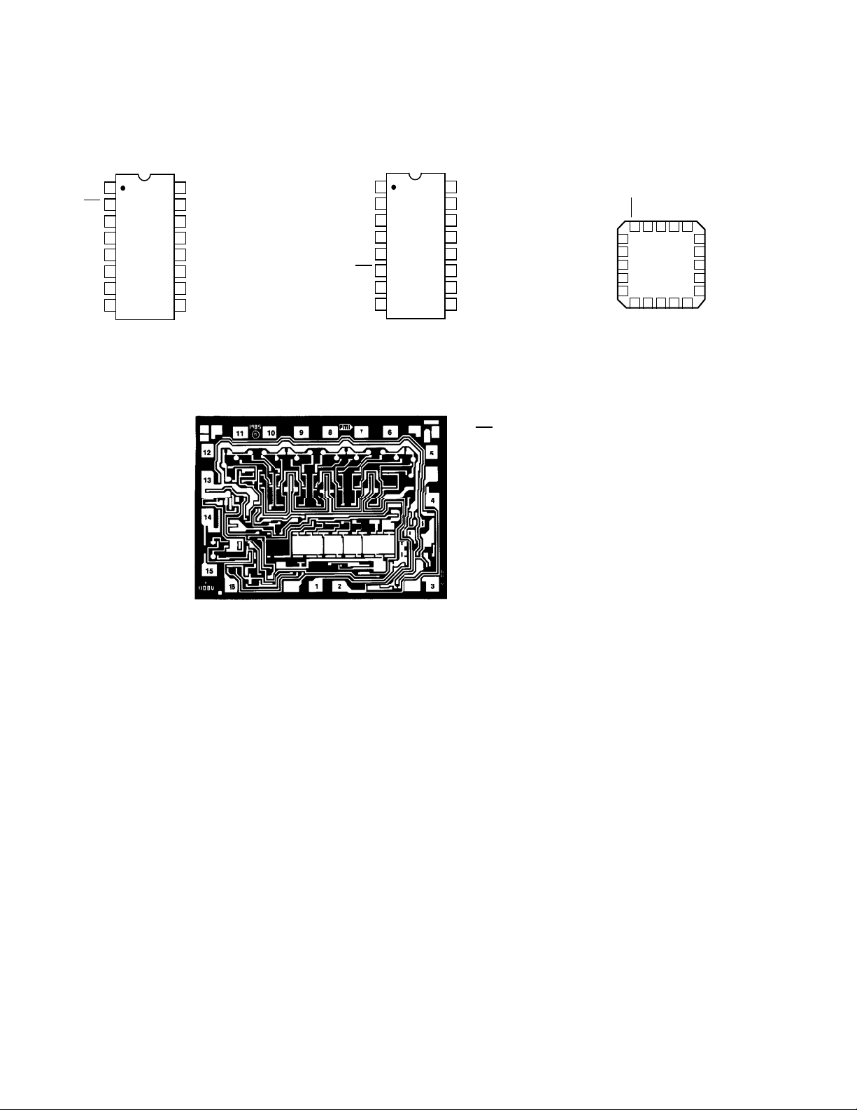
PIN CONNECTIONS
16-Lead Dual-In-Line Package
(Q and P Suffix)
V
I
OUT
I
OUT
MSB B1
1
LC
2
3
V–
4
5
6
B2
7
B3
8
B4
16
COMPENSATION
15
V
(–)
REF
14
V
(+)
REF
13
V+
12
B8 LSB
11
B7
10
B6
9
B5
16-Lead SO
(S Suffix)
16
15
14
13
12
11
10
9
B8 LSB
B7
B6
B5
B4
B3
B2
B1 MSB
V
REF
V
REF
(+)
(–)
COMP
V
I
OUT
I
OUT
1
V+
2
3
4
5
LC
6
7
V–
8
DICE CHARACTERISTICS
(125°C Tested Dice Available)
1. V
LC
2. I
OUT
3. V–
4. I
OUT
5. BIT 1 (MSB)
6. BIT 2
7. BIT 3
8. BIT 4
9. BIT 5
10. BIT 6
11. BIT 7
12. BIT 8 (LSB)
13. V+
(+)
14. V
REF
15. V
(–)
REF
16. COMP
DIE SIZE 0.087 ⴛ 0.063 inch, 5,270 sq. mils
(2.209 ⴛ 1.60 mm, 3.54 sq. mm)
DAC08RC/883 20-Lead LCC
(RC Suffix)
(–)
LC
NC
V
20 19123
B4NCB5
V
COMP
B6
REF
18
17
16
15
14
V
REF
V+
NC
B8 LSB
B7
(+)
I
OUT
NC
MSB B1
V–
B2
OUT
I
4
5
6
7
8
10 11 12 13
9
B3
NC = NO CONNECT
–4–
REV. B
 Loading...