ANALOG DEVICES DAC08 Service Manual
8-Bit, High Speed, Multiplying D/A Converter
FEATURES
Fast settling output current: 85 ns
Full-scale current prematched to ±1 LSB
Direct interface to TTL, CMOS, ECL, HTL, PMOS
Nonlinearity to 0.1% maximum over temperature range
High output impedance and compliance: −10 V to +18 V
Complementary current outputs
Wide range multiplying capability: 1 MHz bandwidth
Low FS current drift: ±10 ppm/°C
Wide power supply range: ±4.5 V to ±18 V
Low power consumption: 33 mW @ ±5 V
Low cost
GENERAL DESCRIPTION
The DAC08 series of 8-bit monolithic digital-to-analog converters provide very high speed performance coupled with low cost
and outstanding applications flexibility.
Advanced circuit design achieves 85 ns settling times with very
low “glitch” energy and at low power consumption. Monotonic
multiplying performance is attained over a wide 20-to-1
reference current range. Matching to within 1 LSB between
reference and full-scale currents eliminates the need for full-
(Universal Digital Logic Interface)
DAC08
scale trimming in most applications. Direct interface to all
popular logic families with full noise immunity is provided by
the high swing, adjustable threshold logic input.
High voltage compliance complementary current outputs are
provided, increasing versatility and enabling differential
operation to effectively double the peak-to-peak output swing.
In many applications, the outputs can be directly converted to
voltage without the need for an external op amp. All DAC08
series models guarantee full 8-bit monotonicity, and nonlinearities as tight as ±0.1% over the entire operating temperature
range are available. Device performance is essentially unchanged
over the ±4.5 V to ±18 V power supply range, with 33 mW
power consumption attainable at ±5 V supplies.
The compact size and low power consumption make the DAC08
attractive for portable and military/aerospace applications;
devices processed to MIL-STD-883, Level B are available.
DAC08 applications include 8-bit, 1 µs A/D converters, servo
motor and pen drivers, waveform generators, audio encoders
and attenuators, analog meter drivers, programmable power
supplies, LCD display drivers, high speed modems, and other
applications where low cost, high speed, and complete
input/output versatility are required.
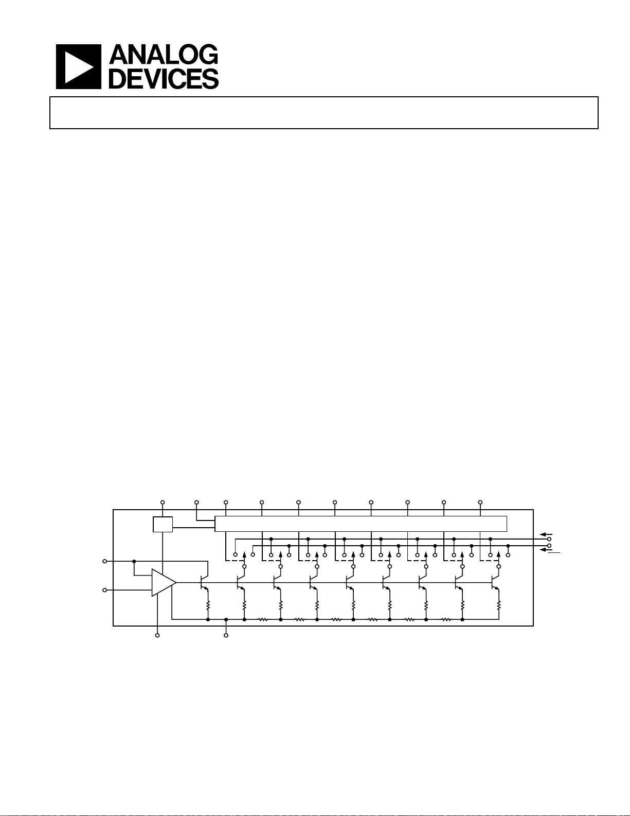
FUNCTIONAL BLOCK DIAGRAM
V+ V
13 1 5 6 7 8 9 10 11 12
DAC08
BIAS
NETWORK
14
V
(+)
REF
15
V
(–)
REF
REFERENCE
AMPLIFIER
Rev. C
Information furnished by Analog Devices is believed to be accurate and reliable.
However, no responsibility is assumed by Analog Devices for its use, nor for any
infringements of patents or other rights of third parties that may result from its use.
Specifications subject to change without notice. No license is granted by implication
or otherwise under any patent or patent rights of Analog Devices. Trademarks and
registered trademarks are the property of their respective owners.
LC
CURRENT
SWITCHES
(MSB)
B1
V–COMP
B2 B3 B4 B5 B6 B7
316
Figure 1.
(LSB)
B8
I
OUT
4
2
I
OUT
00268-C-001
One Technology Way, P.O. Box 9106, Norwood, MA 02062-9106, U.S.A.
Tel: 781.329.4700
Fax: 781.326.8703 © 2004 Analog Devices, Inc. All rights reserved.
www.analog.com

DAC08
TABLE OF CONTENTS
Specifications..................................................................................... 3
Electrical Characteristics............................................................. 3
Typical E l e ctric a l Characte r i s tics ............................................... 4
Absolute Maximum Ratings............................................................ 5
ESD Caution.................................................................................. 5
Pin Connections ............................................................................... 6
Test and Burn-In Circuits................................................................ 7
Typical Performance Characteristics ............................................. 8
Basic Connections.......................................................................... 11
Application Information................................................................ 13
Reference Amplifier Setup ........................................................ 13
Reference Amplifier Compensation for Multiplying
Applications
Logic Inputs................................................................................. 13
Analog Output Currents ........................................................... 14
Power Supplies ............................................................................ 14
Temperature Performance......................................................... 14
Multiplying Operation............................................................... 14
Settling Time............................................................................... 14
ADI Current Output DACs........................................................... 16
Outline Dimensions ....................................................................... 17
Ordering Guide .......................................................................... 18
................................................................................ 13
REVISION HISTORY
11/04—Rev. B to Rev. C
Changed SO to SOIC .........................................................Universal
Removed DIE......................................................................Universal
Changes to Figure 30, Figure 31, Figure 32................................. 12
Change to Figure 33 ....................................................................... 15
Added Table 4.................................................................................. 16
Updated Outline Dimensions....................................................... 17
Changes to Ordering Guide.......................................................... 18
2/02—Rev. A to Rev. B
Edits to SPECIFICATIONS............................................................. 2
Edits to ABSOLUTE MAXIMUM RATING ................................ 3
Edits to ORDERING GUIDE.......................................................... 3
Edits to WAFER TEST LIMITS...................................................... 5
Edit to Figure 13 ............................................................................... 8
Edits to Figures 14 and 15 ............................................................... 9
Rev. C | Page 2 of 20

DAC08
SPECIFICATIONS
ELECTRICAL CHARACTERISTICS
VS = ±15 V, I
DAC08C, unless otherwise noted. Output characteristics refer to both I
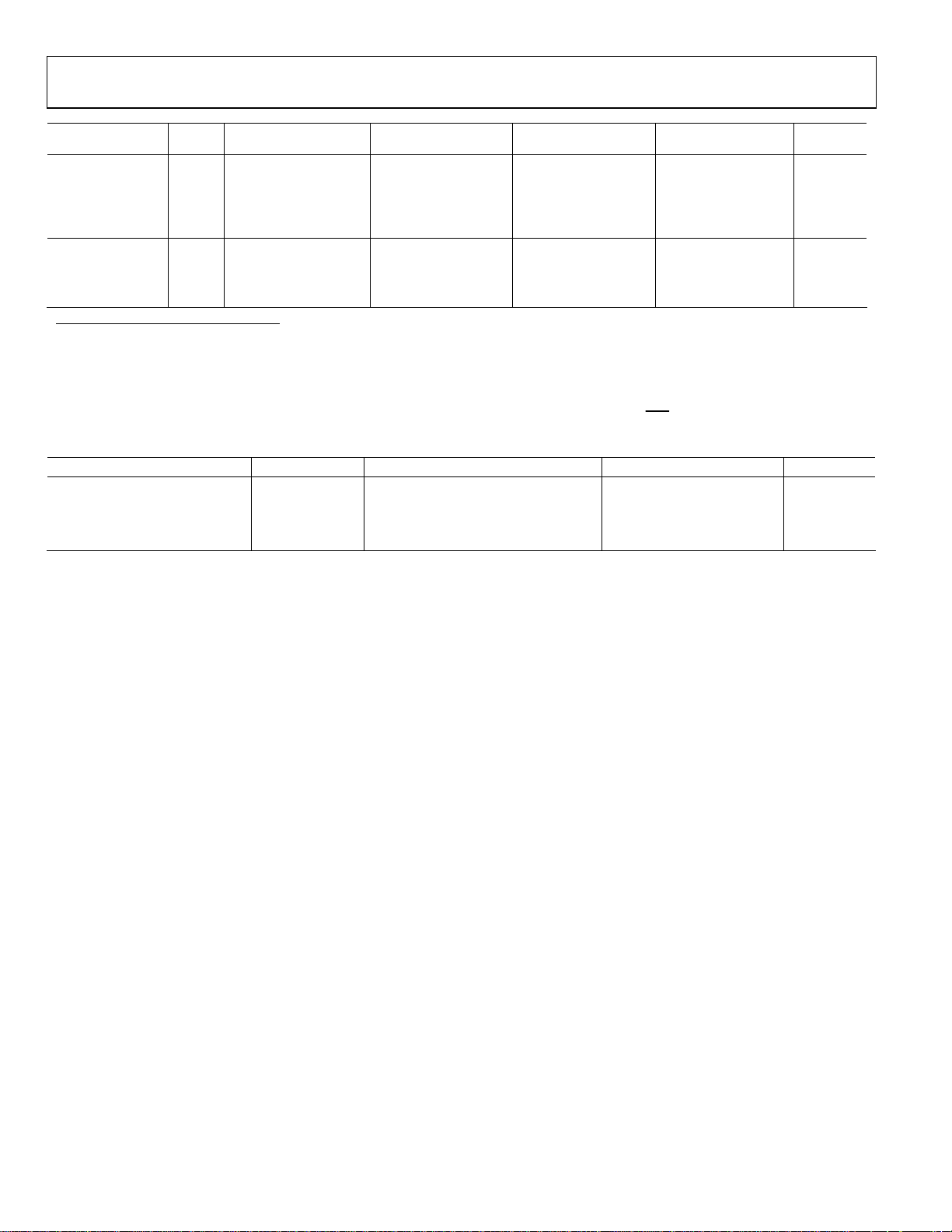
Table 1.
DAC08A/DAC08H DAC08E DAC08C
Parameter
Resolution 8 8 8 Bits
Monotonicity 8 8 8 Bits
Nonlinearity NL ±0.1 ±0.19 ±0.39 %FS
Settling Time t
Propagation Delay
Each Bit t
All Bits Switched t
Full-Scale Tempco1 TCI
DAC08E ±50
Output Voltage
Compliance V
(True Compliance) Change <1/2 LSB, R
Full Range Current I
Full Range Symmetry I
Zero-Scale Current I
Output Current
Range
I
V
V− = −12 V
Output Current
Noise
Logic Input Levels
Logic 0 V
Logic 1 V
Logic Input Current VLC = 0 V
Logic 0 I
Logic 1 I
Logic Input Swing V
Logic Threshold
Range
Reference Bias
Current
Reference Input dI/dt REQ = 200 Ω 4 8 4 8 4 8 mA/µs
Slew Rate RL = 100 Ω
C
Power Supply
Sensitivity
PSSI
I
= 2.0 mA, –55°C ≤ TA ≤ +125°C for DAC08/DAC08A, 0°C ≤ TA ≤ +70°C for DAC08E and DAC08H, −40°C to +85°C for
REF
I
OUT
Symbol
S
PLH
PHL
FS
OC
and
OUT
Conditions Min Typ Max Min Typ Max Min Typ Max Unit
To ±1/2 LSB, all bits
switched on or off,
1
= 25°C
T
A
85 135 85 150 85 150 ns
TA = 25°C1 35 60 35 60 35 60 ns
35 60 35 60 35 60 ns
±10 ±50 ±10 ±80 ±10 ±80 ppm/°C
Full-scale current
>
OUT
−10 +18 −10 +18 –10 +18 V
.
20 MΩ typ
V
FR4
FRS
ZS
I
OR1
OR2
= 10.000 V R14, R15 =
REF
5.000 kΩ T
I
FR4
− I
= 25°C
A
FR2
0.1 1 0.2 2 0.2 4 µA
R14, R15 = 5.000 kΩ 2.1 2.1 2.1 mA
V
= +15.0 V,
REF
1.984 1.992 2.000 1.94 1.99 2.04 1.94 1.99 2.04 mA
±0.5 ±4 ±1 ±8 ±2 ±16 µA
V− = −10 V
= +25.0 V, 4.2 4.2 4.2 mA
REF
I
IL
IL
IL
IH
IS
V
THR
I
15
PSSI
FS+
FS–
= 2 mA 25 25 25 nA
REF
VLC = 0 V 0.8 0.8 0.8 V
2 2 2 V
VIN = −10 V to +0.8 V −2 −10 −2 −10 −2 −10 µA
VIN = 2.0 V to 18 V 0.002 10 0.002 10 0.002 10 µA
V− = −15 V −10 +18 −10 +18 −10 +18 V
VS = ±15 V1 −10 +13.5 −10 +13.5 −10 +13.5 V
−1 −3 −1 −3 −1 −3 µA
= 0 pF. See Figure 7.
C
1
V+ = 4.5 V to 18 V ±0.0003 ±0.01 ±0.0003 ±0.01 ±0.0003 ±0.01 %∆IO/%∆V+
V− = −4.5 V to −18 V ±0.002 ±0.01 ±0.002 ±0.01 ±0.002 ±0.01 %∆IO/%∆V−
= 1.0 mA
REF
Rev. C | Page 3 of 20
DAC08
DAC08A/DAC08H DAC08E DAC08C
Parameter
Power Supply Current I+ VS = ±5 V, I
I− −4.3 −5.8 −4.3 −5.8 −4.3 −5.8 mA
I+ VS = +5 V, −15 V, 2.4 3.8 2.4 3.8 2.4 3.8 mA
I− I
I+ VS = ±15 V, 2.5 3.8 2.5 3.8 2.5 3.8 mA
I− I
Power Dissipation P
I
135 174 135 174 135 174 mW
1
Guaranteed by design.
TYPICAL ELECTRICAL CHARACTERISTICS
VS = ±15 V, and I
Table 2.
Parameter Symbol Conditions All Grades Typical Unit
Reference Input Slew Rate dI/dt 8 mA/µs
Propagation Delay t
Settling Time t
Symbol
D
= 2.0 mA, unless otherwise noted. Output characteristics apply to both I
REF
Conditions Min Typ Max Min Typ Max Min Typ Max Unit
= 1.0 mA 2.3 3.8 2.3 3.8 2.3 3.8 mA
REF
= 2.0 mA −6.4 −7.8 −6.4 −7.8 −6.4 −7.8 mA
REF
= 2.0 mA −6.5 −7.8 −6.5 −7.8 −6.5 −7.8 mA
REF
±5 V, I
= 1.0 mA +5 V,
REF
−15 V,
= 2.0 mA ±15 V, I
REF
2.0 mA
, t
PLH
PHL
S
REF
33 48 33 48 33 48 mW
=
108 136 103 136 108 136 mW
TA = 25°C, any bit 35 ns
To ±1/2 LSB, all bits switched on or
= 25°C
off, T
A
OUT
and
.
I
OUT
85 ns
Rev. C | Page 4 of 20
DAC08
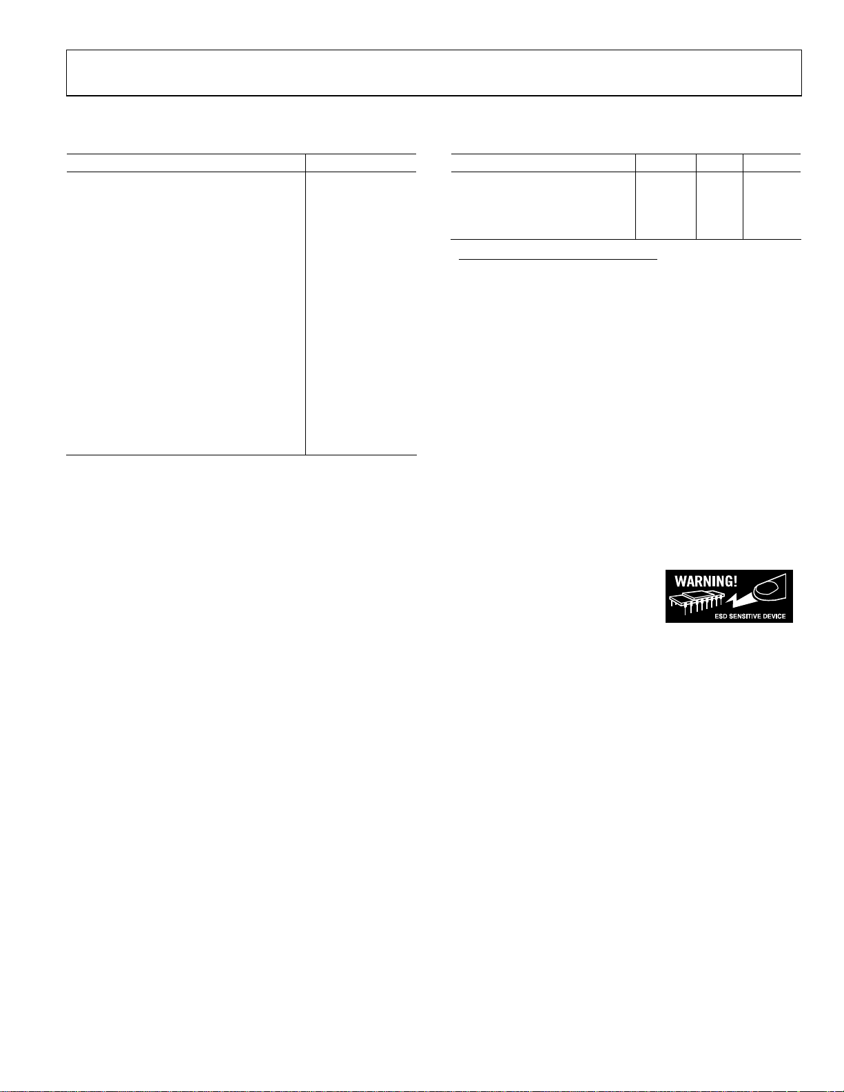
ABSOLUTE MAXIMUM RATINGS
Table 3.
Parameter Rating
Operating Temperature
DAC08AQ, DAC08Q −55°C to +125°C
DAC08HQ, DAC08EQ, DAC08CQ,
0°C to +70°C
DAC08HP, DAC08EP
DAC08CP, DAC08CS −40°C to +85°C
Junction Temperature (TJ) −65°C to +150°C
Storage Temperature Q Package −65°C to +150°C
Storage Temperature P Package −65°C to +125°C
Lead Temperature (Soldering, 60 sec) 300°C
V+ Supply to V− Supply 36 V
Logic Inputs V− to V− + 36 V
V
LC
V− to V+
Analog Current Outputs (at VS− = 15 V) 4.25 mA
Reference Input (V
to V15) V− to V+
14
Reference Input Differential Voltage
(V14 to V15) ±18 V
Reference Input Current (I14) 5.0 mA
Package Type θ
1
JA
θ
Unit
JC
16-Lead CERDIP (Q) 100 16 °C/W
16-Lead PDIP (P) 82 39 °C/W
20-Terminal LCC (RC) 76 36 °C/W
16-Lead SOIC (S) 111 35 °C/W
1
θJA is specified for worst-case mounting conditions, that is, θJA is specified for
device in socket for CERDIP, PDIP, and LCC packages; θ
device soldered to printed circuit board for SOIC package.
is specified for
JA
Stresses greater than those listed under Absolute Maximum
Ratings may cause permanent damage to the device. This is a
stress rating only and functional operation of the device at these
or any other conditions above those indicated in the operational
section of this specification is not implied. Exposure to absolute
maximum rating conditions for extended periods may affect
device reliability.
ESD CAUTION
ESD (electrostatic discharge) sensitive device. Electrostatic charges as high as 4000 V readily accumulate on
the human body and test equipment and can discharge without detection. Although this product features
proprietary ESD protection circuitry, permanent damage may occur on devices subjected to high energy
electrostatic discharges. Therefore, proper ESD precautions are recommended to avoid performance
degradation or loss of functionality.
Rev. C | Page 5 of 20
DAC08
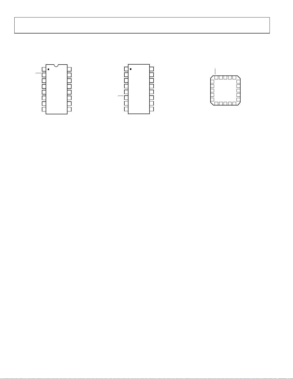
PIN CONNECTIONS
1
V
LC
I
2
OUT
V–
3
OUT
B2
B3
B4
DAC08
4
TOP VIEW
(Not To Scale)
5
6
7
8
I
(MSB) B1
Figure 2. 16-Lead Dual In-Line Package
(Q and P Suffixes)
16
COMP
V
15
V
14
V+
13
12
B8 (LSB)
B7
11
10
B6
9
B5
REF
REF
(–)
(+)
00268-C-002
V
REF
V
REF
COMP
I
I
(+)
(–)
V
OUT
OUT
V+
LC
V–
1
2
3
DAC08
4
TOP VIEW
(Not To Scale)
5
6
7
8
16
B8 (LSB)
B7
15
B6
14
B5
13
12
B4
B3
11
10
B2
9
B1 (MSB)
00268-C-003
Figure 3. 16-Lead SOIC
(S Suffix)
(–)
LC
REF
V
NC
V
COMP
20 19123
V
18
REF
V+
17
NC
16
15
B8 (LSB)
B7
14
B5
B6
B4
NC
I
OUT
NC
(MSB) B1
OUT
I
4
V–
5
DAC08
TOP VIEW
6
(Not To Scale)
7
B2
8
10 11 12 13
9
B3
NC = NO CONNECT
Figure 4. DAC08RC/883 20-Lead LCC
(RC Suffix)
(+)
00268-C-004
Rev. C | Page 6 of 20
 Loading...