REV. B
Information furnished by Analog Devices is believed to be accurate and
reliable. However, no responsibility is assumed by Analog Devices for its
use, nor for any infringements of patents or other rights of third parties
which may result from its use. No license is granted by implication or
otherwise under any patent or patent rights of Analog Devices.
a
AD807
One Technology Way, P.O. Box 9106, Norwood, MA 02062-9106, U.S.A.
Tel: 781/329-4700 World Wide Web Site: http://www.analog.com
Fax: 781/326-8703 © Analog Devices, Inc., 2000
Fiber Optic Receiver with Quantizer and
Clock Recovery and Data Retiming
FEATURES
Meets CCITT G.958 Requirements
for STM-1 Regenerator—Type A
Meets Bellcore TR-NWT-000253 Requirements for OC-3
Output Jitter: 2.0 Degrees RMS
155 Mbps Clock Recovery and Data Retiming
Accepts NRZ Data, No Preamble Required
Phase-Locked Loop Type Clock Recovery—
No Crystal Required
Quantizer Sensitivity: 2 mV
Level Detect Range: 2.0 mV to 30 mV
Single Supply Operation: +5 V or –5.2 V
Low Power: 170 mW
10 KH ECL/PECL Compatible Output
Package: 16-Lead Narrow 150 mil SOIC
reliance on external components such as a crystal or a SAW
filter, to aid frequency acquisition.
The AD807 acquires frequency and phase lock on input data
using two control loops that work without requiring external
control. The frequency acquisition control loop initially acquires
the frequency of the input data, acquiring frequency lock on
random or scrambled data without the need for a preamble. At
frequency lock, the frequency error is zero and the frequency
detector has no further effect. The phase acquisition control
loop then works to ensure that the output phase tracks the input
phase. A patented phase detector has virtually eliminated pattern
jitter throughout the AD807.
The device VCO uses a ring oscillator architecture and patented
low noise design techniques. Jitter is 2.0 degrees rms. This low
jitter results from using a fully differential signal architecture,
Power Supply Rejection Ratio circuitry and a dielectrically
isolated process that provides immunity from extraneous signals
on the IC. The device can withstand hundreds of millivolts of
power supply noise without an effect on jitter performance.
The user sets the jitter peaking and acquisition time of the PLL
by choosing a damping factor capacitor whose value determines
loop damping. CCITT G.958 Type A jitter transfer requirements can easily be met with a damping factor of 5 or greater.
Device design guarantees that the clock output frequency will
drift by less than 20% in the absence of input data transitions.
Shorting the damping factor capacitor, C
D
, brings the clock
output frequency to the VCO center frequency.
The AD807 consumes 170 mW and operates from a single
power supply at either +5 V or –5.2 V.
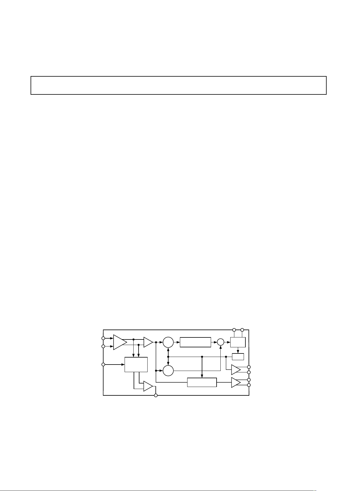
FUNCTIONAL BLOCK DIAGRAM
COMPENSATING
ZERO
LOOP
FILTER
SIGNAL
LEVEL
DETECTOR
VCO
⌽
DET
+
–
+
–
F
DET
⌺
RETIMING
DEVICE
PHASE-LOCKED LOOP
AD807
LEVEL
DETECT
COMPARATOR/
BUFFER
QUANTIZER
PIN
NIN
THRADJ
SDOUT
CLKOUTP
CLKOUTN
DATAOUTP
DATAOUTN
CF1 CF2
PRODUCT DESCRIPTION
The AD807 provides the receiver functions of data quantization,
signal level detect, clock recovery and data retiming for 155 Mbps
NRZ data. The device, together with a PIN diode/preamplifier
combination, can be used for a highly integrated, low cost, low
power SONET OC-3 or SDH STM-1 fiber optic receiver.
The receiver front end signal level detect circuit indicates when
the input signal level has fallen below a user adjustable threshold. The threshold is set with a single external resistor. The
signal level detect circuit 3 dB optical hysteresis prevents chatter
at the signal level detect output.
The PLL has a factory-trimmed VCO center frequency and a
frequency acquisition control loop that combine to guarantee
frequency acquisition without false lock. This eliminates a

REV. B
–2–
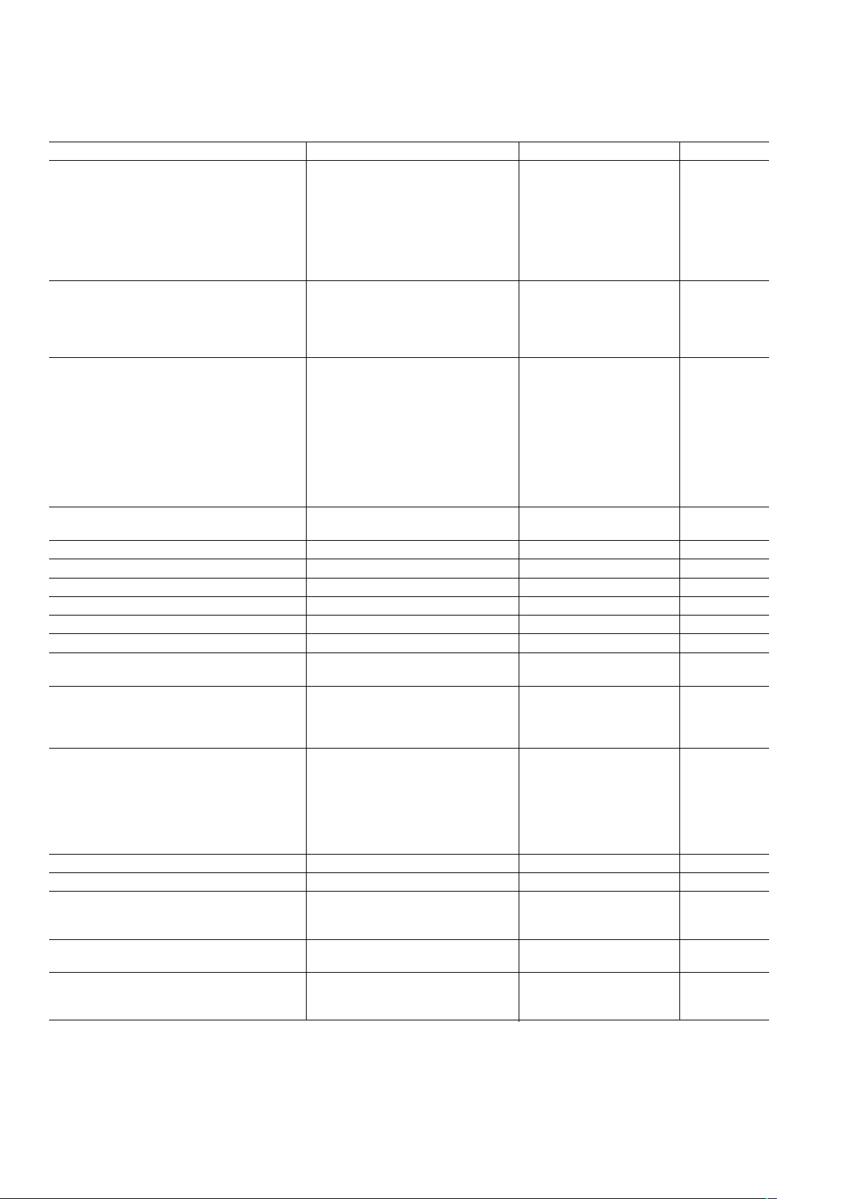
AD807–SPECIFICATIONS
Parameter Condition Min Typ Max Unit
QUANTIZER–DC CHARACTERISTICS
Input Voltage Range @ P
IN
or N
IN
2.5 V
CC
V
Input Sensitivity, V
SENSE
PIN–NIN, Figure 1, BER = ≤ 1 × 10
–10
2mV
Input Overdrive, V
OD
Figure 1, BER = ≤ 1 × 10
–10
0.001 2.5 V
Input Offset Voltage 50 500 µV
Input Current 510µA
Input RMS Noise BER = ≤ 1 × 10
–10
50 µV
Input Peak-to-Peak Noise BER = ≤ 1 × 10
–10
650 µV
QUANTIZER–AC CHARACTERISTICS
Upper –3 dB Bandwidth 180 MHz
Input Resistance 1MΩ
Input Capacitance 2pF
Pulsewidth Distortion 100 ps
LEVEL DETECT
Level Detect Range R
THRESH
= INFINITE 0.8 2 4.0 mV
R
THRESH
= 49.9 kΩ 4 5 7.4 mV
R
THRESH
= 3.4 kΩ 14 20 25 mV
Response Time DC-Coupled 0.1 1.5 µs
Hysteresis (Electrical) R
THRESH
= INFINITE 2.3 4.0 10.0 dB
R
THRESH
= 49.9 kΩ 3.0 5.0 9.0 dB
R
THRESH
= 3.4 kΩ 3.0 7.0 10.0 dB
SDOUT Output Logic High Load = +4 mA 3.6 V
SDOUT Output Logic Low Load = –1.2 mA 0.4 V
PHASE-LOCKED LOOP NOMINAL
CENTER FREQUENCY 155.52 MHz
CAPTURE RANGE 155 156 MHz
TRACKING RANGE 155 156 MHz
STATIC PHASE ERROR 27–1 PRN Sequence 4 20 Degrees
SETUP TIME (tSU) Figure 2 3.0 3.2 3.5 ns
HOLD TIME (tH) Figure 2 3.0 3.1 3.3 ns
PHASE DRIFT 240 Bits, No Transitions 40 Degrees
JITTER 2
7
–1 PRN Sequence 2.0 Degrees RMS
223–1 PRN Sequence 2.0 2.7 Degrees RMS
JITTER TOLERANCE f = 10 Hz 3000 Unit Intervals
f = 6.5 kHz 4.5 7.6 Unit Intervals
f = 65 kHz 0.45 1.0 Unit Intervals
f = 1.3 MHz 0.45 0.67 Unit Intervals
JITTER TRANSFER
Peaking (Figure 11) C
D
= 0.15 µF 0.08 dB
CD = 0.33 µF 0.04 dB
Bandwidth 65 92 130 kHz
Acquisition Time
C
D
= 0.1 µF2
23
–1 PRN Sequence, TA = 25°C4 × 1052 × 106Bit Periods
CD = 0.33 µFV
CC
= 5 V, VEE = GND 2 × 10
6
Bit Periods
POWER SUPPLY VOLTAGE V
MIN
to V
MAX
4.5 5.5 Volts
POWER SUPPLY CURRENT VCC = 5.0 V, VEE = GND, TA = 25°C 25 34.5 39.5 mA
PECL OUTPUT VOLTAGE LEVELS
Output Logic High, V
OH
VCC = 5.0 V, VEE = GND, TA = 25°C –1.2 –1.0 –0.7 Volts
Output Logic Low, V
OL
Referenced to V
CC
–2.0 –1.8 –1.7 Volts
SYMMETRY (Duty Cycle) ρ = 1/2, T
A
= 25°C,
Recovered Clock Output, Pin 5 VCC = 5 V, VEE = GND 50.1 54.1 %
OUTPUT RISE / FALL TIMES
Rise Time (t
R
) 20%–80% 1.1 1.5 ns
Fall Time (tF) 80%–20% 1.1 1.5 ns
Specifications subject to change without notice.
(TA = T
MIN
to T
MAX
, VCC = V
MIN
to V
MAX
, CD = 0.1 F, unless otherwise noted.)

REV. B
AD807
–3–
ABSOLUTE MAXIMUM RATINGS*
Supply Voltage . . . . . . . . . . . . . . . . . . . . . . . . . . . . . . . . . 12 V
Input Voltage (Pin 12 or Pin 13) . . . . . . . . . . . . . V
CC
+ 0.6 V
Maximum Junction Temperature . . . . . . . . . . . . . . . . . 165°C
Storage Temperature Range . . . . . . . . . . . . –65°C to +150°C
Lead Temperature Range (Soldering 10 sec) . . . . . . . . . 300°C
ESD Rating (Human Body Model) . . . . . . . . . . . . . . . . . 500 V
*Stresses above those listed under Absolute Maximum Ratings may cause perma-
nent damage to the device. This is a stress rating only; functional operation of the
device at these or any other conditions above those indicated in the operational
section of this specification is not implied. Exposure to absolute maximum rating
conditions for extended periods may affect device reliability.
Thermal Characteristics:
16-Lead Narrow Body SOIC Package: θJA = 110°C/W.
1
0
OUTPUT
NOISE
OFFSET
OVERDRIVE
SENSITIVITY
INPUT (V)
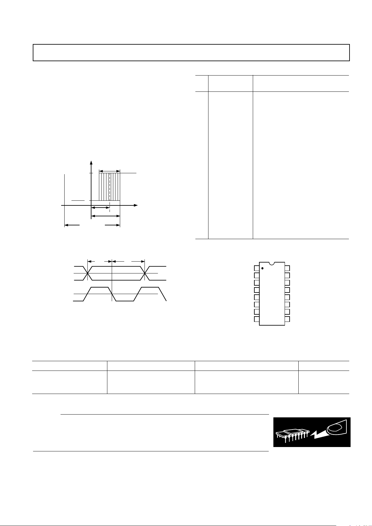
Figure 1. Input Sensitivity, Input Overdrive
SETUP
t
SU
HOLD
t
H
DATAOUTP
(PIN 2)
CLKOUTP
(PIN 5)
Figure 2. Setup and Hold Time
PIN FUNCTION DESCRIPTIONS
Pin
No. Mnemonic Description
1 DATAOUTN Differential Retimed Data Output
2 DATAOUTP Differential Retimed Data Output
3V
CC2
Digital VCC for ECL Outputs
4 CLKOUTN Differential Recovered Clock Output
5 CLKOUTP Differential Recovered Clock Output
6V
CC1
Digital VCC for Internal Logic
7 CF1 Loop Damping Capacitor
8 CF2 Loop Damping Capacitor
9AV
EE
Analog V
EE
10 THRADJ Level Detect Threshold Adjust
11 AV
CC1
Analog VCC for PLL
12 NIN Quantizer Differential Input
13 PIN Quantizer Differential Input
14 AV
CC2
Analog VCC for Quantizer
15 SDOUT Signal Detect Output
16 V
EE
Digital VEE for Internal Logic
PIN CONFIGURATION
TOP VIEW
(Not to Scale)
16
15
14
13
12
11
10
9
1
2
3
4
5
6
7
8
DATAOUTN
DATAOUTP
V
CC2
CLKOUTN
CLKOUTP
V
CC1
CF1
CF2
V
EE
SDOUT
AV
CC2
PIN
NIN
AV
CC1
THRADJ
AV
EE
AD807
ORDERING GUIDE
Model Temperature Range Package Description Package Option
AD807A-155BR –40°C to +85°C 16-Lead Narrowbody SOIC R-16A
AD807A-155BRRL7 –40°C to +85°C 750 Pieces, 7" Reel R-16A
AD807A-155BRRL –40°C to +85°C 2500 Pieces, 13" Reel R-16A
CAUTION
ESD (electrostatic discharge) sensitive device. Electrostatic charges as high as 4000 V readily
accumulate on the human body and test equipment and can discharge without detection. Although
the AD807 features proprietary ESD protection circuitry, permanent damage may occur on devices
subjected to high-energy electrostatic discharges. Therefore, proper ESD precautions are
recommended to avoid performance degradation or loss of functionality.
WARNING!
ESD SENSITIVE DEVICE

REV. B
AD807
–4–
DEFINITION OF TERMS
Maximum, Minimum and Typical Specifications
Specifications for every parameter are derived from statistical
analyses of data taken on multiple devices from multiple wafer
lots. Typical specifications are the mean of the distribution of
the data for that parameter. If a parameter has a maximum (or a
minimum), that value is calculated by adding to (or subtracting
from) the mean six times the standard deviation of the distribution.
This procedure is intended to tolerate production variations: if the
mean shifts by 1.5 standard deviations, the remaining 4.5 standard
deviations still provide a failure rate of only 3.4 parts per million.
For all tested parameters, the test limits are guardbanded to
account for tester variation to thus guarantee that no device is
shipped outside of data sheet specifications.
Input Sensitivity and Input Overdrive
Sensitivity and Overdrive specifications for the Quantizer involve
offset voltage, gain and noise. The relationship between the logic
output of the quantizer and the analog voltage input is shown in
Figure 1.
For sufficiently large positive input voltage the output is always
Logic 1 and similarly, for negative inputs, the output is always
Logic 0. However, the transitions between output Logic Levels 1
and 0 are not at precisely defined input voltage levels, but occur
over a range of input voltages. Within this Zone of Confusion,
the output may be either 1 or 0, or it may even fail to attain
a valid logic state. The width of this zone is determined by the
input voltage noise of the quantizer (650 µV at the 1 × 10
–10
confidence level). The center of the Zone of Confusion is the
quantizer input offset voltage (±500 µV maximum). Input Overdrive is the magnitude of signal required to guarantee correct
logic level with 1 × 10
–10
confidence level.
With a single-ended PIN-TIA (Figure 3), ac coupling is used and
the inputs to the Quantizer are dc biased at some common-mode
potential. Observing the Quantizer input with an oscilloscope
probe at the point indicated shows a binary signal with average
value equal to the common-mode potential and instantaneous
values both above and below the average value. It is convenient
to measure the peak-to-peak amplitude of this signal and call the
minimum required value the Quantizer Sensitivity. Referring to
Figure 1, since both positive and negative offsets need to be
accommodated, the Sensitivity is twice the Overdrive. The AD807
Quantizer has 2 mV Sensitivity.
With a differential TIA (Figure 3), Sensitivity seems to improve
from observing the Quantizer input with an oscilloscope probe.
This is an illusion caused by the use of a single-ended probe. A
1 mV peak-to-peak signal appears to drive the AD807 Quantizer.
However, the single-ended probe measures only half the signal.
The true Quantizer input signal is twice this value since the
other Quantizer input is a complementary signal to the signal being observed.
Response Time
Response time is the delay between removal of the input signal
and indication of Loss of Signal (LOS) at SDOUT. The response
time of the AD807 (1.5 µs maximum) is much faster than the
SONET/SDH requirement (3 µs
≤
response time ≤ 100 µs). In
practice, the time constant of the ac coupling at the Quantizer
input determines the LOS response time.
Nominal Center Frequency
This is the frequency at which the VCO will oscillate with the
loop damping capacitor, C
D
, shorted.
Tracking Range
This is the range of input data rates over which the AD807 will
remain in lock.
Capture Range
This is the range of input data rates over which the AD807 will
acquire lock.
Static Phase Error
This is the steady-state phase difference, in degrees, between the
recovered clock sampling edge and the optimum sampling instant,
which is assumed to be halfway between the rising and falling
edges of a data bit. Gate delays between the signals that define
static phase error, and IC input and output signals prohibit
direct measurement of static phase error.
Data Transition Density, ρ
This is a measure of the number of data transitions, from “0” to
“1” and from “1” to “0,” over many clock periods. ρ is the ratio
(0 ≤ ρ ≤ 1) of data transitions to bit periods.
Jitter
This is the dynamic displacement of digital signal edges from
their long term average positions, measured in degrees rms or
Unit Intervals (UI). Jitter on the input data can cause dynamic
phase errors on the recovered clock sampling edge. Jitter on the
recovered clock causes jitter on the retimed data.
Output Jitter
This is the jitter on the retimed data, in degrees rms, due to a
specific pattern or some pseudorandom input data sequence
(PRN Sequence).
Jitter Tolerance
Jitter Tolerance is a measure of the AD807’s ability to track a
jittery input data signal. Jitter on the input data is best thought
of as phase modulation, and is usually specified in unit intervals.
The PLL must provide a clock signal that tracks the phase
modulation in order to accurately retime jittered data. In order
for the VCO output to have a phase modulation that tracks the
input jitter, some modulation signal must be generated at the
output of the phase detector. The modulation output from the
phase detector can only be produced by a phase error between
its data input and its clock input. Hence, the PLL can never
perfectly track jittered data. However, the magnitude of the
phase error depends on the gain around the loop. At low frequencies, the integrator of the AD807 PLL provides very high
gain, and thus very large jitter can be tracked with small phase
errors between input data and recovered clock. At frequencies
closer to the loop bandwidth, the gain of the integrator is much
smaller, and thus less input jitter can be tolerated. The AD807
output will have a bit error rate less than 1 × 10
–10
when in lock
and retiming input data that has the CCITT G.958 specified
jitter applied to it.
Jitter Transfer (Refer to Figure 11)
The AD807 exhibits a low-pass filter response to jitter applied to
its input data.
 Loading...