ANALOG DEVICES CN-0261 Service Manual

Circuit Note
CN-0261
Ultralow Distortion, Ultralow Noise
Amplifier
ADR435
Ultralow Noise XFET 5 V Reference
Rev.0
Circuits from the Lab™ circuits from Analog Devices have been designed and built by Analog Devices
have been employed in the design and construction of
each circuit, and their function and performance have been tested and verified in a lab environment at
room temperature. However, you are solely responsible for testing the circuit and determining its
uitability and applicability for your use and application. Accordingly, in no event shall Analog Devices
be liable for direct, indirect, special, incidental, consequential or punitive damages due to any cause
whatsoever connected to the use of any Circuits from the Lab circuits. (Continued on last page)
Fax: 781.461.3113 ©2012 Analog Devices, Inc. All rights reserved.
VIN+
VIN–
IN+
IN–
ADR435
5V VREF
VDD = 5V
3-WIRE INTERFACE
SCK
SDO
CNV
VIO
SDI
REF
49.9Ω
VDD
AD8597
GND
9
8
5
10
6
7
2
3
1
4
6
3
2
7
1
3
2
7
1
49.9Ω
49.9Ω
180Ω
180Ω
2.7nF
2.7nF
VCM
0.1µF
590Ω
590Ω
VCM
0.1µF
590Ω
590Ω
1µF
0.1µF
VDD = 8V
VDD = 8V
6
2
4
VIN
GND
VOUT
0.1µF
VDD = 8V
0.1µF
VIO =
1.8V TO 5V
AD7691
AD8597
VSS = –2V
VSS = –2V
22µF
VCM = 2.5V
GND
VREF = 5V
VIN+
VIN–
VCM = VREF ÷ 2
= 2.5V
VCM = VREF ÷ 2
= 2.5V
VOLTAGE DIVIDER
FOR BIASI NG PURPOSES
VOLTAGE DIVIDER
FOR BIASI NG PURPOSES
18-BIT, 1.5LSB INL
250kSPS DIFF ERENTIAL
PulSAR ADC
0.1µF
0.1µF
0.1µF
0.1µF
49.9Ω
10467-001
Circuits from the Lab™ reference circuits are engineered and
tested for quick and easy system integration to help solve today’s
analog, mixed-signal, and RF design challenges. For more
information and/or support, visit www.analog.com/CN0261.
AD7691 18-Bit 1.5 LSB INL, 250 kSPS PulSAR ADC
AD8597
Optimizing AC Performance in an 18-bit, 250 kSPS, PulSAR Measurement Circuit
Devices Connected/Referenced
EVALUATION AND DESIGN SUPPORT
Circuit Evaluation Boards
CN-0261 Circuit Evaluation Board (EVAL-CN0261-SDPZ)
System Demonstration Platform (EVAL-SDP-CB1Z)
Design and Integration Files
Schematics, Layout Files, Bill of Materials
CIRCUIT FUNCTION AND BENEFITS
Choosing complementary products for high performance ADCs
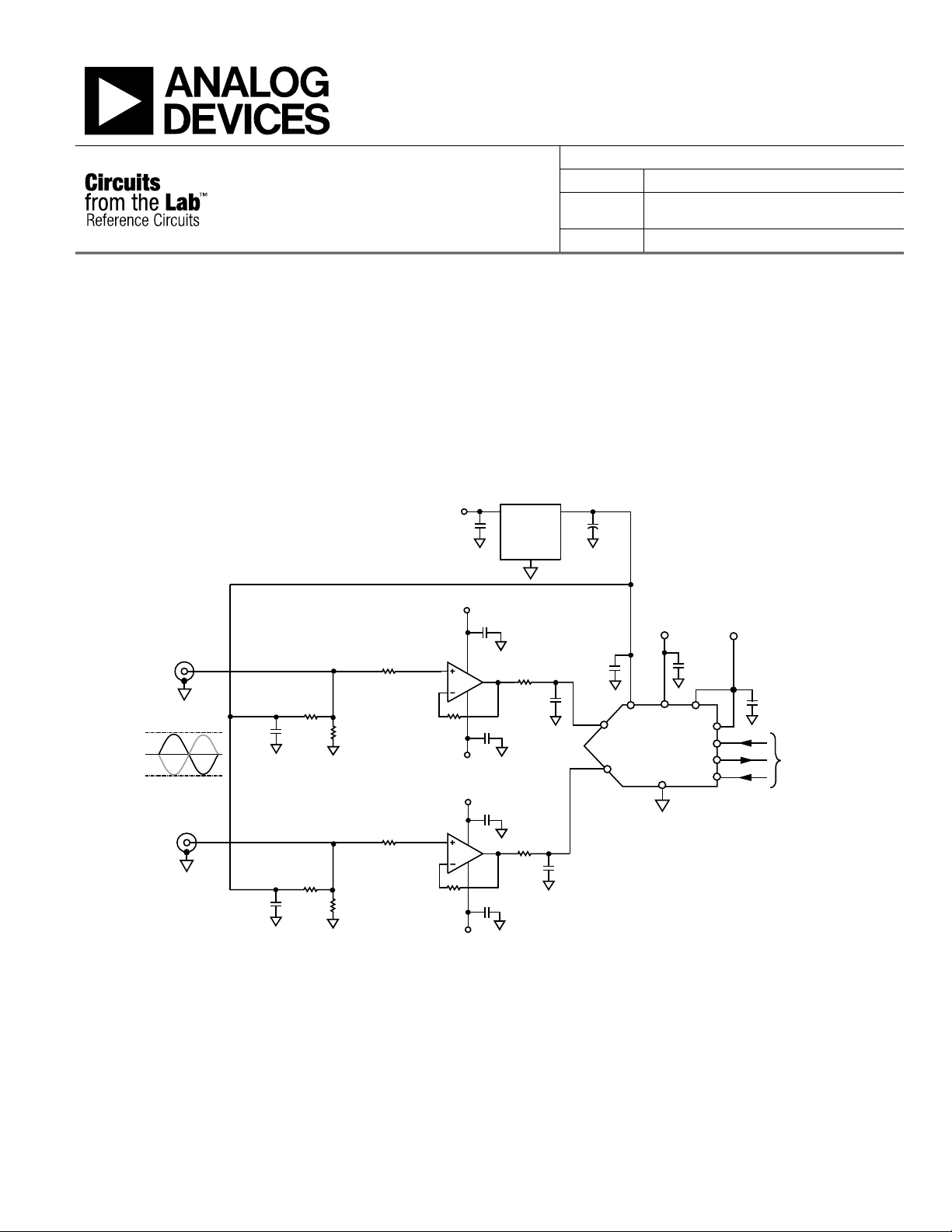
can be a challenge. The circuit in Figure 1 shows a complete
front end solution for the 18-bit, 250 kSPS PulSAR® ADC,
which is optimized for ac performance.
engineers. Standard engineering practices
s
Figure 1. High Performance, 18-Bit ADC Front End (Simplified Schematic: All Connections and Decoupling Not Shown)
One Technology Way, P.O. Box 9106, Norwood, MA 02062-9106, U.S.A.
Tel: 781.329.4700
www.analog.com

CN-0261 Circuit Note
10467-002
–250
–200
–150
–100
0
–50
0 20 40 60
FREQUENCY (kHz)
AMPLITUDE (dB)
80 100 120
10467-003
FUNDAMENTAL = 1kHz, –0.3dB
FROM FS
SAMPLING FREQUENCY = 250kSPS
SNR = 101.02dB
THD = –118.44dB
SINAD = 100.94dB
DYNAMIC RANGE = 101.5dB
The circuit centers on the AD7691, which is a low power ADC
(1.35 mW @ 2.5 V and 100 kSPS) from the PulSAR family.
The ADC is driven directly from the AD8597 ultralow
distortion, ultralow noise amplifier, and the ADC’s reference is
the ultralow noise 5 V ADR435. The circuit achieves 101 dB
SNR and 118 dB THD with a 1 kHz input tone.
CIRCUIT DESCRIPTION
The heart of this circuit is the AD7691, an 18-bit, 250 kSPS
charge redistribution, successive approximation, analog-todigital converter (ADC) that operates from a single power
supply.
It contains a low power, high speed, 18-bit sampling ADC with
no missing codes, an internal conversion clock, and a versatile
serial interface port. On the CNV rising edge, it samples the
voltage difference between the IN+ and IN− pins. The voltages
on these pins swing in opposite phases between 0 V and REF.
The reference voltage, REF, is applied externally and can be set
up to the supply voltage. The AD7691 power scales linearly with
throughput.
For the experiments carried out for this circuit note, the
AD7691was interfaced to the SDP (System Demonstration
Platform board, EVA L-SDP-CB1Z), and the ADC SPIcompatible serial interface was connected to the DSP SPORT
interface VIO supply.
The AD7691 is housed in a 10-lead MSOP or a 10-lead QFN
(LFCSP).
The ADC is driven from the AD8597 (4.8 mA/amplifier), which
is a low noise, low distortion operational amplifiers ideal for use
as an input buffer. The low noise of 1.1 nV/√Hz and low
harmonic distortion of less than −120 dB at audio frequencies
give the AD8597 the wide dynamic range necessary for
preamplifiers in audio, medical, and instrumentation
applications. The excellent slew rate of 14 V/μs and 10 MHz
gain bandwidth product make it highly suitable for medical
applications.
The AD8597 can be operated on supply voltages up to ±15 V. In
the circuit, supply voltages of +8 V and −2 V were chosen in
order to minimize power dissipation.
The AD8597 is available in 8-lead SOIC and LFCSP packages.
The 180 Ω resistors and the 2.7 nF capacitors form a single-pole
327 kHz low-pass filter to further reduce noise.
The voltage reference used in this application is the ADR435,
which is one of a family of XFET® voltage references featuring
low noise, high accuracy, and low temperature drift
performance. Using patented temperature drift curvature
correction and XFET (eXtra implanted junction FET)
technology, voltage change vs. temperature is minimized.
The ADR43x family can source up to 30 mA of output current
and sink up to 20 mA. It also has a trim terminal to adjust the
output voltage over a 0.5% range without compromising
performance.
The ADR435 is available in either an 8-lead MSOP or an 8-lead
narrow SOIC package.
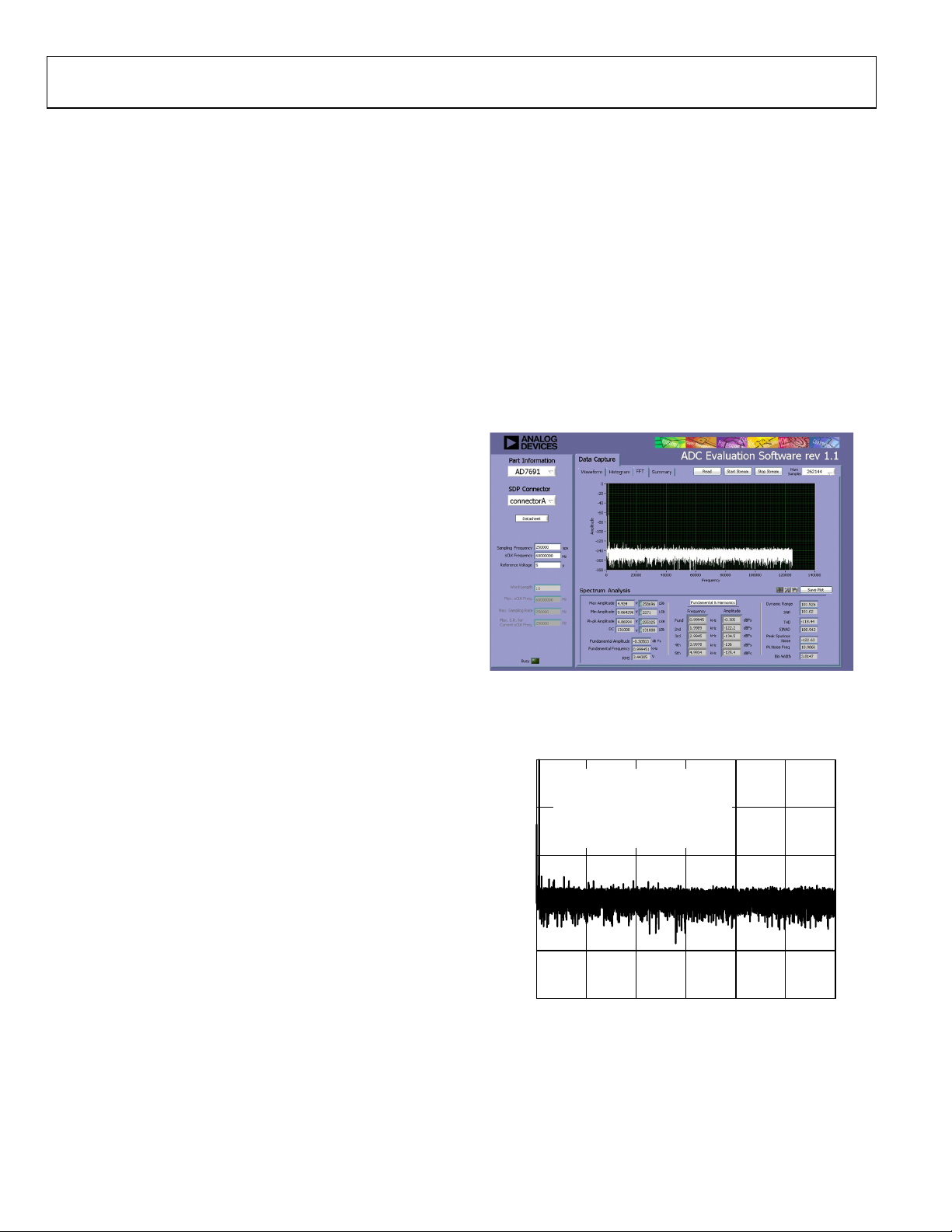
The dynamic performance of the above configuration is shown
in Figure 2 and Figure 3 and is summarized below:
SNR = 101.02dB
THD = 118.44 dB
SINAD = 100.94 dB
Dynamic Range = 101.5 dB
Figure 2. Evaluation Board Software Output Screen Capture
Figure 3. FFT Details for 1 kHz Tone Sampling at 250 kSPS
Rev. 0 | Page 2 of 4
 Loading...