

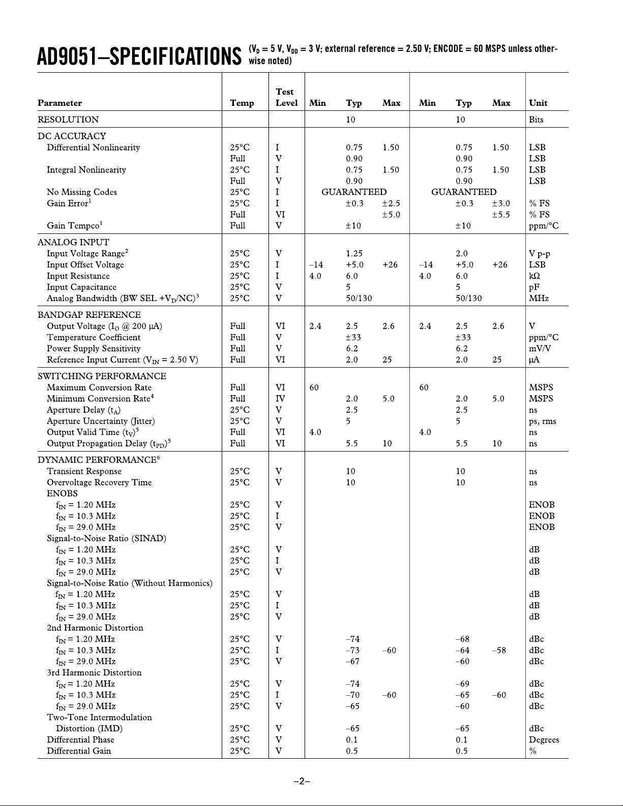
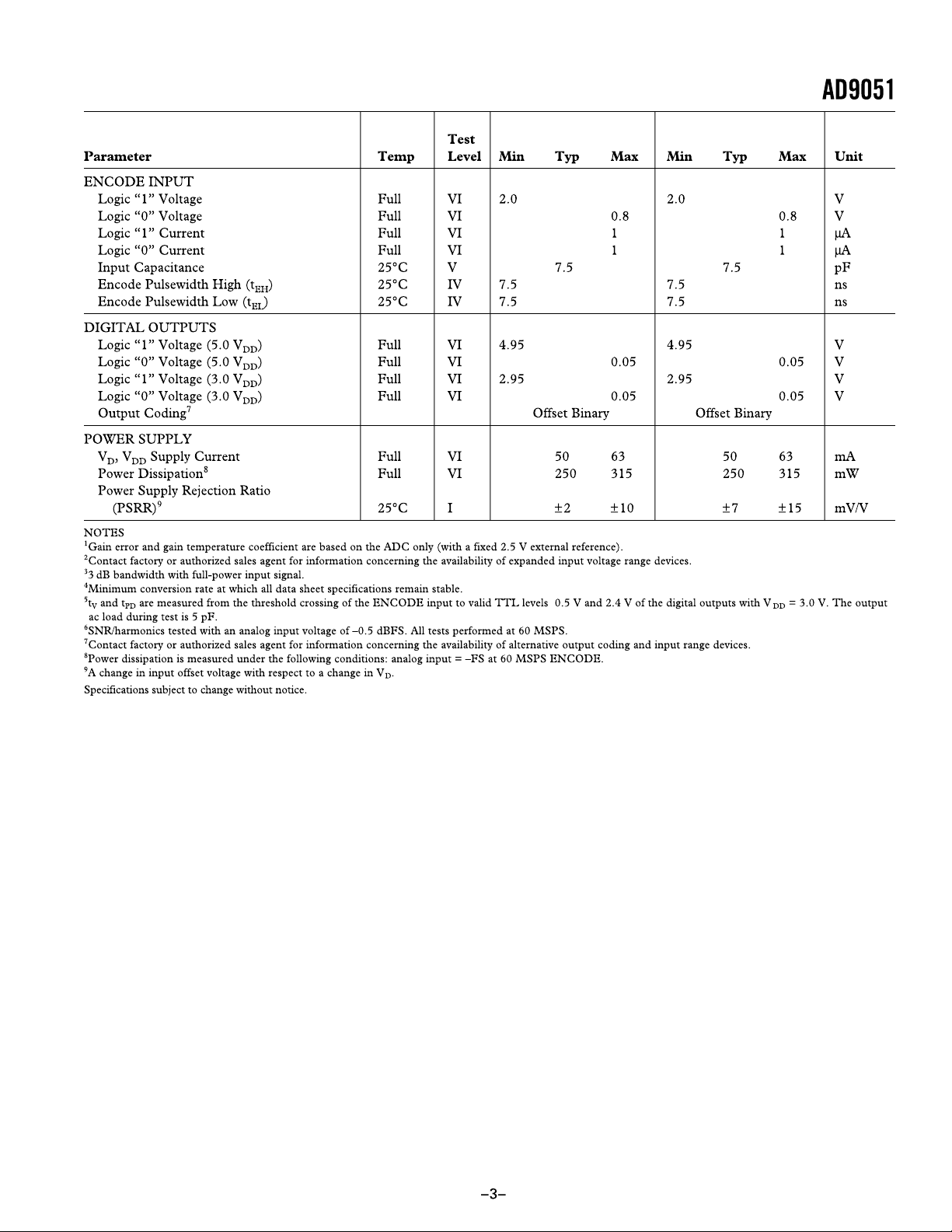
10-Bit, 60 MSPS
2010
781/461-3113
C
a
FEATURES
60 MSPS Sampling Rate
9.3 Effective Number of Bits at f
250 mW Total Power at 60 MSPS
Selectable Input Bandwidth of 50 MHz or 130 MHz
On-Chip T/H and Voltage Reference
Single 5 V Supply Voltage
5 V or 3 V Logic I/O Compatible
Input Range and Output Coding Options Available
APPLICATIONS
Medical Imaging
Digital Communications
Professional Video
Instrumentation
Set-Top Box
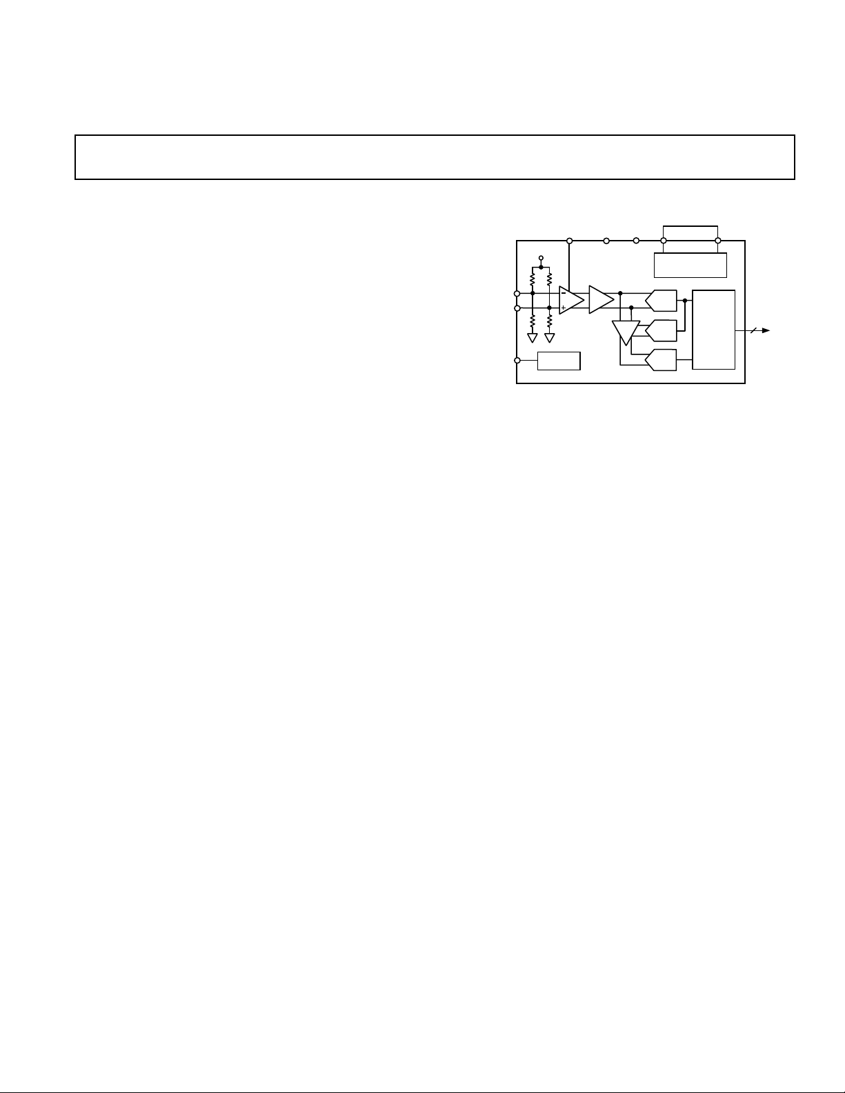
GENERAL DESCRIPTION
The AD9051 is a complete 10-bit monolithic sampling analogto-digital converter (ADC) with an onboard track-and-hold and
reference. The unit is designed for low cost, high performance
applications and requires only 5 V and an encode clock to
achieve 60 MSPS sample rates with 10-bit resolution.
The encode clock is TTL compatible and the digital outputs are
CMOS; both can operate with 5 V/3 V logic. The two-step
architecture used in the AD9051 is optimized to provide the
best dynamic performance available while maintaining low
power consumption.
= 10.3 MHz
IN
A/D Converter
AD9051
FUNCTIONAL BLOCK DIAGRAM
BWSEL
5V
AINB
AIN
ENCODE
TIMING
A 2.5 V reference is included onboard, or the user can provide
an external reference voltage for gain control or matching of
multiple devices. Fabricated on a state-of-the-art BiCMOS
process, the AD9051 is packaged in a space saving surface
mount package (SSOP) and is specified over the industrial temperature range (–40°C to +85°C).
5V GND
AD9051
T/H
SUM
AMP
IN OUT
REFERENCE
CIRCUITS
ADC
DAC
ADC
DECODE
LOGIC
10
REV.
Information furnished by Analog Devices is believed to be accurate and
reliable. However, no responsibility is assumed by Analog Devices for its
use, nor for any infringements of patents or other rights of third parties that
may result from its use. No license is granted by implication or otherwise
under any patent or patent rights of Analog Devices.
One Technology Way, P.O. Box 9106, Norwood, MA 02062-9106, U.S.A.
Tel: 781/329-4700 www.analog.com
Fax: © Analog Devices, Inc.,
AD9051BRS/
AD9051BRSZ
AD9051BRS-2V/
AD9051BRSZ-2V
8.76
53.5
54.5
9.3
9.0
8.8
56.5
56
54
55.5
56.5
55
8.59
52.5
53.5
9.1
8.8
8.6
56.5
55
53
56.5
55.5
54
REV. C
AD9051BRS/
AD9051BRSZ
AD9051BRS-2V/
AD9051BRSZ-2V
REV. C

AD9051
WARNING!
ESD SENSITIVE DEVICE
C
ABSOLUTE MAXIMUM RATINGS*
VD, VDD . . . . . . . . . . . . . . . . . . . . . . . . . . . . . . . . . . . . . . 7 V
Analog Inputs . . . . . . . . . . . . . . . . . . . . –0.5 V to V
Digital Inputs . . . . . . . . . . . . . . . . . . . . . . . . . . . –0.5 V to V
VREF Input . . . . . . . . . . . . . . . . . . . . . . . . . . . . . –0.5 V to V
Digital Output Current . . . . . . . . . . . . . . . . . . . . . . . . 20 mA
Operating Temperature . . . . . . . . . . . . . . . . –55°C to +125°C
Storage Temperature . . . . . . . . . . . . . . . . . . –65°C to +150°C
Maximum Junction Temperature . . . . . . . . . . . . . . . . . 150°C
Maximum Case Temperature . . . . . . . . . . . . . . . . . . . . 150°C
*Stresses above those listed under Absolute Maximum Ratings may cause perma-
nent damage to the device. This is a stress rating only; functional operation of the
device at these or any other conditions above those indicated in the operational
sections of this specification is not implied. Exposure to absolute maximum ratings
for extended periods may effect device reliability.
Table I. Digital Coding (Single-Ended Input with AIN, AINB Bypassed to GND)
+ 0.5 V
D
D
D
EXPLANATION OF TEST LEVELS
Test Level
I. 100% production tested.
II. 100% production tested at 25°C and sample tested at
specified temperatures.
III. Sample tested only.
IV. Parameter is guaranteed by design and characterization
testing.
V. Parameter is a typical value only.
VI. 100% production tested at 25°C; guaranteed by design and
characterization testing for industrial temperature range.
OR Digital Output
Analog Input Voltage Level (Out of Range) MSB... LSB
3.126 (3.50)* Positive Full Scale + 1 LSB 1 1111111111
2.5 Midscale 0 0111111111
1.874 (1.50)* Negative Full Scale – 1 LSB 1 0000000000
*(BRS-2V Version)
CAUTION
ESD (electrostatic discharge) sensitive device. Electrostatic charges as high as 4000 V readily
accumulate on the human body and test equipment and can discharge without detection. Although
the AD9051 features proprietary ESD protection circuitry, permanent damage may occur on
devices subjected to high-energy electrostatic discharges. Therefore, proper ESD precautions are
recommended to avoid performance degradation or loss of functionality.
–4–
REV.

AD9051
C
PIN FUNCTION DESCRIPTIONS
Pin No. Mnemonic Description
1, 6, 7, 12, 21, 23 GND Ground
2, 8, 11 V
D
3 VREFOUT Internal Bandgap Voltage Reference (Nominally 2.5 V)
4 VREFIN Input to Reference Amplifier. Voltage reference for ADC is connected here.
5 BWSEL Bandwidth Select. NC = 130 MHz nominal. +V
9 AINB Complementary Analog Input Pin (Analog Input Bar)
10 AIN Analog Input Pin
13 ENCODE Encode Clock Input to ADC. Internal T/H is placed in hold mode (ADC is encoding)
14 OR Out of Range Signal. Logic “0” when analog input is in nominal range. Logic “1” when
15 D9 (MSB) Most Significant Bit of ADC Output
16–19 D8–D5 Digital Output Bits of ADC
20, 22 V
DD
24–27 D4–D1 Digital Output Bits of ADC
28 D0 (LSB) Least Significant Bit of ADC Output
Analog 5 V Power Supply
= 50 MHz nominal.
D
on rising edge of encode signal.
analog input is out of nominal range.
Digital Output Power Supply (Only Used by Digital Outputs)
PIN CONFIGURATION
GND
VREFOUT
VREFIN
BWSEL
GND
GND
AINB
AIN
GND
ENCODE
OR
V
D
V
D
V
D
1
2
3
4
5
6
AD9051
7
TOP VIEW
8
(Not to Scale)
9
10
11
12
13
14
28
27
26
25
24
23
22
21
20
19
18
17
16
15
D0 (LSB)
D1
D2
D3
D4
GND
V
DD
GND
V
DD
D5
D6
D7
D8
D9 (MSB)
AIN
ENCODE
DIGITAL
OUTPUTS
AINB (PIN 9)
AIN (PIN 10)
N N + 1 N + 2 N + 3 N + 4 N + 5
t
A
tEHt
EL
t
PD
N – 5 N – 4 N – 3 N – 2 N – 1 N
Figure 1. Timing Diagram
V
D
12k⍀
12k⍀
INPUT
12k⍀
BUFFER
12k⍀
ENCODE
(PIN 13)
Analog Input Encode
VDD (PINS 20, 22)
+3V TO +5V
V
D
V
D
D0–D9, OR
VREF
(PIN 3)
OUT
Output Stage VREF
Figure 2. Equivalent Circuits
REV.
–5–

AD9051
C
255
250
245
240
235
230
225
DISSIPATION – mW
220
215
210
15
15
20 25 30 35 40 45 50 55 60
CLOCK RATE – MSPS
ADC GAIN – dB
0
–1
BWSEL DISABLED
–2
–3
BWSEL ENABLED
–4
–5
–6
1
40 52 80 118 141
ANALOG INPUT FREQUENCY – MHz
201
TPC 1. Power Dissipation vs. Clock Rate
60
SNR/SINAD – dB
59
58
57
56
55
54
53
52
51
50
0
SINAD @ 60MSPS
SNR @ 60MSPS
20 30 40 50 60 70 80
FREQUENCY – MHz
SNR @ 40MSPS
SINAD @ 40MSPS
TPC 2. SNR/SINAD vs. AIN Frequency
–50
–55
–60
–65
–70
–75
dB
–80
–85
–90
–95
–100
3RD @ 40MSPS
0
2ND @ 60MSPS
2ND @ 40MSPS
3RD @ 60MSPS
20 30 40 50 60 70 80
FREQUENCY – MHz
TPC 3. Harmonics vs. AIN Frequency
TPC 4. ADC Gain vs. AIN Frequency
59
58.5
58
57.5
57
SNR – dB
56.5
56
55.5
9010
55
–40
ENCODE = 60MSPS
ENCODE = 40MSPS
TEMPERATURE – ⴗC
AIN = 10.3MHz
45250–20
65
85
TPC 5. SNR vs. Temperature
60
59
58
57
56
55
SNR – dB
54
53
52
51
9010
50
5
40302010
ENCODE – MSPS
AIN = 10.3MHz
50 60
70
TPC 6. SNR vs. Clock Rate
–6–
REV.

AD9051
FREQUENCY – MHz
0
–10
–40
–100
–30
–90
–20
–50
–80
–70
–60
dB
AIN = 21.7MHz
ENCODE = 60MSPS
SNR = 57.76dB
SINAD = 56.27dB
0 3.8 7.5 11.3 15.0 18.8 22.5 26.3 30
FREQUENCY – MHz
0
–10
–40
–100
–30
–90
–20
–50
–80
–70
–60
dB
AIN1 = 9.5MHz, –7dBFS
AIN2 = 9.9MHz, –7dBFS
IMD = –65dBc
ENCODE = 60MSPS
0 3.8 7.5 11.3 15.0 18.8 22.5 26.3 30
C
0
–10
AIN = 10.3MHz
ENCODE = 40MSPS
SNR = 58.6dB
–20
SINAD = 57.69dB
–30
–40
–50
dB
–60
–70
–80
–90
–100
0 2.5 5.0 7.5 10 12.5 15 17.5 20
FREQUENCY – MHz
TPC 7. FFT Plot 40 MSPS, 10.3 MHz
0
–10
AIN = 15.2MHz
ENCODE = 40MSPS
SNR = 58.47dB
–20
SINAD = 57.04dB
–30
–40
–50
dB
–60
–70
–80
–90
–100
0 2.5 5.0 7.5 10 12.5 15 17.5 20
FREQUENCY – MHz
0
AIN = 15.2MHz
–10
ENCODE = 60MSPS
SNR = 58.29dB
–20
SINAD = 57.23dB
–30
–40
–50
dB
–60
–70
–80
–90
–100
0 3.8 7.5 11.3 15.0 18.8 22.5 26.3 30
FREQUENCY – MHz
TPC 10. FFT Plot 60 MSPS, 15.2 MHz
TPC 8. FFT Plot 40 MSPS, 15.2 MHz
0
–10
–20
–30
–40
–50
dB
–60
–70
–80
REV.
–90
–100
0 3.8 7.5 11.3 15.0 18.8 22.5 26.3 30
TPC 9. FFT Plot 60 MSPS, 10.3 MHz
AIN = 10.3MHz
ENCODE = 60MSPS
SNR = 58.15dB
SINAD = 57.25dB
FREQUENCY – MHz
TPC 11. FFT Plot 60 MSPS, 21.7 MHz
TPC 12. Two-Tone IMD
–7–

AD9051
C
1.2
6.5
1.0
0.8
0.6
% GAIN ERROR
0.4
0.2
0
0
16
14
12
10
8
6
OFFSET – mV
4
2
0
0
20 30 40 50
ENCODE – MSPS
TPC 13. Gain vs. Clock Rate
20 30 40 50
ENCODE – MSPS
5V RISING
3V RISING
45250–20
85
65
6
5.5
5V FALLING
– ns
PD
t
5
3V FALLING
4.5
6010
4
–40
TEMPERATURE – ⴗC
TPC 16. tPD vs. Temperature 3 V/5 V
2.51
2.50
2.49
2.48
2.47
2.46
REF VOLTAGE
2.45
2.44
2.43
2.42
6010
0.1
0.55 0.7 0.85 1 1.15 1.3 1.45 1.6 1.75 1.9 2.0
0.25 0.4
SOURCE CURRENT – mA
V
OUT
SNR – dB
60
58
56
54
52
50
48
46
44
42
40
TPC 14. Offset vs. Clock Rate
SNR @ 40MSPS
25 5530
35 40 45 50
DUTY CYCLE – %
TPC 15. SNR vs. Duty Cycle
SNR @ 60MSPS
60 65 70 75
TPC 17. Reference Load Regulation
80
70
60
50
40
30
% OCCURRANCE
20
10
0
512 513 514 515 516 517 518
CODE
TPC 18. Midscale Histogram (Inputs Tied)
–8–
REV.

AD9051
C
THEORY OF OPERATION
Refer to the block diagram on the front page.
The AD9051 employs a subranging architecture with digital
error correction. This combination of design techniques ensures
true 10-bit accuracy at the digital outputs of the converter.
At the input, the analog signal is buffered by a high speed
differential buffer and applied to a track-and-hold (T/H) that
holds the analog value present when the unit is strobed with
an ENCODE command. The conversion process begins on the
rising edge of this pulse. The two stage architecture completes a
coarse and then a fine conversion of the T/H output signal.
Error correction and decode logic correct and align data from
the two conversions and present the result as a 10-bit parallel
digital word. Output data are strobed on the rising edge of the
ENCODE command. The subranging architecture results in
five pipeline delays for the output data. Refer to the AD9051
Timing Diagram.
USING THE AD9051
3 V System
The digital input and outputs of the AD9051 can be easily
configured to directly interface to 3 V logic systems. The encode
input (Pin 13) is TTL compatible with a logic threshold of
1.5 V. This input is actually a CMOS stage (refer to Equivalent
Encode Input Stage) with a TTL threshold, allowing operation
with TTL, CMOS and 3 V CMOS logic families. Using 3 V
CMOS logic allows the user to drive the encode directly without
the need to translate to 5 V. This saves the user power and
board space. As with all high speed data converters, the clock
signal must be clean and jitter free to prevent the degradation of
dynamic performance.
The AD9051 outputs can also directly interface to 3 V logic
systems. The digital outputs are standard CMOS stages (refer
to AD9051 Output Stage) with isolated supply pins (Pins 20,
22 V
). By varying the voltage on the VDD pins, the digital
DD
output levels vary respectively. By connecting Pins 20 and 22 to
the 3 V logic supply, the AD9051 will supply 3 V output
levels. Care should be taken to filter and isolate the output
supply of the AD9051 as noise could be coupled into the
ADC, limiting performance.
Analog Input
The analog input of the AD9051 is a differential input buffer
(refer to AD9051 Equivalent Analog Input). The differential
inputs are internally biased at 2.5 V, obviating the need for
external biasing. Excellent performance is achieved whether the
analog inputs are driven single-endedly or differentially (for
best dynamic performance, impedances at AIN and AINB
should match).
Figure 3 shows typical connections for the analog inputs when
using the AD9051 in a dc-coupled system with single-ended
signals. All components are powered from a single 5 V supply.
The AD820 is used to offset the ground referenced input signal
to the level required by the AD9051.
AC coupling of the analog inputs of the AD9051 is easily
accomplished. Figure 4 shows capacitive coupling of a singleended signal while Figure 5 shows transformer coupling
differentially into the AD9051.
140⍀
V
IN
–0.625V
TO
+0.625V
140⍀
0.1F
1k⍀
1k⍀
5V
AD9631
5V
AD820
5V
10
AD9051
9
0.1F
Figure 3. Single Supply, Single-Ended, DC-Coupled
AD9051
140⍀
V
IN
–0.625V
TO
+0.625V
140⍀
+5V
–5V
0.1F
AD9631
0.1F
5V
10
AD9051
9
Figure 4. Single-Ended, Capacitively-Coupled AD9051
140⍀
V
IN
–0.625V
TO
+0.625V
140⍀
+5V
–5V
AD9631
0.1F
T1-1T
50⍀
5V
10
AD9051
9
Figure 5. Differentially Driven AD9051 Using Transformer Coupling
The AD830 provides a unique method of providing dc level
shift for the analog input. Using the AD830 allows a great deal
of flexibility for adjusting offset and gain. Figure 6 shows the
AD830 configured to drive the AD9051. The offset is provided
by the internal biasing of the AD9051 differential input (Pin 9).
For more information regarding the AD830, see the AD830
data sheet.
V
IN
–0.625V
TO
+0.625V
1
2
3
4
+15V
AD830
–5V
7
10
9
0.1F
+5V
AD9051
Figure 6. Level-Shifting with the AD830
REV.
–9–

AD9051
C
Overdrive of the Analog Input
Special care was taken in the design of the analog input section
of the AD9051 to prevent damage and corruption of data when
the input is overdriven. The nominal input range is 1.875 V to
3.125 V (1.25 V p-p centered at 2.5 V). Out-of-range comparators detect when the analog input signal is out of this range and
the input buffer is clamped. The digital outputs are locked at
their maximum or minimum value (i.e., all “0” or all “1”). This
precludes the digital outputs changing to an invalid value when
the analog input is out of range.
The input is protected to one volt outside the power supply
rails. For nominal power (5 V and ground), the analog input
will not be damaged with signals from +5.5 V to –0.5 V.
Timing
The performance of the AD9051 is very insensitive to the duty
cycle of the clock. Pulsewidth variations of as much as ±15% for
encode rates of 40 MSPS and ±10% for encode rates of 60 MSPS
will cause no degradation in performance. (See Figure 17, SNR vs.
Duty Cycle.)
The AD9051 provides latched data outputs, with five pipeline
delays. Data outputs are available one propagation delay (t
after the rising edge of the encode command (refer to Figure 1,
Timing Diagram). The length of the output data lines and
loads placed on them should be minimized to reduce transients within the AD9051; these transients can detract from
the converter’s dynamic performance.
Power Dissipation
The power dissipation specification in the parameter table is
measured under the following conditions: encode is 60 MSPS,
analog input is –FS.
As shown in Figure 3, the actual power dissipation varies based
on these conditions. For instance, reducing the clock rate will
reduce power as expected for CMOS-type devices. The loading
determines the power dissipated in the output stages.
The analog input frequency and amplitude in conjunction with
the clock rate determine the switching rate of the output data
bits. Power dissipation increases as more data bits switch at
faster rates. For instance, if the input is a dc signal that is out of
range, no output bits will switch. This minimizes power in the
output stages, but is not realistic from a usage standpoint.
The dissipation in the output stages can be minimized by interfacing the outputs to 3 V logic (refer to Using the AD9051, 3 V
System). The lower output swings minimize power consumption
as follows: (1/2 C
Voltage Reference
LOAD
2
× V
× Update Rate).
DD
A stable and accurate 2.5 V voltage reference is built into the
AD9051 (Pin 3, VREFOUT). In normal operation the internal
reference is used by strapping together Pins 3 and 4 of the
AD9051. The internal reference has 500 µA of extra drive cur-
rent that can be used for other circuits.
PD
)
Some applications may require greater accuracy, improved
temperature performance, or adjustment of the gain of the
AD9051, which cannot be obtained by using the internal reference. For these applications, an external 2.5 V reference can be
used to connect to Pin 4 of the AD9051. The VREFIN requires
2 µA of drive current.
The input range can be adjusted by varying the reference
voltage applied to the AD9051. No appreciable degradation
in performance occurs when the reference is adjusted ±5%.
The full-scale range of the ADC tracks reference voltage
changes linearly.
–10–
REV.

AD9051
OUTLINE DIMENSIONS
10.50
10.20
9.90
0.38
0.22
15
5.60
5.30
8.20
5.00
7.80
1.85
1.75
1.65
SEATING
PLANE
7.40
0.25
0.09
8°
4°
0°
0.95
0.75
0.55
060106-A
14
2.00 MAX
0.05 MIN
COPLANARITY
0.10
28
1
0.65 BSC
COMPLIANT TO JEDEC STANDARDS MO-150-AH
Figure 7.28-Lead Shrink Small Outline Package [SSOP]
(RS-28)
Dimensions shown in millimeters
ORDERING GUIDE
Model1 Temperature Range Package Description Package Option
AD9051BRS −40°C to +85°C 28-Lead Shrink Small Outline Package (SSOP) RS-28
AD9051BRS-2V −40°C to +85°C 28-Lead Shrink Small Outline Package (SSOP) RS-28
AD9051BRSRL −40°C to +85°C 28-Lead Shrink Small Outline Package (SSOP) RS-28
AD9051BRSZ −40°C to +85°C 28-Lead Shrink Small Outline Package (SSOP) RS-28
AD9051BRSZRL −40°C to +85°C 28-Lead Shrink Small Outline Package (SSOP) RS-28
AD9051BRSRL-2V −40°C to +85°C 28-Lead Shrink Small Outline Package (SSOP) RS-28
AD9051BRSZ-2V −40°C to +85°C 28-Lead Shrink Small Outline Package (SSOP) RS-28
AD9051BRSZRL-2V −40°C to +85°C 28-Lead Shrink Small Outline Package (SSOP) RS-28
1
Z = RoHS Compliant Part.
REVISION HISTORY
11/10—Rev. B to Rev. C
Changes to Specifications Section ................................................... 2
Deleted Evaluation Board Section ................................................ 10
Updated Outline Dimensions ........................................................ 11
Changes to Ordering Guide ........................................................... 11
7/01—Rev. A to Rev. B
Edits to ABSOLUTE MAXIMUM RATINGS ............................... 4
©2010 Analog Devices, Inc. All rights reserved. Trademarks and
registered trademarks are the property of their respective owners.
D00558-0-11/10(C)
REV. C –11–
 Loading...