Analog Devices AD9049 Datasheet

a
9-Bit, 30 MSPS ADC
AD9049
FEATURES
Low Power: 300 mW
On-Chip T/H, Reference
Single +5 V Power Supply Operation
Selectable 5 V or 3 V Logic I/O
Wide Dynamic Performance
APPLICATIONS
Digital Communications
Professional Video
Medical Imaging
Instrumentation
PRODUCT DESCRIPTION
The AD9049 is a complete 9-bit monolithic sampling analogto-digital converter (ADC) with an onboard track-and-hold and
reference. The unit is designed for low cost, high performance
applications and requires only +5 V and an encode clock to
achieve 30 MSPS sample rates with 9-bit resolution.
The encode clock is TTL compatible and the digital outputs
are CMOS; both can operate with 5 V/3 V logic, selected by the
user. The two-step architecture used in the AD9049 is optimized to provide the best dynamic performance available while
maintaining low power consumption.
A 2.5 V reference is included onboard, or the user can provide
an external reference voltage for gain control or matching of
multiple devices. Fabricated on an advanced BiCMOS process,
the AD9049 is packaged in space saving surface mount packages (SOIC, SSOP) and is specified over the industrial
(–40°C to +85°C) temperature range.
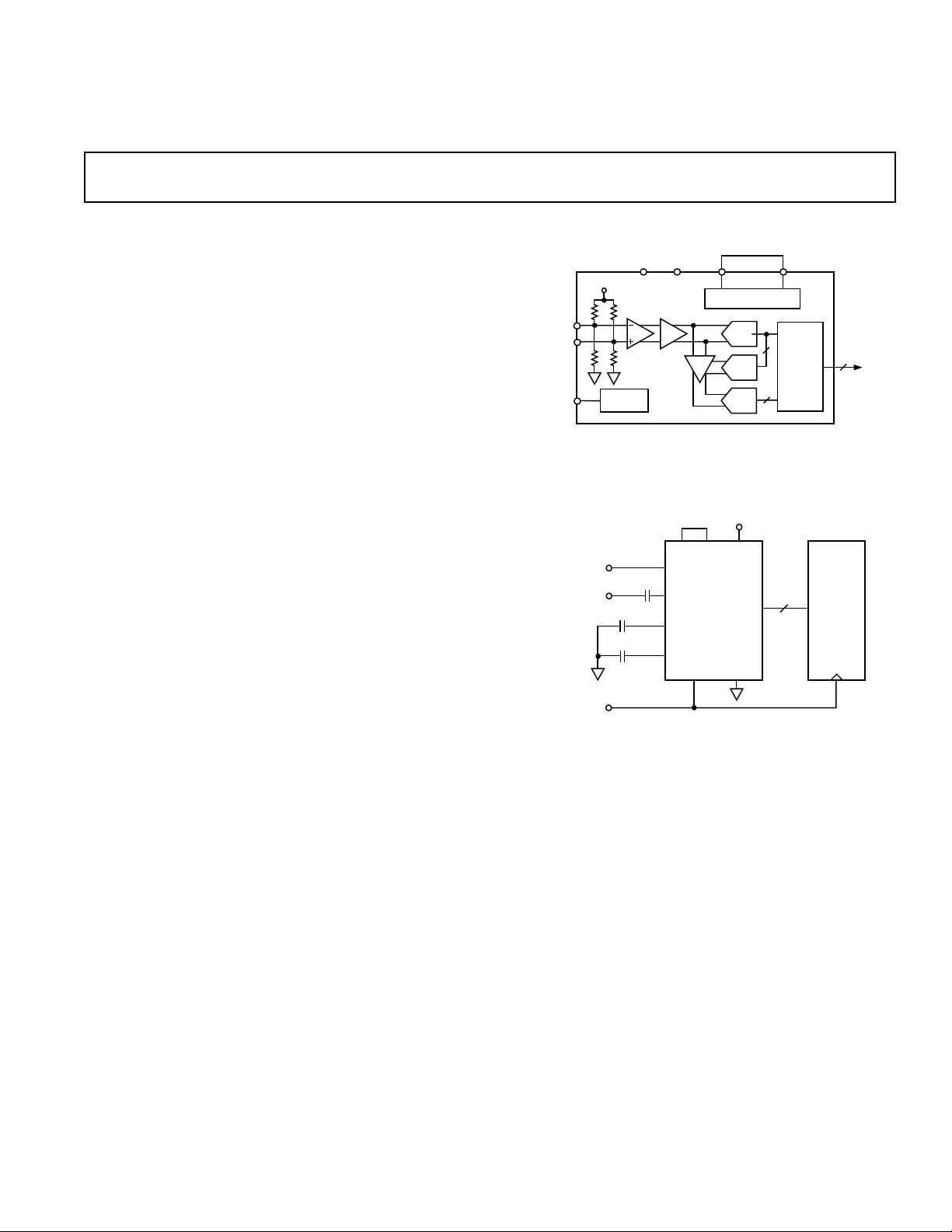
FUNCTIONAL BLOCK DIAGRAM
AINB
AIN
ENCODE
(+3.3V ± 0.512V)
ENCODE
GND
+5V
+5V
AD9049
T/H
TIMING
AIN
0.1µF
+5V
0.1µF
0.1µF
SUM
AMP
10
5
6
9
3
13
REFERENCE CKTS
ADC
DAC
ADC
+5V
2, 8, 11,
4
20, 22
AD9049
1, 7, 12,
21, 23
Figure 1. Typical Connections
DECODE
9 BITS
LOGIC
9
(2)
74AC574
REV. A
Information furnished by Analog Devices is believed to be accurate and
reliable. However, no responsibility is assumed by Analog Devices for its
use, nor for any infringements of patents or other rights of third parties
which may result from its use. No license is granted by implication or
otherwise under any patent or patent rights of Analog Devices.
One Technology Way, P.O. Box 9106, Norwood, MA 02062-9106, U.S.A.
Tel: 617/329-4700 World Wide Web Site: http://www.analog.com
Fax: 617/326-8703 © Analog Devices, Inc., 1996

AD9049–SPECIFICATIONS
ELECTRICAL CHARACTERISTICS
(VD, VDD = +5 V; internal reference; ENCODE = 30 MSPS unless otherwise noted)
Test AD9049BR/BRS
Parameter Temp Level Min Typ Max Units
RESOLUTION 9 Bits
DC ACCURACY
Differential Nonlinearity +25°C I 0.5 1.0 LSB
Full V 0.5 LSB
Integral Nonlinearity +25°C I 0.5 1.0 LSB
Full V 0.5 LSB
No Missing Codes Full IV GUARANTEED
Gain Error +25°CI ±1.0 ±7.5 % FS
Gain Tempco
1
Full V ±100 ppm/°C
ANALOG INPUT
Input Voltage Range +25°C V 1.024 V p-p
Input Offset Voltage +25°C I –10 +7 +25 mV
Full IV –32 +51 mV
Input Resistance +25°C I 3.5 5.0 6.5 kΩ
Input Capacitance +25°CV 5 pF
Analog Bandwidth +25°C V 100 MHz
BANDGAP REFERENCE
Output Voltage +25°C I 2.4 2.5 2.6 V
Temperature Coefficient
1
Full V ± 50 ppm/°C
SWITCHING PERFORMANCE
Maximum Conversion Rate +25°C I 30 MSPS
Minimum Conversion Rate +25°C IV 1.5 3 MSPS
Aperture Delay (t
Aperture Uncertainty (Jitter) +25°C V 5 ps, rms
Output Propagation Delay (tPD)
) +25°C V 2.7 ns
A
2
Full IV 5 15 ns
DYNAMIC PERFORMANCE
Transient Response +25°CV 10 ns
Overvoltage Recovery Time +25°CV 10 ns
ENOBS
f
= 2.3 MHz +25°C V 8.56 ENOBs
IN
f
= 10.3 MHz +25°C I 8.01 8.51 ENOBs
IN
Signal-to-Noise Ratio (SINAD)
f
= 2.3 MHz +25°C V 53.3 dB
IN
f
= 10.3 MHz +25°C I 50 53 dB
IN
3
Signal-to-Noise Ratio
(Without Harmonics)
f
= 2.3 MHz +25°C V 53.5 dB
IN
f
= 10.3 MHz +25°C I 51 53.3 dB
IN
2nd Harmonic Distortion
f
= 2.3 MHz +25°C V –69 dBc
IN
f
= 10.3 MHz +25°C I –67 –60 dBc
IN
3rd Harmonic Distortion
f
= 2.3 MHz +25°C V –75 dBc
IN
f
= 10.3 MHz +25°C I –66 –58 dBc
IN
Two-Tone Intermodulation
Distortion (IMD)
4
+25°C V 65 dBc
Differential Phase +25°C V 0.15 Degrees
Differential Gain +25°C V 0.35 %
–2–
REV. A

AD9049
Test AD9049BR/BRS
Parameter Temp Level Min Typ Max Units
ENCODE INPUT
Logic “1” Voltage Full IV 2.0 V
Logic “0” Voltage Full IV 0.8 V
Logic “1” Current Full IV 1 µA
Logic “0” Current Full IV 1 µA
Input Capacitance +25°C V 10 pF
Encode Pulse Width High (t
Encode Pulse Width Low (t
DIGITAL OUTPUTS
Logic “1” Voltage Full IV 4.95 V
Logic “0” Voltage Full IV 0.05 V
Logic “1” Voltage (3.0 V
Logic “0” Voltage (3.0 V
Output Coding Offset Binary Code
) +25°C IV 10 166 ns
EH
) +25°C IV 10 166 ns
EL
) Full IV 2.95 V
DD
) Full IV 0.05 V
DD
POWER SUPPLY
V
, VDD Supply Current
D
Power Dissipation
Power Supply Rejection Ratio
(PSRR)
NOTES
1
“Gain Tempco” is for converter only; “Temperature Coefficient” is for bandgap reference only.
2
Output propagation delay (tPD) is measured from the 50% point of the rising edge of the encode command to the midpoint of the digital outputs with 10 pF
maximum loads.
3
RMS signal to rms noise with analog input signal 0.5 dB below full scale at specified frequency.
4
Intermodulation measured relative to either tone with analog input frequencies of 9.5 MHz and 9.9 MHz at 7 dB below full scale.
5
Power dissipation is measured at 30 MSPS with AIN of 10.3 MHz and digital outputs loaded with 10 pF maximum. See Figure 4 for power dissipation at other
conditions.
6
Measured as the ratio of the change in offset voltage for 5% change in +VD.
Specifications subject to change without notice.
6
EXPLANATION OF TEST LEVELS
Test Level
I – 100% Production Tested.
IV – Parameter is guaranteed by design and characteriza-
tion testing.
V – Parameter is a typical value only.
5
5
Full IV 40 60 80 mA
Full IV 300 400 mW
+25°CI ±10 mV/V
ABSOLUTE MAXIMUM RATINGS*
VD, VDD . . . . . . . . . . . . . . . . . . . . . . . . . . . . . . . . . . . . . .+7 V
ANALOG IN . . . . . . . . . . . . . . . . . . . . . . –1.0 V to V
Digital Inputs . . . . . . . . . . . . . . . . . . . . . . . . . . . . –0.5 V to V
V
Input . . . . . . . . . . . . . . . . . . . . . . . . . . . . . . –0.5 V to V
REF
+ 1.0 V
D
D
D
Digital Output Current . . . . . . . . . . . . . . . . . . . . . . . . . 20 mA
Operating Temperature
AD9049BR/BRS . . . . . . . . . . . . . . . . . . . . . –40°C to +85°C
Storage Temperature . . . . . . . . . . . . . . . . . . . –65°C to +150°C
*Stresses above those listed under “Absolute Maximum Ratings” may cause
permanent damage to the device. This is a stress rating only and functional
operation of the device at these or any other conditions above those indicated in the
operational sections of this specification is not implied. Exposure to absolute
maximum ratings for extended periods may effect device reliability.
REV. A
ORDERING GUIDE
Model Temperature Range Package Option*
AD9049BR – 40°C to +85°C R-28
AD9049BRS –40°C to +85°C RS-28
*R = Small Outline (SO); RS = Shrink Small Outline (SSOP).
–3–

AD9049
Table I. AD9049 Digital Coding (Single Ended Input AIN, AINB Bypassed to GND)
Digital Output
Analog Input Voltage Level MSB . . . LSB Digital Output
3.810 Positive Full Scale 111111111
3.300 Midscale 011111111
2.790 Negative Full Scale 000000000
PIN DESCRIPTIONS
Pin No Name Function
1, 7, 12, 21, 23 GND Ground.
2, 8, 11 V
3 VREF
4 VREF
D
OUT
IN
5 COMP Internal compensation pin, 0.1 µF bypass connected here to V
6 REF
BP
9 AINB Complementary analog input pin (Analog input bar).
10 AIN Analog input pin.
13 ENCODE Encode clock input to ADC. Internal T/H is placed in hold mode (ADC is encoding)
14 NC Not internally connected.
15 D8 (MSB) Most significant bit of ADC output.
16–19 D7–D4 Digital output bits of ADC.
20, 22 V
DD
24–26 D3–D1 Digital output bits of ADC.
27 D0 (LSB) Least significant bit of ADC output.
28 NC Not internally connected.
Analog +5 V ± 5% power supply.
Internal bandgap voltage reference (nominally +2.5 V).
Input to reference amplifier. Voltage reference for ADC is connected here.
(+5 V).
D
External connection for (0.1 µF) reference bypass capacitor.
on rising edge of encode signal.
Digital output power supply (only used by digital outputs).
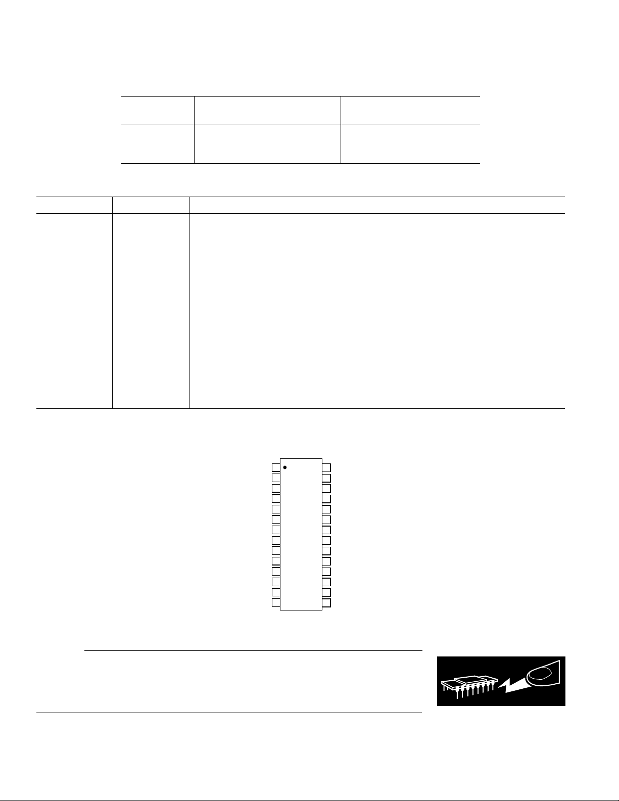
PIN CONNECTIONS
GND
1
V
2
D
VREF
3
OUT
VREF
4
IN
5
6
REF
BP
GND
AINB
GND
ENCODE
AD9049
7
TOP VIEW
8
V
(Not to Scale)
D
9
AIN D4
10
V
11
D
12
13
NC
14
NC = NO CONNECT
28
27
26
25
24
23
22
21
20
19
18
17
16
15
NC
D0 (LSB)
D1
D2
D3COMP
GND
V
DD
GND
V
DD
D5
D6
D7
D8 (MSB)
CAUTION
ESD (electrostatic discharge) sensitive device. Electrostatic charges as high as 4000 V readily
accumulate on the human body and test equipment and can discharge without detection.
Although the AD9049 features proprietary ESD protection circuitry, permanent damage may
occur on devices subjected to high energy electrostatic discharges. Therefore, proper ESD
precautions are recommended to avoid performance degradation or loss of functionality.
WARNING!
ESD SENSITIVE DEVICE
–4–
REV. A
 Loading...