

Monolithic 8-Bit
a
FEATURES
35 MSPS Encode Rate
16 pF Input Capacitance
550 mW Power Dissipation
Industry-Standard Pinouts
MIL-STD-883 Compliant Versions Available
APPLICATIONS
Professional Video Systems
Special Effects Generators
Electro-Optics
Digital Radio
Electronic Warfare (ECM, ECCM, ESM)
GENERAL DESCRIPTION
The AD9048 is an 8-bit, 35 MSPS flash converter, made on a
high speed bipolar process, which is an alternate source for the
TDC1048 unit, offers enhancements over its predecessor.
Lower power dissipation makes the AD9048 attractive for a
variety of system designs.
Because of its wide bandwidth, it is an ideal choice for real-time
conversion of video signals. Input bandwidth is flat with no
missing codes.
Clocked latching comparators, encoding logic and output buffer
registers operating at minimum rates of 35 MSPS preclude a
need for a sample-and-hold (S/H) or track-and-hold (T/H) in
most system designs using the AD9048. All digital control
inputs and outputs are TTL compatible.
Devices operating over two ambient temperature ranges and
with two grades of linearity are available. Linearities of either
0.5 LSB or 0.75 LSB can be ordered for a commercial range of
0°C to 70°C or extended case temperatures of –55°C to +125°C.
Video A/D Converter
AD9048
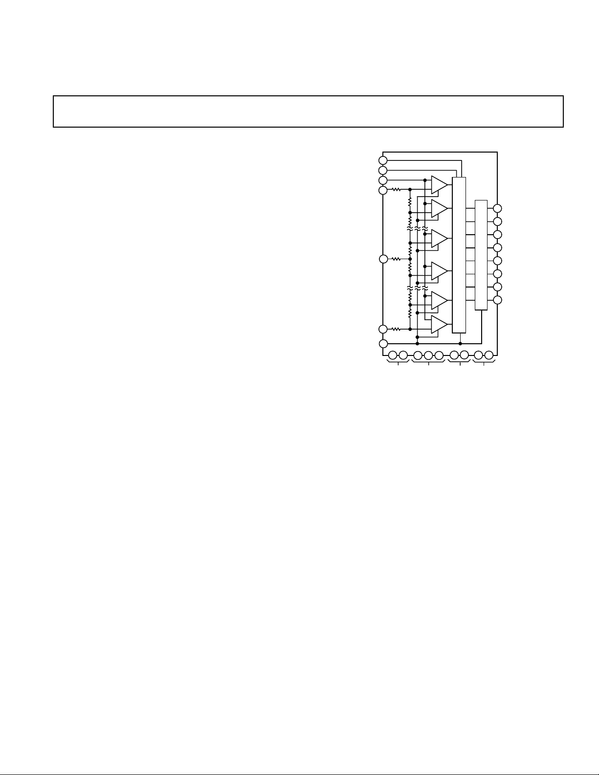
FUNCTIONAL BLOCK DIAGRAM
12
NLINV
28
NMINV
23
V
R
R
R
CONVERT
IN
18
T
R
R
R/2
27
M
R/2
R
R
26
B
17
6 10
V
CC
1
2
127
128
254
255
8 9
7
V
EE
Commercial versions are packaged in 28-lead DIPs; extended
temperature versions are available in ceramic DIP and ceramic
LCC packages. Both commercial units and MIL-STD-883 units
are standard products.
The AD9048 A/D converter is available in versions compliant
with MIL-STD-883. Refer to the Analog Devices Military Prod-
ucts Databook or current AD9048/883B data sheet for detailed
specifications.
AD9048
E
N
C
O
D
L
I
A
N
T
G
C
H
L
O
G
I
C
11
5
19
DGND AGND
25
1
2
3
4
13
14
15
16
D1 (MSB)
D2
D3
D3
D5
D6
D7
D8 (LSB)
REV. E
Information furnished by Analog Devices is believed to be accurate and
reliable. However, no responsibility is assumed by Analog Devices for its
use, nor for any infringements of patents or other rights of third parties that
may result from its use. No license is granted by implication or otherwise
under any patent or patent rights of Analog Devices.
One Technology Way, P.O. Box 9106, Norwood, MA 02062-9106, U.S.A.
Tel: 781/329-4700 www.analog.com
Fax: 781/326-8703 © Analog Devices, Inc., 2001

AD9048–SPECIFICATIONS
(typical with nominal supplies unless otherwise noted)
ABSOLUTE MAXIMUM RATINGS
VCC to DGND . . . . . . . . . . . . . . . . . . . –0.5 V dc to +7.0 V dc
AGND to DGND . . . . . . . . . . . . . . . . –0.5 V dc to +0.5 V dc
to AGND . . . . . . . . . . . . . . . . . . . +0.5 V dc to –7.0 V dc
V
EE
V
, VRT or VRB to AGND . . . . . . . . . . . . . . . . . . 0.5 V to V
IN
VRT to VRB . . . . . . . . . . . . . . . . . . . . . . –2.2 V dc to +2.2 V dc
CONV, NMINV or NLINV to DGND –0.5 V dc to +5.5 V dc
Applied Output Voltage to DGND . . –0.5 V dc to +5.5 V dc
Applied Output Current, Externally Forced
. . . . . . . . . . . . . . . . . . . . . . . . . . . . –1.0 mA to +6.0 mA
ELECTRICAL CHARACTERISTICS
Parameter (Conditions) Temp Level Min Typ Max Min Typ Max Min Typ Max Min Typ Max Unit
RESOLUTION 8 8 8 8 Bits
DC ACCURACY
Differential Nonlinearity 25°C I 0.4 0.75 0.3 0.5 0.4 0.75 0.3 0.5 LSB
Integral Nonlinearity 25°C I 0.6 0.75 0.4 0.5 0.6 0.75 0.4 0.5 LSB
No Missing Codes Full VI GUARANTEED GUARANTEED GUARANTEED GUARANTEED
INITIAL OFFSET ERROR
Top of Reference Ladder 25°CI 512 512 512 512mV
Bottom of Reference Ladder 25°CI 48 48 48 48 mV
Offset Drift Coefficient Full V 20 20 20 20 µV/°C
ANALOG INPUT
Input Voltage Range Full V –2.1; –2.1; –2.1; –2.1;
Input Bias Current
Input Resistance 25°C I 200 300 200 300 200 300 200 300 kΩ
Input Capacitance 25°C IV 1620 1620 1620 1620 pF
Full Power Bandwidth
REFERENCE INPUT
Positive Reference Voltage
Negative Reference Voltage
Differential Reference Voltage Full V 2.0 2.0 2.0 2.0 V
Reference Ladder Resistance Full VI 30 60 125 30 60 125 30 60 125 30 60 125 Ω
Ladder Temperature Coefficient Full V 0.22 0.22 0.22 0.22 Ω/°C
Reference Ladder Current Full VI 23 40 23 40 23 40 23 40 mA
Reference Input Bandwidth 25°C V 10 10 10 10 MHz
DYNAMIC PERFORMANCE
Conversion Rate 25°C I 35 38 35 38 35 38 35 38 MHz
Aperture Delay 25°C IV 2.4 5 2.4 5 2.4 5 2.4 5 ns
Aperture Uncertainty (Jitter) 25°C IV 2550 2550 2550 2550 ps
Output Delay (tPD)25°C I 13 15 9 15 9 15 9 15 ns
Output Hold Time (tOH)
Transient Response
Overvoltage Recovery Time
Rise Time 25°CI 9 9 9 9 ns
Fall Time 25°C I 14 14 14 14 ns
Output Time Skew
NMINV and NLINV INPUTS
0.4 V Input Current Full VI 200 200 200 200 µA
2.4 V Input Current Full VI 150 150 150 150 µA
5.5 V Input Current Full VI 150 150 150 150 µA
CONVERT INPUT
Logic “1” Voltage Full VI 2.0 2.0 2.0 2.0 V
Logic “0” Voltage Full VI 0.8 0.8 0.8 0.8 V
Logic “1” Current Full VI 150 150 150 150 µA
Logic “0” Current Full VI 500 500 500 500 µA
Input Capacitance 25°CIV4646 4646pF
Convert Pulsewidth (LOW) 25°C I 18 18 18 18 ns
Convert Pulsewidth (HIGH) 25°C I 10 10 10 10 ns
7
8
9
9
10
11
12
13
14
1
Output Short-Circuit Duration . . . . . . . . . . . . . . . . . 1.0 sec
5
Operating Temperature Range (Ambient)
AD9048JJ/KJ/JQ/KQ . . . . . . . . . . . . . . . . . . . . 0°C to 70°C
EE
2
AD9048SE/SQ/TE/TQ . . . . . . . . . . . . . . –55°C to +125°C
Maximum Junction Temperature (Plastic) . . . . . . . . . 150°C
Maximum Junction Temperature (Hermetic) . . . . . . . 150°C
Lead Temperature (Soldering, 10 sec) . . . . . . . . . . . . 300°C
6
6
Storage Temperature Range . . . . . . . . . . . . –65°C to +150°C
3, 4
(VCC = +5.0 V; VEE = –5.2 V; Differential Reference Voltage = 2.0 V, unless otherwise noted)
Test AD9048JJ/JQ AD9048KJ/KQ AD9048SE/SQ AD9048TE/TQ
Full VI 1.0 0.75 1.0 0.75 LSB
Full VI 1.0 0.75 1.0 0.75 LSB
Full VI 12 12 12 12 mV
Full VI 8 8 8 8 mV
25°C I 36 60 36 60 36 60 36 60 µA
Full VI 100 100 100 100 µA
Full VI 40 40 40 40 kΩ
25°CIV1015101510151015MHz
Full V 0.0 0.0 0.0 0.0 V
Full V –2.0 –2.0 –2.0 –2.0 V
25°CI 58 58 58 58 ns
25°C IV 6 20 6 20 6 20 6 20 ns
25°CV88 88ns
25°C I 4.5 7 4.5 7 4.5 7 4.5 7 ns
+0.1 +0.1 +0.1 +0.1 V
–2–
REV. E

AD9048
Parameter (Conditions) Temp Level Min Typ Max Min Typ Max Min Typ Max Min Typ Max Unit
Test AD9048JJ/JQ AD9048KJ/KQ AD9048SE/SQ AD9048TE/TQ
AC LINEARITY
In-Band Harmonics
dc to 2.438 MHz
dc to 9.35 MHz
Signal-to-Noise Ratio (SNR)
15
16
15
25°C I 47 50 49 55 47 50 49 55 dBc
25°C V 48 48 48 48 dBc
1.248 MHz Input Frequency1725°C I 43.5 44 45 46 43.5 44 45 46 dB
2.438 MHz Input Frequency1725°C I 43 44 44 46 43 44 44 46 dB
1.248 MHz Input Frequency1825°C I 52.5 53 54 55 52.5 53 54 55 dB
2.438 MHz Input Frequency1825°C I 52 53 53 55 52 53 53 55 dB
Signal-to-Noise Ratio (SNR)
1.248 MHz Input Frequency1725°C I 43.5 44 45 46 43.5 44 45 46 dB
9.35 MHz Input Frequency
Noise Power Ratio (NPR)
Differential Phase
Differential Gain
20
20
16
17
19
25°C V 40.5 40.5 40.5 40.5 dB
25°C IV 36.5 39 36.5 39 36.5 39 36.5 39 dB
25°C IV 1 1 1 1 Degree
25°CIV 2 2 2 2 %
DIGITAL OUTPUTS
Logic “1” Voltage Full VI 2.4 2.4 2.4 2.4 V
Logic “0” Voltage Full VI 0.5 0.5 0.5 0.5 V
Short Circuit Current
5
Full VI 30 30 30 30 mA
POWER SUPPLY
Positive Supply Current 25°C I 34 56 34 56 34 56 34 56 mA
Full VI 58 58 58 58 mA
Negative Supply Current 25°C I 90 110 90 110 90 110 90 110 mA
Full VI 120 120 120 120 mA
Nominal Power Dissipation 25°C V 550 550 550 550 mW
Reference Ladder Dissipation 25°C V 45 45 45 45 mW
NOTES
1
Maximum ratings are limiting values to be applied individually, and beyond which
the serviceability of the device may be impaired. Functional operation under any of
these conditions is not necessarily implied. Exposure to absolute maximum rating
conditions for extended periods of time may affect device reliability.
2
Applied voltage must be current-limited to specified range.
3
Forcing voltage must be limited to specified range.
4
Current is specified as negative when flowing into the device.
5
Output High; one pin to ground; one second duration.
6
Typical thermal impedances (no air flow) are as follows:
Ceramic DIP: θJA = 49°C/W;
JLCC: θJA = 59°C/W; θJC = 19°C/W.
θJC = 15°C/W, LCC: θJA = 69°C/W;
θ
= 21°C/W,
JC
To calculate junction temperature (TJ), use power dissipation (PD) and thermal
impedance: TJ = PD (θJA) + T
7
Measured with VIN = 0 V and CONVERT low (sampling mode).
8
Determined by beat frequency testing for no missing codes.
9
VRT ≥ VRB under all circumstances.
= PD (θJC) = + T
AMBIENT
CASE
.
10
Outputs terminated with 40 pF and eight 10 Ω pull-up resistors.
11
Interval from 50% point of leading edge CONVERT pulse to change in
output data.
12
For full-scale step input, 8-bit accuracy attained in specified time.
13
Recovers to 8-bit accuracy in specified time after –3 V input overvoltage.
14
Output time skew includes high-to-low and low-to-high transitions as well as
bit-to-bit time skew differences.
15
Measured at 20 MHz encode rate with analog input 1 dB below full scale.
16
Measured at 35 MHz encode rate with analog input 1 dB below full scale.
17
RMS signal to rms noise.
18
Peak signal to rms noise.
19
DC to 8 MHz noise bandwidth with 1.248 MHz slot; four sigma loading;
20 MHz encode.
20
Clock frequency = 4 × NTSC = 14.32 MHz. Measured with 40-IRE
modulated ramp.
Specifications subject to change without notice.
EXPLANATION OF TEST LEVELS
Test Level I – 100% production tested.
Test Level II – 100% production tested at 25°C and
sample tested at specific temperatures.
Test Level III – Sample tested only.
Test Level IV – Parameter is guaranteed by design and
characterization testing.
Test Level V – Parameter is a typical value only.
Test Level VI – All devices are 100% production tested at
25°C. 100% production tested at temperature
extremes for military temperature devices;
sample tested at temperature extremes for
commercial/industrial devices.
REV. E
–3–

AD9048
14
13
12
11
10
9
8
1
2
3
4
7
6
5
17
16
15
20
19
18
28
27
26
25
24
23
22
21
TOP VIEW
(Not to Scale)
AD9048
NC = NO CONNECT
NMINV
R
M
R
B
AGND
NC
V
IN
NC
NC
NC
AGND
R
T
CONVERT
D8 (LSB)
D7
(MSB) D1
D2
D3
D4
DGND
V
CC
V
EE
V
EE
V
EE
V
CC
DGND
NLINV
D5
D6
WARNING!
ESD SENSITIVE DEVICE
ORDERING GUIDE
Package
Model Linearity Temperature Option
1
PIN CONFIGURATIONS
DIP (D Package)
AD9048JJ 0.75 LSB 0°C to 70°C J-28A
AD9048KJ 0.5 LSB 0°C to 70°C J-28A
AD9048JQ 0.75 LSB 0°C to 70°C D-28
AD9048KQ 0.5 LSB 0°C to 70°C D-28
AD9048SE
AD9048TE
AD9048SQ
2
0.75 LSB –55°C to +125°C E-28A
2
0.5 LSB –55°C to +125°C E-28A
2
0.75 LSB –55°C to +125°C D-28
AD9048TQ20.5 LSB –55°C to +125°C D-28
NOTES
1
E = Leadless Ceramic Chip Carrier; J = J-Leaded Ceramic; D = Cerdip.
2
For temperature designation only. MIL-STD-883 and Standard Military
Drawing available.
MECHANICAL INFORMATION
Die Dimensions . . . . . . . . . . . . . . . . 140 × 137 × 21 (± 2) mils
Pad Dimensions . . . . . . . . . . . . . . . . . . . . . . . . . . . . 4 × 4 mils
LCC (E Package)
Metalization . . . . . . . . . . . . . . . . . . . . . . . . . . . . . . . . . . . Gold
Backing . . . . . . . . . . . . . . . . . . . . . . . . . . . . . . . . . . . . . None
Substrate Potential . . . . . . . . . . . . . . . . . . . . . . . . . . . . . . V
Passivation . . . . . . . . . . . . . . . . . . . . . . . . . . . . . . . . . . Nitride
Die Attach . . . . . . . . . . . . . . . . . . . . . . . . . . . . . Gold Eutectic
Bond Wire . . . . . . . . . . . . . . . . 1 mil Gold; Gold Ball Bonding
AGND AIN AGND
RLOW
RMID
NMINV
MSB
D2
D3
D4
DGND
V
V
CC
V
CC
VEEV
EE
VCCV
EE
CC
RTOP
CONV
D8
D7
D6
D5
NLINV
DGND
DGND
Figure 1. Bonding Diagram
CAUTION
ESD (electrostatic discharge) sensitive device. Electrostatic charges as high as 4000 V readily
accumulate on the human body and test equipment and can discharge without detection.
Although the AD9048 features proprietary ESD protection circuitry, permanent damage may
occur on devices subjected to high-energy electrostatic discharges. Therefore, proper ESD
precautions are recommended to avoid performance degradation or loss of functionality.
EE
–4–
DGND
V
CC
V
EE
V
EE
V
EE
V
CC
DGND
J-Leaded Ceramic (J Package)
R
R
NMINV
(MSB) D1
D2
D3
D4
D4
5
6
7
8
9
10
11
12
NLINV
NC = NO CONNECT
AGND
26
B
27
M
28
1
2
3
4
DGND
NC = NO CONNECT
13 14 15 16 17 18
B
M
R
D3
D2
3426
2
AD9048
TOP VIEW
(Not to Scale)
D5
D6
IN
V
NC
AD9048
TOP VIEW
TOP VIEW
(Not to Scale)
(Not to Scale)
CC
VEEVEEV
V
NMINV
D1 (MSB)
28 271
D7
(LSB) D8
NC
NC
EE
R
T
R
CONVERT
NC
AGND
1921 2025 24 2223
115106789
CC
V
DGND
25
AGND
24
NC
23
V
22
NC
21
NC
20
NC
19
AGND
18
R
T
17
CONVERT
16
D8 (LSB)
15
D7
14
D6
13
D5
12
NLINV
IN
REV. E

PIN FUNCTION DESCRIPTIONS
AD9048
Pin Description
D1–D8 Eight digital outputs. D1 (MSB) is the most
significant bit of the digital output word;
D8 (LSB) is the least significant bit.
AGND One of two analog ground returns. Both
grounds should be connected together and to
low impedance ground plane near the AD9048.
DGND One of two digital ground returns. Both
grounds should be connected together and to
low impedance ground plane near the AD9048.
V
CC
V
EE
Positive supply terminals; nominally +5.0 V.
Negative supply terminals; nominally –5.2 V.
CONVERT Input for conversion signal; sample of analog
input signal taken on rising edge of this pulse.
–5.2V
0.1F
V
EE
V
IN
CONVERT
AD9048
R
B
R
T
DIGITAL
GROUND
AD1
AD2
–2.0V
100
510
Pin Description
R
B
Most negative reference voltage for internal
reference ladder.
R
M
R
T
Midpoint tap on internal reference ladder.
Most positive reference voltage for internal
reference ladder.
V
IN
Analog input signal pin.
NMINV “Not Most Significant Bit Invert.” In normal
operation, this pin floats high; logic LOW at
NMINV inverts most significant bit of digital
output word [D1 (MSB)].
NLINV “Not Least Significant Bit Invert.” In normal
operation, this pin floats high; logic LOW at
NLINV inverts the seven least significant bits
of the digital output word.
+5.0V
V
CC
(MSB) D1
(LSB) D8
ANALOG
GROUND
D2
D3
D4
D5
D6
D7
1k
LOAD
RESISTORS
0.1F
ALL RESISTORS 5%
ALL CAPACITORS 20%
ALL SUPPLY VOLTAGES 5%
AD1
AD2
5s
OPTION #1 (STATIC): AD1 = –2.0V; AD2 = +2.4V
OPTION #2 (DYNAMIC): SEE WAVEFORMS
640s
Figure 2. Burn-In Diagram
0V
–2.0V
V
IH
V
IL
–5–REV. E

AD9048
THEORY OF OPERATION
Refer to the Functional Block Diagram of the AD9048. The
AD9048 comprises three functional sections: a comparator
array, encoding logic and output latches.
Within the array, the analog input signal to be digitized is
compared with 255 reference voltages. The outputs of all comparators whose references are below the input signal level will be
high; outputs whose references are above that level will be low.
The n-of-255 code that results from this comparison is applied
to the encoding logic where it is converted into binary coding.
When it is inverted with dc signals applied to the NLINV and/or
NMINV pins, it becomes two’s complement.
After encoding, the signal is applied to the output latch circuits
where it is held constant between updates controlled by the
application of CONVERT pulses.
The AD9048 uses strobed latching comparators in which comparator outputs are either high or low, as dictated by the analog
input level. Data appearing at the output pins have a pipeline
delay of one encode cycle.
Input signal levels between the references applied to R
(Pin 26) will appear at the output as binary numbers
and R
B
(Pin 18)
T
between 0 and 255, inclusive. Signals outside that range will
show up as either full-scale positive or full-scale negative outputs. No damage will occur to the AD9048 as long as the input
is within the voltage range of V
to +0.5 V.
EE
The significantly reduced input capacitance of the AD9048
lowers the drive requirements of the input buffer/amplifier and
also induces much smaller phase shift in the analog input signal.
Applications that depend on controlled phase shift at the converter input can benefit from using the AD9048 because of its
inherently lower phase shift.
The CONVERT, analog input and digital output circuits are
shown in Figure 3.
System timing, which provides details on delays through the
AD9048 as well as the relationships of various timing events, is
shown in Figure 4.
N+1
ANALOG
INPUT
CONVERT
OUTPUT
DATA
N
t
PD
APERTURE
DELAY
t
OH
N– 1
DATA
CHANGING
N
N+2
DATA
CHANGING
N+1
Figure 4. Timing Diagram
Dynamic performance of the AD9048, i.e., typical signal-tonoise ratio, is illustrated in Figures 3 and 4.
50
48
46
44
42
SIGNAL-TO-NOISE RATIO – dB
40
38
ANALOG INPUT FREQUENCY – 1dB BELOW FULL-SCALE
10MHz1MHz100kHz
Figure 5. Dynamic Performance (20 MHz Encode Rate)
CONVERT
ANALOG
INPUT
5.0V
13k
–5.2V
–5.2V
5.0V
–5.2V
–5.2V
COMPARATOR CELLS
Figure 3. Input/Output Circuits
DIGITAL
OUTPUTS
R
R/2
R/2
R
50
48
46
44
R
T
42
SIGNAL-TO-NOISE RATIO – dB
40
R
M
38
ANALOG INPUT FREQUENCY – 1dB BELOW FULL-SCALE
10MHz1MHz100kHz
Figure 6. Dynamic Performance (35 MHz Encode Rate)
R
B
–6–
REV. E

LAYOUT SUGGESTIONS
0.1F
V
EE
V
CC
+5.0V
–5.2V
V
IN
R
T
R
B
CONVERT
43
AD9048
R
R
50
1k
100
2N3906
AD741
5
1k
0.1F
0.1F
2k
27
0.1F
–5.2V
0.1F
ANALOG
INPUT
(0V TO 2V)
TTL
CONVERT
SIGNAL
D1 (MSB)
D8 (LSB)
10k
AD589
AD9617/AD9618,
AD9620/AD9630,
AD847
Designs that use the AD9048 or any other high speed device
must follow some basic layout rules to ensure optimum
performance.
The first requirement is to have a large, low impedance ground
plane under and around the converter. If the system uses separate
analog and digital grounds, both should be solidly connected
together, and to the ground plane, as closely to the AD9048 as
practical to avoid ground loop currents.
Ceramic 0.1 µF decoupling capacitors should be placed as closely
as possible to the supply pins of the AD9048. For decoupling
low frequency signals, use 10 µF tantalum capacitors, also con-
nected as closely as practical to voltage supply pins.
Within the AD9048, reference currents may vary because of
coupling between the clock and input signals. As a result, it is
important that the ends of the reference ladder, R
(Pin 28), be connected to low impedances (as measured
R
B
(Pin 18) and
T
from ground).
If the AD9048 is being used in a circuit in which the reference
is not varied, a bypass capacitor to ground is strongly recommended. In applications that use varying references, they must
be driven from a low impedance source.
AD9048
Figure 7. Typical Connections
Table I. Truth Table
Offset Two’s
Binary Complement
Step Range True Inverted True Inverted
–2.000 V FS –2.0480 V FS NMINV = 1 0 0 1
7.8431 mV Step 8.000 mV Step NLINV = 1 0 1 0
000 0.0000 V 0.0000 V 00000000 11111111 10000000 01111111
001 –0.0078 V –0.0080 V 00000001 11111110 10000001 01111110
•• • • • • •
•• • • • • •
•• • • • • •
127 –0.9961 V –1.0160 V 01111111 10000000 11111111 00000000
128 –1.0039 V –1.0240 V 10000000 01111111 00000000 11111111
129 –1.0118 V –1.0320 V 10000001 01111110 00000001 11111110
•• • • • • •
•• • • • • •
•• • • • • •
254 –1.9921 V –2.0320 V 11111110 00000001 01111110 10000001
255 –2.0000 V –2.0400 V 11111111 00000000 01111111 10000000
–7–REV. E

AD9048
(
)
OUTLINE DIMENSIONS
Dimensions shown in inches and (mm).
0.005 (0.13) MIN
PIN 1
0.225
(5.72)
MAX
0.200 (5.08)
0.125 (3.18)
28-Lead Ceramic Side-Brazed DIP
0.100 (2.54) MAX
28
114
1.490 (37.85) MAX
0.026 (0.66)
0.014 (0.36)
0.100 (2.54)
BSC
15
0.070 (1.78)
0.030 (0.76)
BOTTOM VIEW
0.022 ±0.003
(0.559 ±0.076)
0.610 (15.49)
0.500 (12.70)
0.015
(0.38)
MIN
0.150
(3.81)
MIN
SEATING
PLANE
0.620 (15.75)
0.590 (14.99)
15°
0°
0.050
(1.27)
BSC
0.458 (11.63)
0.442 (11.23)
SQ
0.018 (0.46)
0.008 (0.20)
NOTES:
1
THIS DIMENSION CONTROLS THE OVERALL PACKAGE THICKNESS
APPLIES TO ALL FOUR SIDES
ALL TERMINALS ARE GOLD PLATED
28-Lead J-Lead Package
0.450 ±0.006
(11.43 ±0.152)
25 19
26
PIN 1
(PINS DOWN)
4
5
0.488 ±0.010
(11.43 ±0.254)
TOP VIEW
SQ
SQ
18
0.300
(7.62)
TYP
12
11
28-Terminal Leadless Chip Carrier
0.050 ±0.005
0.171 (4.34)
MAX
1
(1.27 ±0.13)
0.040 (1.02) x 45
REF 3 PLCS
0.039 ±0.005
(0.991 ±0.127)
0.028 ±0.002
(0.711 ±0.051)
0.019 ±0.002
(0.483 ±0.051)
0.006 ±0.0006
(0.152 ±0.015)
0.055 (1.40)
0.045 (1.14)
18
19
12
11
0.420 ±0.010
(10.668 ±0.254)
BOTTOM
VIEW
0.075 (1.91) REF
26
25
28
1
5
4
0.020 (0.51) x 45
REF 1 PLC
0.100 (2.54)
0.064 (1.63)
0.102 ±0.010
1.448 ±0.254
0.028 (0.71)
0.022 (0.56)
NO 1
PIN INDEX
C00555a–0–9/01(E)
Revision History
Location Page
09/01—Data Sheet changed from REV. D to REV. E.
Change in ABSOLUTE MAXIMUM RATINGS . . . . . . . . . . . . . . . . . . . . . . . . . . . . . . . . . . . . . . . . . . . . . . . . . . . . . . . . . . . . . . . 2
05/01—Data Sheet changed from REV. C to REV. D.
Change in ORDERING GUIDE and PIN DESIGNATIONS . . . . . . . . . . . . . . . . . . . . . . . . . . . . . . . . . . . . . . . . . . . . . . . . . . . . . 4
Edits to 28-Lead Ceramic Side-Brazed DIP Package . . . . . . . . . . . . . . . . . . . . . . . . . . . . . . . . . . . . . . . . . . . . . . . . . . . . . . . . . . . . . 8
–8–
REV. E
PRINTED IN U.S.A.
 Loading...