Analog Devices AD9048 Datasheet

Monolithic 8-Bit
1
R
2
127
R
R/2
R/2
128
R
254
255
R
E
N
C
O
D
I
N
G
L
O
G
I
C
13
14
15
16
1
2
3
4
28
23
18
12
27
26
17
19 256 10
7
8 9
11
5
L
A
T
C
H
V
CC
V
EE
DGND AGND
D1 (MSB)
D2
D3
D3
D5
D6
D7
D8 (LSB)
NLINV
NMINV
V
IN
R
T
R
M
R
B
CONVERT
AD9048
a
FEATURES
35 MSPS Encode Rate
16 pF Input Capacitance
550 mW Power Dissipation
Industry-Standard Pinouts
MIL-STD-883 Compliant Versions Available
APPLICATIONS
Professional Video Systems
Special Effects Generators
Electro-Optics
Digital Radio
Electronic Warfare (ECM, ECCM, ESM)
GENERAL DESCRIPTION
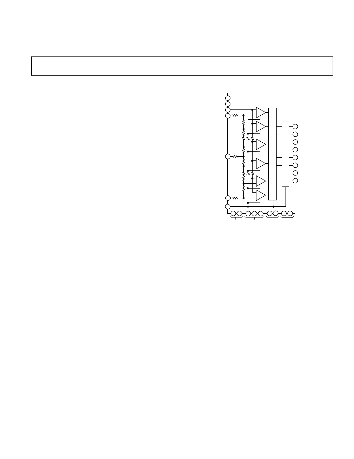
The AD9048 is an 8-bit, 35 MSPS flash converter, made on a
high speed bipolar process, which is an alternate source for the
TDC1048 unit, offers enhancements over its predecessor.
Lower power dissipation makes the AD9048 attractive for a
variety of system designs.
Because of its wide bandwidth, it is an ideal choice for real-time
conversion of video signals. Input bandwidth is flat with no
missing codes.
Clocked latching comparators, encoding logic and output buffer
registers operating at minimum rates of 35 MSPS preclude a
need for a sample-and-hold (S/H) or track-and-hold (T/H) in
most system designs using the AD9048. All digital control inputs and outputs are TTL compatible.
Devices operating over two ambient temperature ranges and
with two grades of linearity are available. Linearities of either
0.5 LSB or 0.75 LSB can be ordered for a commercial range
of 0°C to +70°C or extended case temperatures of –55°C to
+125°C.
Video A/D Converter
AD9048
FUNCTIONAL BLOCK DIAGRAM
Commercial versions are packaged in 28-lead DIPs; extended
temperature versions are available in ceramic DIP and ceramic
LCC packages. Both commercial units and MIL-STD-883 units
are standard products.
The AD9048 A/D converter is available in versions compliant
with MIL-STD-883. Refer to the Analog Devices Military Prod-
ucts Databook or current AD9048/883B data sheet for detailed
specifications.
REV. C
Information furnished by Analog Devices is believed to be accurate and
reliable. However, no responsibility is assumed by Analog Devices for its
use, nor for any infringements of patents or other rights of third parties
which may result from its use. No license is granted by implication or
otherwise under any patent or patent rights of Analog Devices.
One Technology Way, P.O. Box 9106, Norwood, MA 02062-9106, U.S.A.
Tel: 781/329-4700 World Wide Web Site: http://www.analog.com
Fax: 781/326-8703 © Analog Devices, Inc., 1999

AD9048–SPECIFICATIONS
ABSOLUTE MAXIMUM RATINGS
1
(typical with nominal supplies unless otherwise noted)
VCC to DGND . . . . . . . . . . . . . . . . . . . –0.5 V dc to +7.0 V dc
AGND to DGND . . . . . . . . . . . . . . . . –0.5 V dc to +0.5 V dc
to AGND . . . . . . . . . . . . . . . . . . . +0.5 V dc to –7.0 V dc
V
EE
, VRT or VRB to AGND . . . . . . . . . . . . . . . . . +0.5 V to V
V
IN
EE
VRT to VRB . . . . . . . . . . . . . . . . . . . . . . –2.2 V dc to +2.2 V dc
CONV, NMINV or NLINV to DGND –0.5 V dc to +5.5 V dc
Applied Output Voltage to DGND . . . –0.5 V dc to +5.5 V dc
Applied Output Current, Externally Forced
. . . . . . . . . . . . . . . . . . . . . . . . . . . . . –1.0 mA to +6.0 mA
2
3, 4
Output Short-Circuit Duration . . . . . . . . . . . . . . . . . . 1.0 sec
Operating Temperature Range (Ambient)
AD9048JJ/KJ/JQ/KQ . . . . . . . . . . . . . . . . . . . 0°C to +70°C
AD9048SE/SQ/TE/TQ . . . . . . . . . . . . . . –55°C to +125°C
Maximum Junction Temperature (Plastic) . . . . . . . . +150°C
Maximum Junction Temperature (Hermetic) . . . . . . +175°C
Lead Temperature (Soldering, 10 sec) . . . . . . . . . . . .+300°C
Storage Temperature Range . . . . . . . . . . . . –65°C to +150°C
5
6
6
ELECTRICAL CHARACTERISTICS
Parameter (Conditions) Temp Level Min Typ Max Min Typ Max Min Typ Max Min Typ Max Units
RESOLUTION 8 8 8 8 Bits
DC ACCURACY
Differential Nonlinearity +25°C I 0.4 0.75 0.3 0.5 0.4 0.75 0.3 0.5 LSB
Integral Nonlinearity +25°C I 0.6 0.75 0.4 0.5 0.6 0.75 0.4 0.5 LSB
No Missing Codes Full VI GUARANTEED GUARANTEED GUARANTEED GUARANTEED
INITIAL OFFSET ERROR
Top of Reference Ladder +25°CI 512 512 512 512mV
Bottom of Reference Ladder +25°CI 48 48 48 48 mV
Offset Drift Coefficient Full V 20 20 20 20 µV/°C
ANALOG INPUT
Input Voltage Range Full V –2.1; –2.1; –2.1; –2.1;
Input Bias Current
Input Resistance +25°C I 200 300 200 300 200 300 200 300 kΩ
Input Capacitance +25°CIV 1620 1620 1620 1620 pF
Full Power Bandwidth
REFERENCE INPUT
Positive Reference Voltage
Negative Reference Voltage
Differential Reference Voltage Full V 2.0 2.0 2.0 2.0 V
Reference Ladder Resistance Full VI 30 60 125 30 60 125 30 60 125 30 60 125 Ω
Ladder Temperature Coefficient Full V 0.22 0.22 0.22 0.22 Ω/°C
Reference Ladder Current Full VI 23 40 23 40 23 40 23 40 mA
Reference Input Bandwidth +25°C V 10 10 10 10 MHz
DYNAMIC PERFORMANCE
Conversion Rate +25°C I 35 38 35 38 35 38 35 38 MHz
Aperture Delay +25°C IV 2.4 5 2.4 5 2.4 5 2.4 5 ns
Aperture Uncertainty (Jitter) +25°CIV 2550 2550 2550 2550 ps
Output Delay (t
Output Hold Time (tOH)
Transient Response
Overvoltage Recovery Time
Rise Time +25°CI 9 9 9 9 ns
Fall Time +25°C I 14 14 14 14 ns
Output Time Skew
NMINV and NLINV INPUTS
+0.4 V Input Current Full VI 200 200 200 200 µA
+2.4 V Input Current Full VI 150 150 150 150 µA
+5.5 V Input Current Full VI 150 150 150 150 µA
CONVERT INPUT
Logic “1” Voltage Full VI 2.0 2.0 2.0 2.0 V
Logic “0” Voltage Full VI 0.8 0.8 0.8 0.8 V
Logic “1” Current Full VI 150 150 150 150 µA
Logic “0” Current Full VI 500 500 500 500 µA
Input Capacitance +25°CIV4646 4646pF
Convert Pulsewidth (LOW) +25°C I 18 18 18 18 ns
Convert Pulsewidth (HIGH) +25°C I 10 10 10 10 ns
7
8
9
) +25°C I 13 15 9 15 9 15 9 15 ns
PD
11
12
14
Full VI 1.0 0.75 1.0 0.75 LSB
Full VI 1.0 0.75 1.0 0.75 LSB
Full VI 12 12 12 12 mV
Full VI 8 8 8 8 mV
+25°C I 36 60 36 60 36 60 36 60 µA
Full VI 100 100 100 100 µA
Full VI 40 40 40 40 kΩ
+25°CIV1015101510151015MHz
Full V 0.0 0.0 0.0 0.0 V
9
Full V –2.0 –2.0 –2.0 –2.0 V
10
+25°CI 58 58 58 58 ns
+25°C IV 6 20 6 20 6 20 6 20 ns
13
+25°CV88 88ns
+25°C I 4.5 7 4.5 7 4.5 7 4.5 7 ns
(VCC = +5.0 V; VEE = –5.2 V; Differential Reference Voltage = 2.0 V, unless otherwise noted)
Test AD9048JJ/JQ AD9048KJ/KQ AD9048SE/SQ AD9048TE/TQ
+0.1 +0.1 +0.1 +0.1 V
REV. C–2–

AD9048
Parameter (Conditions) Temp Level Min Typ Max Min Typ Max Min Typ Max Min Typ Max Units
Test AD9048JJ/JQ AD9048KJ/KQ AD9048SE/SQ AD9048TE/TQ
AC LINEARITY
In-Band Harmonics
dc to 2.438 MHz
dc to 9.35 MHz
Signal-to-Noise Ratio (SNR)
1.248 MHz Input Frequency
2.438 MHz Input Frequency
1.248 MHz Input Frequency
2.438 MHz Input Frequency
Signal-to-Noise Ratio (SNR)
1.248 MHz Input Frequency
9.35 MHz Input Frequency
Noise Power Ratio (NPR)
Differential Phase
Differential Gain
15
16
15
16
17
19
20
20
+25°C I 47 50 49 55 47 50 49 55 dBc
+25°C V 48 48 48 48 dBc
17
+25°C I 43.5 44 45 46 43.5 44 45 46 dB
17
+25°C I 43 44 44 46 43 44 44 46 dB
18
+25°C I 52.5 53 54 55 52.5 53 54 55 dB
18
+25°C I 52 53 53 55 52 53 53 55 dB
17
+25°C I 43.5 44 45 46 43.5 44 45 46 dB
+25°C V 40.5 40.5 40.5 40.5 dB
+25°C IV 36.5 39 36.5 39 36.5 39 36.5 39 dB
+25°C IV 1 1 1 1 Degree
+25°CIV 2 2 2 2 %
DIGITAL OUTPUTS
Logic “1” Voltage Full VI 2.4 2.4 2.4 2.4 V
Logic “0” Voltage Full VI 0.5 0.5 0.5 0.5 V
Short Circuit Current
5
Full VI 30 30 30 30 mA
POWER SUPPLY
Positive Supply Current +25°C I 34 56 34 56 34 56 34 56 mA
Full VI 58 58 58 58 mA
Negative Supply Current +25°C I 90 110 90 110 90 110 90 110 mA
Full VI 120 120 120 120 mA
Nominal Power Dissipation +25°C V 550 550 550 550 mW
Reference Ladder Dissipation +25°C V 45 45 45 45 mW
NOTES
1
Maximum ratings are limiting values to be applied individually, and beyond which
the serviceability of the device may be impaired. Functional operation under any of
these conditions is not necessarily implied. Exposure to absolute maximum rating
conditions for extended periods of time may affect device reliability.
2
Applied voltage must be current-limited to specified range.
3
Forcing voltage must be limited to specified range.
4
Current is specified as negative when flowing into the device.
5
Output High; one pin to ground; one second duration.
6
Typical thermal impedances (no air flow) are as follows:
Ceramic DIP: θJA = 49°C/W; θJC = 15°C/W LCC: θJA = 69°C/W; θ
JLCC: θJA = 59°C/W; θJC = 19°C/W
= 21°C/W
JC
To calculate junction temperature (TJ), use power dissipation (PD) and thermal
impedance: T
7
Measured with VIN = 0 V and CONVERT low (sampling mode).
8
Determined by beat frequency testing for no missing codes.
9
V
≥ V
RT
= PD (θ
J
under all circumstances.
RB
) + T
JA
AMBIENT
= PD (θ
) = + T
JC
CASE.
10
Outputs terminated with 40 pF and eight 10 Ω pull-up resistors.
11
Interval from 50% point of leading edge CONVERT pulse to change in output
data.
12
For full-scale step input, 8-bit accuracy attained in specified time.
13
Recovers to 8-bit accuracy in specified time after –3 V input overvoltage.
14
Output time skew includes high-to-low and low-to-high transitions as well as
bit-to-bit time skew differences.
15
Measured at 20 MHz encode rate with analog input 1 dB below full scale.
16
Measured at 35 MHz encode rate with analog input 1 dB below full scale.
17
RMS signal to rms noise.
18
Peak signal to rms noise.
19
DC to 8 MHz noise bandwidth with 1.248 MHz slot; four sigma loading;
20 MHz encode.
20
Clock frequency = 4 × NTSC = 14.32 MHz. Measured with 40-IRE
modulated ramp.
Specifications subject to change without notice.
EXPLANATION OF TEST LEVELS
Test Level I – 100% production tested.
Test Level II – 100% production tested at +25°C and
sample tested at specific temperatures.
Test Level III – Sample tested only.
Test Level IV – Parameter is guaranteed by design and
characterization testing.
REV. C
Test Level V – Parameter is a typical value only.
Test Level VI – All devices are 100% production tested at
+25°C. 100% production tested at tempera-
ture extremes for military temperature devices; sample tested at temperature extremes
for commercial/industrial devices.
–3–
 Loading...