Analog Devices AD8802ARU, AD8802AR, AD8802AN, AD8804ARU, AD8804AR Datasheet
...
12 Channel, 8-Bit TrimDACs
a
FEATURES
Low Cost
Replaces 12 Potentiometers
Individually Programmable Outputs
3-Wire SPI Compatible Serial Input
Power Shutdown <55 mWatts Including I
Midscale Preset, AD8802
Separate V
Range Setting, AD8804
REFL
+3 V to +5 V Single Supply Operation
APPLICATIONS
Automatic Adjustment
Trimmer Replacement
Video and Audio Equipment Gain and Offset Adjustment
Portable and Battery Operated Equipment
GENERAL DESCRIPTION
The 12-channel AD8802/AD8804 provides independent digitallycontrollable voltage outputs in a compact 20-lead package. This
potentiometer divider TrimDAC® allows replacement of the
mechanical trimmer function in new designs. The AD8802/
AD8804 is ideal for dc voltage adjustment applications.
Easily programmed by serial interfaced microcontroller ports,
the AD8802 with its midscale preset is ideal for potentiometer
replacement where adjustments start at a nominal value. Applications such as gain control of video amplifiers, voltage controlled frequencies and bandwidths in video equipment,
geometric correction and automatic adjustment in CRT computer graphic displays are a few of the many applications ideally
suited for these parts. The AD8804 provides independent control of both the top and bottom end of the potentiometer divider
allowing a separate zero-scale voltage setting determined by the
pin. This is helpful for maximizing the resolution of
V
REFL
devices with a limited allowable voltage control range.
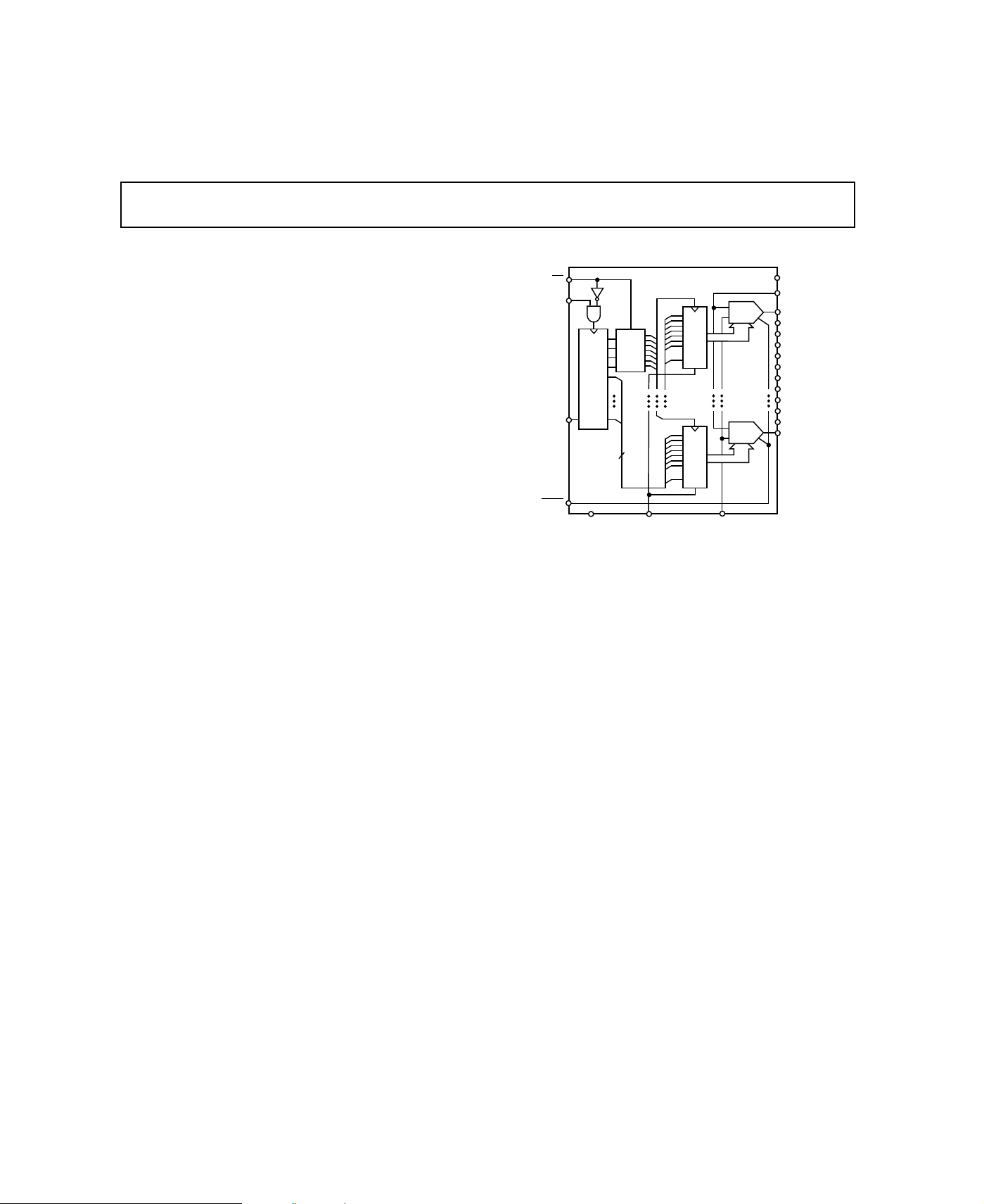
Internally the AD8802/AD8804 contains 12 voltage-output
digital-to-analog converters, sharing a common referencevoltage input.
TrimDAC is a registered trademark of Analog Devices, Inc.
DD
& I
REF
with Power Shutdown
AD8802/AD8804
FUNCTIONAL BLOCK DIAGRAM
CS
CLK
SDI
SHDN
D11
D10
D9
D8
D7
SER
REG
DD0
GND
AD8802/AD8804
EN
ADDR
DEC
8
RS
(AD8802 ONLY)
D7
DAC
REG
#1
D0
R
D7
DAC
REG
#12
D0
R
(AD8804 ONLY)
V
REFL
DAC
DAC
12
1
Each DAC has its own DAC latch that holds its output state.
These DAC latches are updated from an internal serial-toparallel shift register that is loaded from a standard 3-wire
serial input digital interface. The serial-data-input word is
decoded where the first 4 bits determine the address of the DAC
latches to be loaded with the last 8 bits of data. The AD8802/
AD8804 consumes only 10 µA from 5 V power supplies. In ad-
dition, in shutdown mode reference input current consumption
is also reduced to 10 µA while saving the DAC latch settings for
use after return to normal operation.
The AD8802/AD8804 is available in the 20-pin plastic DIP, the
SOIC-20 surface mount package, and the 1 mm thin TSSOP-20
package.
V
V
O1
O2
O3
O4
O5
O6
O7
O8
O9
O10
O11
O12
DD
REFH
REV. 0
Information furnished by Analog Devices is believed to be accurate and
reliable. However, no responsibility is assumed by Analog Devices for its
use, nor for any infringements of patents or other rights of third parties
which may result from its use. No license is granted by implication or
otherwise under any patent or patent rights of Analog Devices.
© Analog Devices, Inc., 1995
One Technology Way, P.O. Box 9106, Norwood. MA 02062-9106, U.S.A.
Tel: 617/329-4700 Fax: 617/326-8703

AD8802/AD8804–SPECIFICATIONS
(VDD = +3 V 6 10% or +5 V 6 10%, V
≤T
≤ +858C unless otherwise noted)
A
= +VDD, V
REFH
= 0 V, –408C
REFL
Parameter Symbol Conditions Min Typ1Max Units
STATIC ACCURACY
Specifications apply to all DACs
Resolution N 8 Bits
Differential Nonlinearity Error DNL Guaranteed Monotonic –1 ± 1/4 +1 LSB
Integral Nonlinearity Error INL –1.5 ±1/2 +1.5 LSB
Full-Scale Error G
Zero Code Error V
DAC Output Resistance R
Output Resistance Match ∆R/R
REFERENCE INPUT
Voltage Range
REFH Input Resistance R
REFL Input Resistance
Reference Input Capacitance
2
3
3
V
V
R
C
C
FSE
ZSE
OUT
REFH
REFL
REFH
REFL
REF0
REF1
O
Pin Available on AD8804 Only 0 V
Digital Inputs = 55H, V
Digital Inputs = 55H, V
REFH
REFL
= V
= V
DD
DD
Digital Inputs all Zeros 32 pF
Digital Inputs all Ones 32 pF
–1 1/2 +1 LSB
–1 1/4 +1 LSB
35 8 kΩ
1.5 %
0V
DD
DD
V
V
1.2 kΩ
1.2 kΩ
DIGITAL INPUTS
Logic High V
Logic Low V
Logic High V
Logic Low V
Input Current I
Input Capacitance
POWER SUPPLIES
3
4
Power Supply Range V
Supply Current (CMOS) I
Supply Current (TTL) I
Shutdown Current I
Power Dissipation P
IH
IL
IH
IL
IL
C
IL
Range 2.7 5.5 V
DD
DD
DD
REFH
DISS
VDD = +5 V 2.4 V
VDD = +5 V 0.8 V
VDD = +3 V 2.1 V
VDD = +3 V 0.6 V
VIN = 0 V or + 5 V ±1 µA
5pF
VIH = VDD or VIL = 0 V 0.01 10 µA
VIH = 2.4 V or VIL = 0.8 V, V
= +5.5 V 1 4 mA
DD
SHDN = 0 0.2 10 µA
VIH = VDD or VIL = 0 V, VDD = +5.5 V 55 µW
Power Supply Sensitivity PSRR VDD = +5 V ± 10% 0.001 0.002 %/%
DYNAMIC PERFORMANCE
V
Settling Time t
OUT
Crosstalk CT Between Adjacent Outputs
SWITCHING CHARACTERISTICS
Input Clock Pulse Width tCH, t
Data Setup Time t
Data Hold Time t
CS Setup Time t
CS High Pulse Width t
Reset Pulse Width t
CLK Rise to
CS Rise Hold Time t
CS Rise to Clock Rise Setup t
NOTES
1
Typicals represent average readings at +25°C.
2
V
can be any value between GND and VDD, for the AD8804 V
REFH
3
Guaranteed by design and not subject to production test.
4
Digital Input voltages VIN = 0 V or VDD for CMOS condition. DAC outputs unloaded. P
5
Measured at a V
6
See timing diagram for location of measured values. All input control voltages are specified with tR = tF = 2 ns (10% to 90% of VDD) and timed from a voltage level of
1.6 V.
Specifications subject to change without notice.
pin where an adjacent V
OUT
3
S
3, 6
CL
DS
DH
CSS
CSW
RS
CSH
CS1
pin is making a full-scale voltage change (f = 100 kHz).
OUT
±1/2 LSB Error Band 0.6 µs
5
50 dB
Clock Level High or Low 15 ns
5ns
5ns
10 ns
10 ns
90 ns
20 ns
10 ns
can be any value between GND and VDD.
REFL
is calculated from (IDD × VDD).
DISS
–2–
REV. 0

AD8802/AD8804
14
13
12
11
17
16
15
20
19
18
9
8
1
2
3
4
7
6
5
10
O10
O11
O12
V
DD
O7
O8
O9
V
REFL
CLK
SDI
V
REFH
O1
O2
O3
O4
O5
O6
SHDN
CS
GND
TOP VIEW
(Not to Scale)
AD8804
14
13
12
11
17
16
15
20
19
18
10
9
8
1
2
3
4
7
6
5
TOP VIEW
(Not to Scale)
V
REFH
O11
O12
RS
V
DD
O1
O2
O3
AD8802
O8
O9
O10
O4
O5
O6
SHDN
CS
GND CLK
SDI
O7
WARNING!
ESD SENSITIVE DEVICE
ABSOLUTE MAXIMUM RATINGS
(TA = +25°C, unless otherwise noted)
PIN CONFIGURATIONS
VDD to GND . . . . . . . . . . . . . . . . . . . . . . . . . . . . . –0.3, + 8 V
to GND . . . . . . . . . . . . . . . . . . . . . . . . . . . . . . 0 V, V
V
REFX
Outputs (Ox) to GND . . . . . . . . . . . . . . . . . . . . . . . . 0 V, V
DD
DD
Digital Input Voltage to GND . . . . . . . . . . . . . . . . . 0 V, +8 V
Operating Temperature Range . . . . . . . . . . . . –40°C to +85°C
Maximum Junction Temperature (T
MAX) . . . . . . . . +150°C
J
Storage Temperature . . . . . . . . . . . . . . . . . . –65°C to +150°C
Lead Temperature (Soldering, 10 sec) . . . . . . . . . . . . . +300°C
Package Power Dissipation . . . . . . . . . . . . (T
Thermal Resistance θ
JA,
MAX – T
J
)/θ
A
JA
SOIC (SOL-20) . . . . . . . . . . . . . . . . . . . . . . . . . . . . 60°C/W
P-DIP (N-20) . . . . . . . . . . . . . . . . . . . . . . . . . . . . . . 57°C/W
TSSOP-20 (RU-20) . . . . . . . . . . . . . . . . . . . . . . . . 155°C/W
AD8802 PIN DESCRIPTIONS
Pin Name Description
1V
REF
2 O1 DAC Output #1, addr = 0000
3 O2 DAC Output #2, addr = 0001
4 O3 DAC Output #3, addr = 0010
5 O4 DAC Output #4, addr = 0011
6 O5 DAC Output #5, addr = 0100
7 O6 DAC Output #6, addr = 0101
Common DAC Reference Input
2
2
2
2
2
2
8 SHDN Reference input current goes to zero. DAC
latch settings maintained
9
CS Chip Select Input, Active Low. When CS
returns high, data in the serial input register is
decoded based on the address bits and loaded
into the target DAC register
10 GND Ground
11 CLK Serial Clock Input, Positive Edge Triggered
12 SDI Serial Data Input
13 O7 DAC Output #7, addr = 0110
14 O8 DAC Output #8, addr = 0111
15 O9 DAC Output #9, addr = 1000
16 O10 DAC Output #10, addr = 1001
17 O11 DAC Output #11, addr = 1010
18 O12 DAC Output #12, addr = 1011
2
2
2
2
2
2
19 RS Asynchronous Preset to Midscale Output
20 V
DD
Setting. Loads all DAC Registers with 80
Positive Power Supply, Specified for Operation
H
at Both +3 V and +5 V
Pin Name Description
1V
REFH
2 O1 DAC Output #1, addr = 0000
3 O2 DAC Output #2, addr = 0001
4 O3 DAC Output #3, addr = 0010
5 O4 DAC Output #4, addr = 0011
6 O5 DAC Output #5, addr = 0100
7 O6 DAC Output #6, addr = 0101
8 SHDN Reference input current goes to zero DAC latch
CS Chip Select Input, Active Low. When CS returns
9
10 GND Ground
11 V
REFL
12 CLK Serial Clock Input, Positive Edge Triggered
13 SDI Serial Data Input
14 O7 DAC Output #7, addr = 0110
15 O8 DAC Output #8, addr = 0111
16 O9 DAC Output #9, addr = 1000
17 O10 DAC Output #10, addr = 1001
18 O11 DAC Output #11, addr = 1010
19 O12 DAC Output #12, addr = 1011
20 V
DD
Model FTN Range Description Option
AD8802AN
AD8802AR RS –40°C/+85°C SOL-20 R-20
AD8802ARU
AD8804 PIN DESCRIPTIONS
Common High-Side DAC Reference Input
settings maintained
high, data in the serial input register is decoded
based on the address bits and loaded input the
target DAC register
Common Low-Side DAC Reference Input
Positive power supply, specified for operation at
both +3 V and +5 V
ORDERING GUIDE
Temperature Package Package
RS –40°C/+85°C PDIP-20 N-20
RS –40°C/+85°C TSSOP-20 RU-20
AD8804AN REFL –40°C/+85°C PDIP-20 N-20
AD8804AR REFL –40°C/+85°C SOL-20 R-20
AD8804ARU REFL – 40°C/+85°C TSSOP-20 RU-20
CAUTION
ESD (electrostatic discharge) sensitive device. Electrostatic charges as high as 4000 V readily
accumulate on the human body and test equipment and can discharge without detection.
Although these devices feature proprietary ESD protection circuitry, permanent damage may
occur on devices subjected to high energy electrostatic discharges. Therefore, proper ESD
precautions are recommended to avoid performance degradation or loss of functionality.
REV. 0
–3–
2
2
2
2
2
2
2
2
2
2
2
2

AD8802/AD8804–Typical Performance Characteristics
TEMPERATURE – °C
SUPPLY CURRENT – µA
100k
0.001
10k
10
1
0.1
0.01
1k
100
–55 125–35 –15 5 25 45 65 85 105
VDD = +5.5V
V
IN
= +5.5V
VDD = +5.5V
V
IN
= +2.4V
1
VDD = +5V
0.75
0.5
0.25
0
INL – LSB
–0.25
–0.5
–0.75
–1
= +5V
V
REFH
= 0V
V
REFL
0 25632 64 96 128 160 192 224
CODE – Decimal
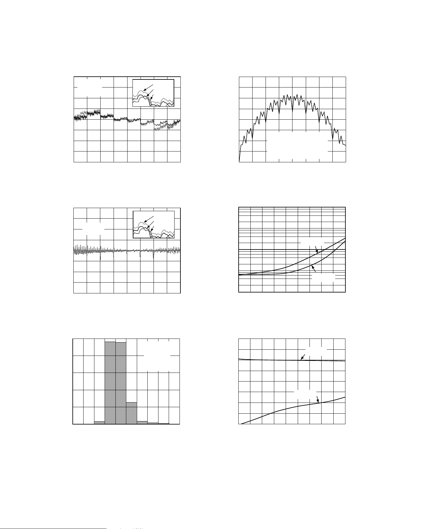
Figure 1. INL vs. Code
1
0.75
VDD = +5V
= +5V
V
0.5
0.25
INL – LSB
–0.25
–0.5
–0.75
REFH
= 0V
V
REFL
0
–1
0 25632 64 96 128 160 192 224
CODE – Decimal
TA = +85°C
= +25°C
T
A
= –40°C
T
A
TA = +85°C
= +25°C
T
A
= –40°C
T
A
160
140
120
100
80
CURRENT – µA
60
REF
I
40
20
0
0 25632 64 96 128 160 192 224
V
= +5V
DD
V
= +2V
REFH
V
= 0V
REFL
ONE DAC CHANGING WITH CODE,
OTHER DACs SET TO 00H
= +25°C
T
A
CODE – Decimal
Figure 4. Input Reference Current vs. Code
10k
1k
VDD = +5.5V
= +5.5V
V
100
10
SHUTDOWN CURRENT – nA
0
–35 255–15–55 65 1251058545
TEMPERATURE – °C
REF
VDD = +2.7V
V
REF
= +2.7V
Figure 2. Differential Nonlinearity Error vs. Code
1600
1280
960
640
FREQUENCY
320
0
0 0.2 0.4 0.6 0.8 1.0
ABSOLUTE VALUE TOTAL UNADJUSTED ERROR – LSB
VDD = +4.5V
= +4.5V
V
REF
= 0V
V
REFL
= +25°C
T
A
SS = 3600 PCS
Figure 3. Total Unadjusted Error Histogram
–4–
Figure 5. Shutdown Current vs. Temperature
Figure 6. Supply Current vs. Temperature
REV. 0

AD8802/AD8804
10
0%
100
90
OUTPUT1: 7FH → 80
H
VDD = +5V
V
REF
= +5V
TIME – 1µs/DIV
OUT1
5mV/DIV
CS
5V/DIV
5mV 1µs
5V
100
10
1.0
0.1
0.01
SUPPLY CURRENT – mA
0.001
0.0001
0.50
21.51
INPUT VOLTAGE – Volts
VDD = +3V
2.5
TA = +25°C
ALL DIGITAL INPUTS
TIED TOGETHER
VDD = +5V
53 4.543.5
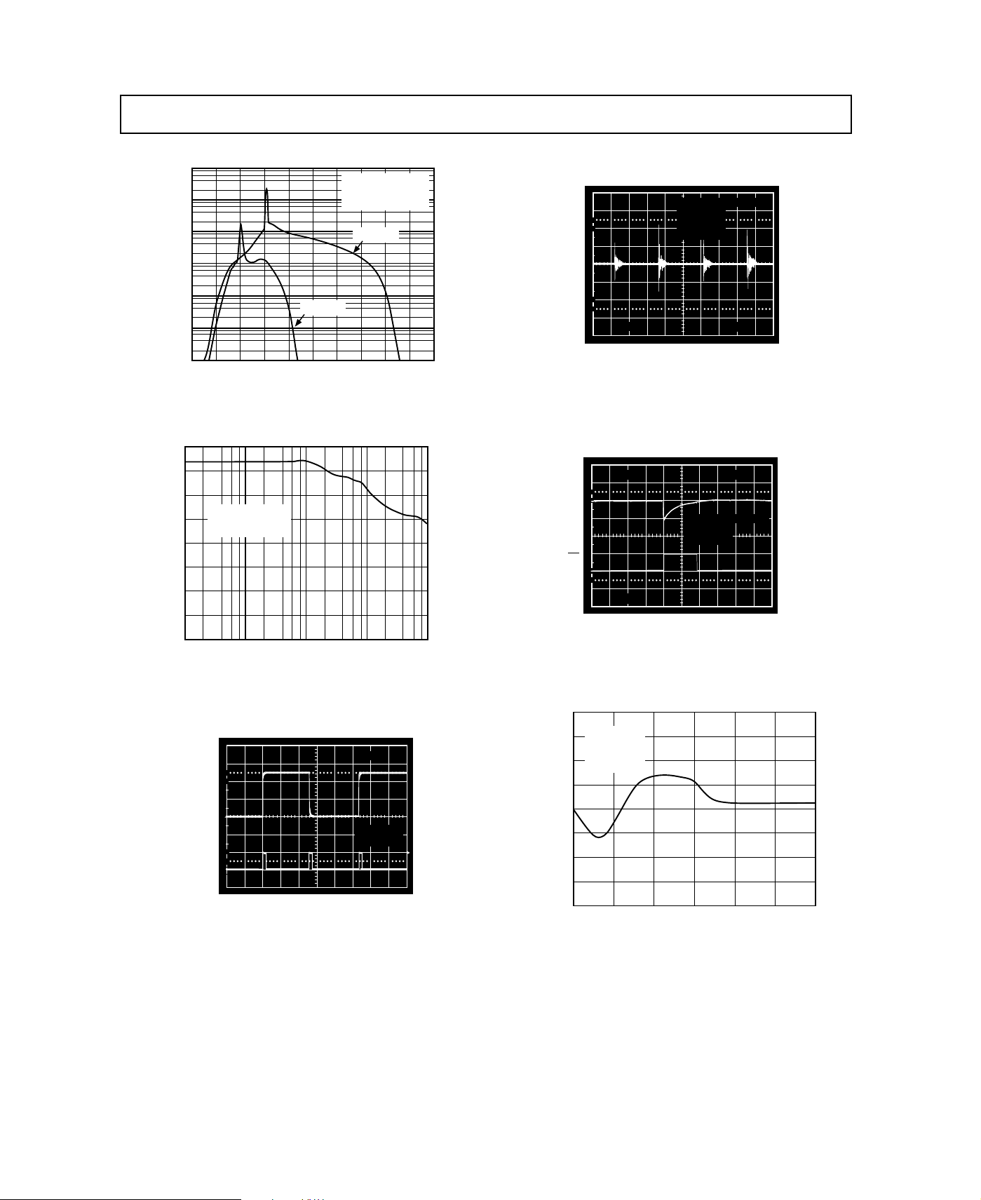
Figure 7. Supply Current vs. Logic Input Voltage
80
60
VDD = +5V
ALL OUTPUTS SET
TO MIDSCALE (80H)
40
PSRR – dB
100
90
10
OUTPUT2 – 10mV/DIV
0%
10mV
OUTPUT1: OOH → FF
V
= +5V
DD
V
= +5V
REF
f = 1MHz
TIME – 0.2µs/DIV
H
200ns
Figure 10. Adjacent Channel Clock Feedthrough
20
0
100 100k10k1k10
FREQUENCY – Hz
Figure 8. Power Supply Rejection vs. Frequency
OUT
2V
6V
100
90
4V
2V
0V
10
5V
0%
CS
0%
0V
5V
TIME – 5µs/DIV
5µs
VDD = +5V
V
= +5V
REF
Figure 9. Large-Signal Settling Time
Figure 11. Midscale Transition
0.01
VDD = +4.5V
V
= +4.5V
REF
SS = 176 PCS
0.005
V
= 0V
REFL
0
–0.005
CHANGE IN ZERO-SCALE ERROR – LSB
–0.01
0
200 400
HOURS OF OPERATION AT 150°C
600100 300 500
Figure 12. Zero-Scale Error Accelerated by Burn-In
REV. 0
–5–
 Loading...