Analog Devices AD7862AN-10, AD7862SQ-10, AD7862BR-3, AD7862BR-10, AD7862ARS-3 Datasheet
...
REV. 0
Information furnished by Analog Devices is believed to be accurate and
reliable. However, no responsibility is assumed by Analog Devices for its
use, nor for any infringements of patents or other rights of third parties
which may result from its use. No license is granted by implication or
otherwise under any patent or patent rights of Analog Devices.
a
AD7862
One Technology Way, P.O. Box 9106, Norwood, MA 02062-9106, U.S.A.
Tel: 617/329-4700 World Wide Web Site: http://www.analog.com
Fax: 617/326-8703 © Analog Devices, Inc., 1996
Simultaneous Sampling
Dual 250 kSPS 12-Bit ADC
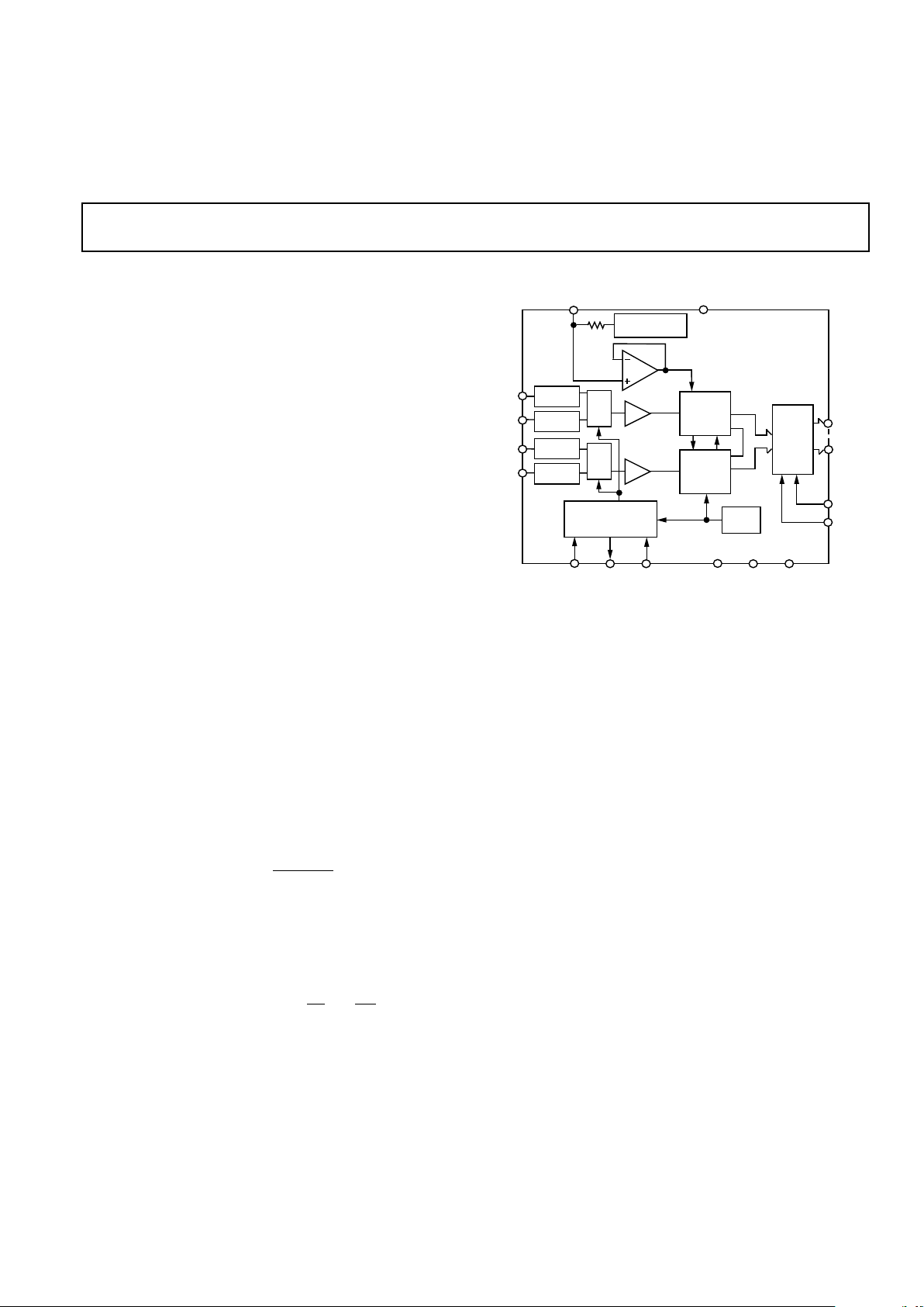
FUNCTIONAL BLOCK DIAGRAM
CLOCK
DGND
DB0
BUSY
RD
CS
CONVST
AD7862
CONVERSION
CONTROL LOGIC
V
A1
AGND
V
REF
+2.5V
REFERENCE
2kΩ
AGND
TRACK/
HOLD
V
DD
DB11
OUTPUT
LATCH
MUX
A0
12-BIT
ADC
12-BIT
ADC
TRACK/
HOLD
MUX
SIGNAL
SCALING
SIGNAL
SCALING
SIGNAL
SCALING
SIGNAL
SCALING
V
B1
V
A2
V
B2
FEATURES
Two Fast 12-Bit ADCs
Four Input Channels
Simultaneous Sampling & Conversion
4 ms Throughput Time
Single Supply Operation
Selection of Input Ranges:
610 V for AD7862-10
62.5 V for AD7862-3
0 V to 2.5 V for AD7862-2
High Speed Parallel Interface
Low Power, 60 mW typ
Power Saving Mode, 50 mW typ
Overvoltage Protection on Analog Inputs
14-Bit Pin Compatible Upgrade (AD7863)
APPLICATIONS
AC Motor Control
Uninterrupted Power Supplies
Data Acquisition Systems
Communications
GENERAL DESCRIPTION
The AD7862 is a high speed, low power, dual 12-bit A/D
converter that operates from a single +5 V supply. The part
contains two 4 µs successive approximation ADCs, two track/
hold amplifiers, an internal +2.5 V reference and a high speed
parallel interface. There are four analog inputs that are grouped
into two channels (A & B) selected by the A0 input. Each
channel has two inputs (V
A1
& V
A2
or V
B1
& VB2) that can be
sampled and converted simultaneously thus preserving the
relative phase information of the signals on both analog inputs.
The part accepts an analog input range of ± 10 V (AD7862-10),
±2.5 V (AD7862-3) and 0–2.5 V (AD7862-2). Overvoltage
protection on the analog inputs for the part allows the input
voltage to go to ±17 V, ±7 V or +7 V, respectively, without
causing damage.
A single conversion start signal (
CONVST) places both track/
holds into hold simultaneously and initiates conversion on both
inputs. The BUSY signal indicates the end of conversion, and
at this time the conversion results for both channels are available to be read. The first read after a conversion accesses the
result from V
A1
or VB1, while the second read accesses the result
from V
A2
or VB2, depending on whether the multiplexer select
A0 is low or high, respectively. Data is read from the part via a
12-bit parallel data bus with standard
CS and RD signals.
In addition to the traditional dc accuracy specifications such as
linearity, full-scale and offset errors, the part is also specified for
dynamic performance parameters including harmonic distortion
and signal-to-noise ratio.
The AD7862 is fabricated in Analog Devices’ Linear Compatible CMOS (LC
2
MOS) process, a mixed technology process
that combines precision bipolar circuits with low power CMOS
logic. It is available in 28-lead SSOP, SOIC and DIP.
PRODUCT HIGHLIGHTS
1. The AD7862 features two complete ADC functions allowing
simultaneous sampling and conversion of two channels. Each
ADC has a 2-channel input mux. The conversion result for
both channels is available 3.6 µs after initiating conversion.
2. The AD7862 operates from a single +5 V supply and
consumes 60 mW typ. The automatic power-down mode,
where the part goes into power down once conversion is
complete and “wakes up” before the next conversion cycle,
makes the AD7862 ideal for battery-powered or portable
applications.
3. The part offers a high speed parallel interface for easy con-
nection to microprocessors, microcontrollers and digital
signal processors.
4. The part is offered in three versions with different analog
input ranges. The AD7862-10 offers the standard industrial
input range of ±10 V; the AD7862-3 offers the common
signal processing input range of ±2.5 V; while the AD7862-2
can be used in unipolar 0 V – +2.5 V applications.
5. The part features very tight aperture delay matching between
the two input sample-and-hold amplifiers.

–2–
REV. 0
AD7862–SPECIFICATIONS
AB S
Parameter Version1Version Version Units Test Conditions/Comments
SAMPLE AND HOLD
–3 dB Small Signal Bandwidth 3 3 3 MHz typ
Aperture Delay 20 20 20 ns typ
Aperture Jitter 100 100 100 ps typ
Aperture Delay Matching 200 200 200 ps typ
DYNAMIC PERFORMANCE
2
fIN = 100.0 kHz, fS = 250 kSPS
Signal to (Noise+Distortion) Ratio
3
@ +25°C 70 71 70 dB min
T
MIN
to T
MAX
70 70 70 dB min
Total Harmonic Distortion
3
–78 –78 –78 dB max
Peak Harmonic or Spurious Noise
3
–85 –85 –85 dB typ
Intermodulation Distortion
3
fa = 49 kHz, fb = 50 kHz
2nd Order Terms –85 –85 –85 dB typ
3rd Order Terms –85 –85 –85 dB typ
Channel to Channel Isolation
3
–80 –80 –80 dB max fIN = 100 kHz Sine Wave
DC ACCURACY Any Channel
Resolution 12 12 12 Bits
Minimum Resolution for which
No Missing Codes are Guaranteed 12 12 12 Bits
Relative Accuracy
3
±1 ±1 ±1 LSB max Typically 0.4 LSB
Differential Nonlinearity
3
± 1 ±1 ±1 LSB max
Positive Gain Error
3
±4 ±3 ±4 LSB max
Positive Gain Error Match
3
4 3 4 LSB max
AD7862-10
Negative Gain Error
3
±4 ±3 ±4 LSB max
Bipolar Zero Error ±4 ±3 ±4 LSB max
Bipolar Zero Error Match 4 3 4 LSB max
AD7862-3
Negative Gain Error
3
±4 ±3 ±4 LSB max
Bipolar Zero Error ±4 ±3 ±4 LSB max
Bipolar Zero Error Match 4 3 4 LSB max
AD7862-2
Unipolar Offset Error +4 +3 +4 LSB max
Unipolar Offset Error Match 4 3.5 4 LSB max
ANALOG INPUTS
AD7862-10
Input Voltage Range ±10 ±10 ±10 Volts Input
Input Resistance 24 24 24 kΩ min
AD7862-3
Input Voltage Range ±2.5 ±2.5 ±2.5 Volts Input
Input Resistance 6 6 6 kΩ min
AD7862-2
Input Voltage Range +2.5 +2.5 +2.5 Volts Input
Input Current 500 500 500 nA max
REFERENCE INPUT/OUTPUT
REF IN Input Voltage Range 2.375/2.625 2.375/2.625 2.375/2.625 V min/V max 2.5 V ± 5%
REF IN Input Capacitance
4
10 10 10 pF max
REF OUT Output Voltage 2.5 2.5 2.5 V nom
REF OUT Error @ +25°C ±10 ±10 ±10 mV max
REF OUT Error T
MIN
to T
MAX
±25 ±25 ±25 mV max
REF OUT Temperature Coefficient 25 25 25 ppm/°C typ
REF OUT Output Impedance 2 2 2 kΩ nom
LOGIC INPUTS
Input High Voltage, V
INH
2.4 2.4 2.4 V min VDD = 5 V ± 5%
Input Low Voltage, V
INL
0.8 0.8 0.8 V max VDD = 5 V ± 5%
Input Current, I
IN
±10 ±10 ±10 µA max
Input Capacitance, C
IN
4
10 10 10 pF max
(VDD = +5 V 6 5%, AGND = DGND = 0 V, REF = Internal. All Specifications T
MIN
to T
MAX
unless otherwise noted.)

–3–
REV. 0
AD7862
AB S
Parameter Version1Version Version Units Test Conditions/Comments
LOGIC OUTPUTS
Output High Voltage, V
OH
4.0 4.0 4.0 V min I
SOURCE
= 200 µA
Output Low Voltage, V
OL
0.4 0.4 0.4 V max I
SINK
= 1.6 mA
DB11–DB0
Floating-State Leakage Current ±10 ±10 ±10 µA max
Floating-State Capacitance
4
10 10 10 pF max
Output Coding
AD7862-10, AD7862-3 Twos Complement
AD7863-2 Straight (Natural) Binary
CONVERSION RATE
Conversion Time 3.6 3.6 3.6 µs max For Both Channels
Track/Hold Acquisition Time
2, 3
0.3 0.3 0.3 µs max
POWER REQUIREMENTS
V
DD
+5 +5 +5 V nom ±5% for Specified Performance
I
DD
Normal Mode 15 15 15 mA max
Standby Mode 25 25 25 µA max Logic Inputs = 0 V or V
DD
Power Dissipation
Normal Mode 75 75 75 mW max Typically 60 mW
Standby Mode 125 125 125 µW max Typically 75 µW
NOTES
1
Temperature ranges are as follows: A, B Versions: –40°C to +85°C;
S Version: –55°C to +125°C.
2
Performance measured through full channel (multiplexer, SHA and ADC).
3
See Terminology.
ABSOLUTE MAXIMUM RATINGS*
(TA = +25°C unless otherwise noted)
VDD to AGND . . . . . . . . . . . . . . . . . . . . . . . . . –0.3 V to +7 V
V
DD
to DGND . . . . . . . . . . . . . . . . . . . . . . . . . –0.3 V to +7 V
AGND to DGND . . . . . . . . . . . . . . . . . . . . . . . . . . . . ±0.3 V
Analog Input Voltage to AGND
AD7862-10 . . . . . . . . . . . . . . . . . . . . . . . . . . . . . . . ±17 V
AD7862-3 . . . . . . . . . . . . . . . . . . . . . . . . . . . . . . . . . ±7V
AD7862-2 . . . . . . . . . . . . . . . . . . . . . . . . . . . . . . . . . +7 V
Reference Input Voltage to AGND . . . –0.3 V to V
DD
+ 0.3 V
Digital Input Voltage to DGND . . . . . –0.3 V to V
DD
+ 0.3 V
Digital Output Voltage to DGND . . . . –0.3 V to V
DD
+ 0.3 V
Operating Temperature Range
Commercial (A, B Version) . . . . . . . . . . . –40°C to +85°C
Extended (S Version) . . . . . . . . . . . . . . . . –55°C to +125°C
Storage Temperature Range . . . . . . . . . . . . –65°C to +150°C
Junction Temperature . . . . . . . . . . . . . . . . . . . . . . . . +150°C
Plastic DIP Package, Power Dissipation . . . . . . . . . . 670 mW
θ
JA
Thermal Impedance . . . . . . . . . . . . . . . . . . . . 116°C/W
Lead Temperature, (Soldering 10 sec) . . . . . . . . . . +260°C
Ceramic DIP Package, Power Dissipation . . . . . . . . . 670 mW
θ
JA
Thermal Impedance . . . . . . . . . . . . . . . . . . . . 116°C/W
Lead Temperature, (Soldering 10 sec) . . . . . . . . . . +260°C
SOIC Package, Power Dissipation . . . . . . . . . . . . . . . 450 mW
θ
JA
Thermal Impedance . . . . . . . . . . . . . . . . . . . . 110°C/W
Lead Temperature, Soldering
Vapor Phase (60 sec) . . . . . . . . . . . . . . . . . . . . . +215°C
Infrared (15 sec) . . . . . . . . . . . . . . . . . . . . . . . . . +220°C
SSOP Package, Power Dissipation . . . . . . . . . . . . . . . 450 mW
θ
JA
Thermal Impedance . . . . . . . . . . . . . . . . . . . . 110°C/W
Lead Temperature, Soldering
Vapor Phase (60 sec) . . . . . . . . . . . . . . . . . . . . . +215°C
Infrared (15 sec) . . . . . . . . . . . . . . . . . . . . . . . . . +220°C
*Stresses above those listed under “Absolute Maximum Ratings” may cause
permanent damage to the device. This is a stress rating only and functional
operation of the device at these or any other conditions above those listed in the
operational sections of this specification is not implied. Exposure to absolute
maximum rating conditions for extended periods may affect device reliability.
ORDERING GUIDE
Input Relative Temperature Package Package
Model Input Accuracy Range Description Option
AD7862AR-10 ±10 V ±1 LSB –40°C to +85°C 28-Bit Small Outline Package R-28
AD7862BR-10 ±10 V ±1 LSB –40°C to +85°C 28-Bit Small Outline Package R-28
AD7862ARS-10 ±10 V ±1 LSB –40°C to +85°C 28-Bit Shrink Small Outline Package RS-28
AD7862AN-10 ±10 V ±1 LSB –40°C to +85°C 28-Bit Plastic DIP N-28
AD7862SQ-10 ±10 V ±1 LSB –55°C to +125°C 28-Bit Cerdip Q-28
AD7862AR-3 ±2.5 V ±1 LSB –40°C to +85°C 28-Bit Small Outline Package R-28
AD7862BR-3 ±2.5 V ±1 LSB –40°C to +85°C 28-Bit Small Outline Package R-28
AD7862ARS-3 ± 2.5 V ±1 LSB –40°C to +85°C 28-Bit Shrink Small Outline Package RS-28
AD7862AN-3 ±2.5 V ±1 LSB –40°C to +85°C 28-Plastic DIP N-28
AD7862AR-2 0 V to 2.5 V ±1 LSB –40°C to +85°C 28-Bit Small Outline Package R-28
AD7862ARS-2 0 V to 2.5 V ±1 LSB –40°C to +85°C 28-Bit Shrink Small Outline Package RS-28
4
Sample tested @ +25°C to ensure compliance.
Specifications subject to change without notice.

AD7862
–4–
REV. 0
WARNING!
ESD SENSITIVE DEVICE
CAUTION
ESD (electrostatic discharge) sensitive device. Electrostatic charges as high as 4000 V readily
accumulate on the human body and test equipment and can discharge without detection.
Although the AD7862 features proprietary ESD protection circuitry, permanent damage may
occur on devices subjected to high energy electrostatic discharges. Therefore, proper ESD
precautions are recommended to avoid performance degradation or loss of functionality.
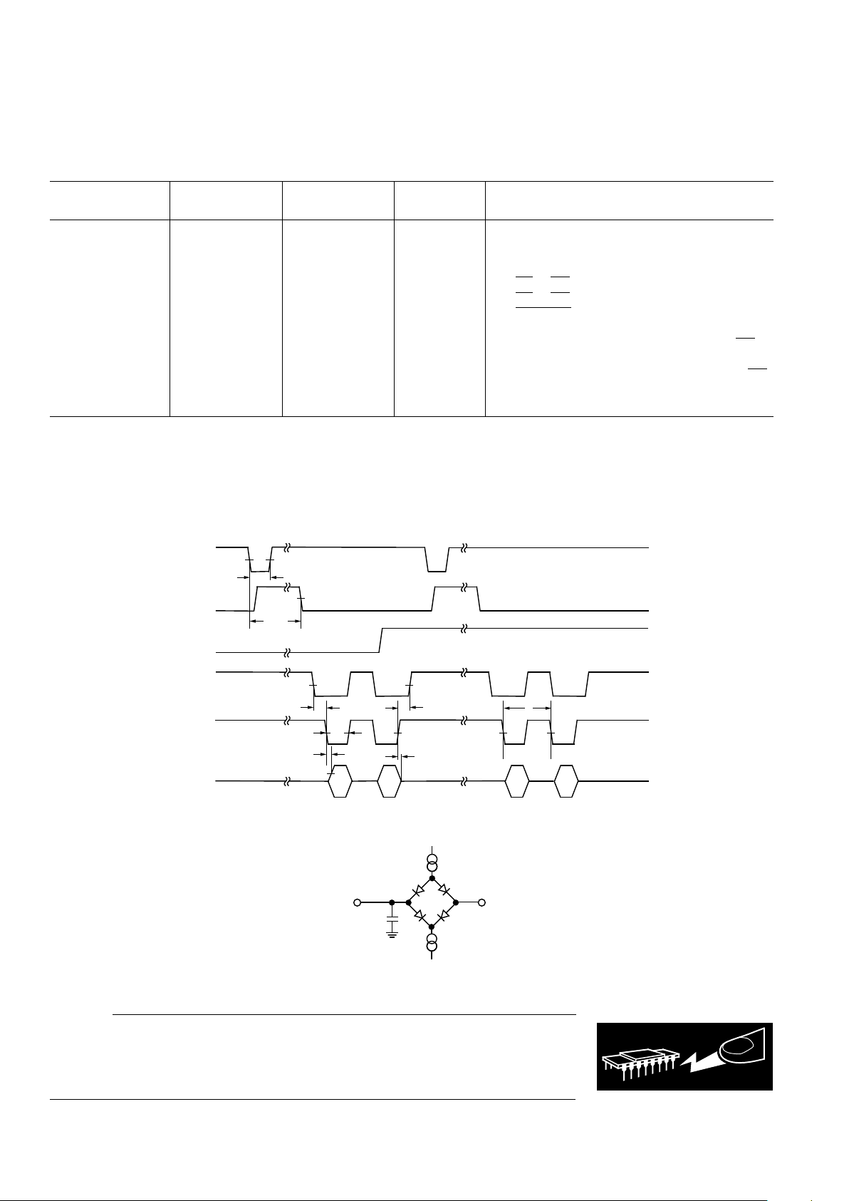
TIMING CHARACTERISTICS
1, 2
A, B S
Parameter Versions Version Units Test Conditions/Comments
t
CONV
3.6 3.6 µs max Conversion Time
t
ACQ
0.3 0.3 us max Acquisition Time
Parallel Interface
t
1
0 0 ns min CS to RD Setup Time
t
2
0 0 ns min CS to RD Hold Time
t
3
35 45 ns min CONVST Pulse Width
t
4
35 45 ns min Read Pulse Width
t
5
3
12 12 ns min Data Access Time After Falling Edge of RD
60 70 ns max
t
6
4
5 5 ns min Bus Relinquish Time After Rising Edge of RD
30 40 ns max
t
7
40 40 ns min Time Between Consecutive Reads
NOTES
1
Sample tested at +25°C to ensure compliance. All input signals are measured with tr = tf = 1 ns (10% to 90% of +5 V) and timed from a voltage level of +1.6 V.
2
See Figure 1.
3
Measured with the load circuit of Figure 2 and defined as the time required for an output to cross 0.8 V or 2.0 V.
4
These times are derived from the measured time taken by the data outputs to change 0.5 V when loaded with the circuit of Figure 2. The measured number is then
extrapolated back to remove the effects of charging or discharging the 50 pF capacitor. This means that the times quoted in the timing characteristics are the true bus
relinquish times of the part and as such are independent of external bus loading capacitances.
Specifications subject to change without notice.
(VDD = +5 V 6 5%, AGND = DGND = 0 V, REF = Internal. All Specifications T
MIN
to T
MAX
unless
otherwise noted.)
V
A1
V
A2
V
B1
V
B2
t
3
t
1
t
2
t
4
t
5
t
6
t
CONV
t
7
CONVST
BUSY
A0
CS
RD
DATA
......... .........
Figure 1. Timing Diagram
+1.6V
1.6mA
200µA
50pF
TO
OUTPUT
PIN
Figure 2. Load Circuit for Access Time and Bus Relinquish Time

AD7862
–5–
REV. 0
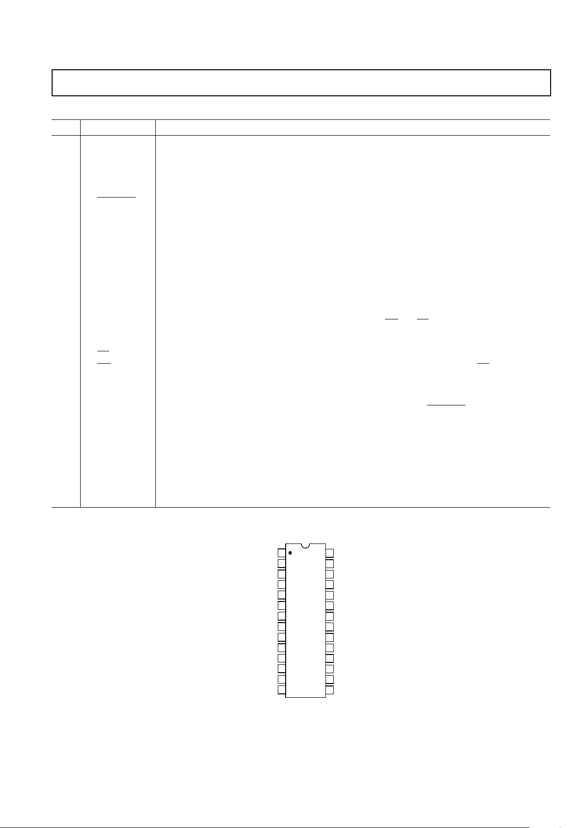
PIN FUNCTION DESCRIPTION
Pin Mnemonic Description
1 NC No Connect
2 DB11 Data Bit 11 (MSB). Three-state TTL output. Output coding is twos complement for the AD7862-
10 and AD7862-3. Output coding is straight (natural) binary for the AD7862-2.
3–6 DB10–DB7 Data Bit 10 to Data Bit 7. Three-state TTL outputs.
7 DGND Digital Ground. Ground reference for digital circuitry.
8
CONVST Convert Start Input. Logic Input. A high to low transition on this input puts both track/holds into
their hold mode and starts conversion on both channels.
9–15 DB6–DB0 Data Bit 6 to Data Bit 0. Three-state TTL outputs.
16 AGND Analog Ground. Ground reference for mux, track/hold, reference and DAC circuitry.
17 V
B2
Input Number 2 of Channel B. Analog Input voltage ranges of ±10 V (AD7862-10), ±2.5 V
(AD7862-3) and 0 V–2.5 V (AD7862-2).
18 V
A2
Input Number 2 of Channel A. Analog Input voltage ranges of ±10 V (AD7862-10), ± 2.5 V
(AD7862-3) and 0 V–2.5 V (AD7862-2).
19 VREF Reference Input/Output. This pin is connected to the internal reference through a series resistor and is
the output reference source for the analog-to-digital converter. The nominal reference voltage is 2.5 V,
and this appears at the pin.
20 A0 Multiplexer Select. This input is used in conjunction with
RD and CS low to enable the data outputs.
With A0 logic low, one read after a conversion will read the data from each of the ADCs in the sequence,
V
A1, VA2
, and a subsequent read, when A0 goes high, reads the data from VB1, VB2.
21
CS Chip Select Input. Active low logic input. The device is selected when this input is active.
22
RD Read Input. Active low logic input. This input is used in conjunction with A0 and CS low to enable
the data outputs. With A0 logic low, one read after a conversion will read the data from each of the
ADCs in the sequence, V
A1
, VA2, and a subsequent read, when A0 goes high, reads the data from V
B1,
VB2.
23 BUSY Busy Output. The busy output is triggered high by the falling edge of
CONVST and remains high
until conversion is completed.
24 VDD Analog and Digital Positive Supply Voltage, +5.0 V ± 5%.
25 V
A1
Input Number 1 of Channel A. Analog Input voltage ranges of ±10 V (AD7862-10), ± 2.5 V
(AD7862-3) and 0 V–2.5 V (AD7862-2).
26 V
B1
Input Number 1 of Channel B. Analog Input voltage ranges of ±10 V (AD7862-10), ±2.5 V
(AD7862-3) and 0 V–2.5 V (AD7862-2).
27 AGND Analog Ground. Ground reference for mux, track/hold, reference and DAC circuitry.
28 NC No Connect
PIN CONFIGURATION
14
13
12
11
17
16
15
20
19
18
10
9
8
1
2
3
4
7
6
5
TOP VIEW
(Not to Scale)
28
27
26
25
24
23
22
21
AD7862
NC = NO CONNECT
NC
V
A1
V
B1
AGND
NC
DB11
DB10
DB9
RD
BUSY
V
DD
DB8
DB7
DGND
CONVST
DB6
DB5
V
REF
A0
CS
DB4
DB3
DB2
DB1
V
A2
DB0
AGND
V
B2
 Loading...