Analog Devices AD7861 Datasheet

11-Bit Resolution
a
Simultaneous Sampling A/D Converter
FEATURES
11-Bit Resolution Analog-to-Digital Converter
Seven Single-Ended Analog Inputs
Four Input Channels Simultaneously Sampled
Expansion with 4 Multiplexed Inputs
Internal 2.5 V Reference
3.2 s Conversion Time per Channel
User Definable Channel Sequencing
Single Supply +5 V Operation
Double Buffered Register Outputs
6.25 MHz to 12.5 MHz Operating Clock Range
APPLICATIONS
Motor Control
3-Phase Power Measurement
Cellular Phones
Data Acquisition
GENERAL DESCRIPTION
The AD7861 is a multichannel simultaneous sampling A/D
Converter (ADC) configured for the acquisition of voltage
inputs in a motor control solution or three-phase power system.
The AD7861 combined with Analog Devices’ 16-bit fixedpoint digital signal processor (DSP) provides a low cost 16-bit
fixed-point microcontroller solution.
The input stage has been designed to accommodate the types of
signals frequently found in motor drives. The VIN1, VIN2, and
VIN3 channels are simultaneously sampled inputs suitable for
stator current acquisition. The AUX0–AUX3 channels are
multiplexed and are suitable for slower moving inputs such as
temperature and bus voltage of the diode rectifier output in a
motor control application.
AD7861
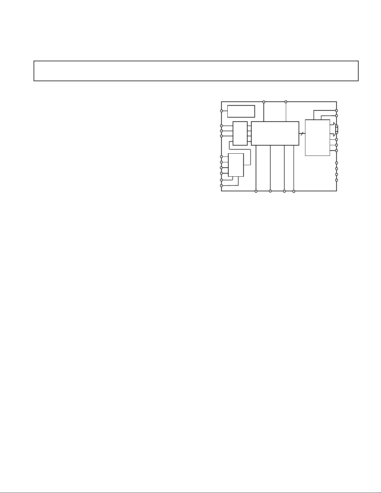
FUNCTIONAL BLOCK DIAGRAM
REF IN
REF OUT
VIN1
VIN2
VIN3
AUX0
AUX1
AUX2
AUX3
S0
S1
2.5V
REFERENCE
SHA
4-1
MUX
CONVST
PRODUCT HIGHLIGHTS
Simultaneous Sampling of Four Inputs
Four channel sample and hold amplifier (SHA) allows out of
phase input signals to be sampled simultaneously, preserving
the relative phase information. Sample-and-hold acquisition
time is 1.6 µs and conversion time per channel is 3.2 µs (using
a 12.5 MHz system clock).
Flexible Analog Channel Sequencing
AD7861 supports acquisition of 2, 3 or 4 channels per group.
Converted channel results are stored in registers and the data
can be read in any order. The sampling and conversion time
for two channels is 8 µs, three channels is 11.2 µs, and four
channels is 14.4 µs (using a 12.5 MHz system clock).
Single 5 V dc Operation
Low power, digital process.
11-BIT
ADC
RESET
BUSY
M0 M1
12
OUTPUT
REGISTERS
AD7861
A0
A1
D0
D11
RD
CS
CLKIN
SGND
AGND
DGND
V
DD
REV. B
Information furnished by Analog Devices is believed to be accurate and
reliable. However, no responsibility is assumed by Analog Devices for its
use, nor for any infringements of patents or other rights of third parties
which may result from its use. No license is granted by implication or
otherwise under any patent or patent rights of Analog Devices.
One Technology Way, P.O. Box 9106, Norwood, MA 02062-9106, U.S.A.
Tel: 781/329-4700 World Wide Web Site: http://www.analog.com
Fax: 781/326-8703 © Analog Devices, Inc., 2000

(VDD = 5 V ⴞ 5%; TA = –40ⴗC to +85ⴗC; REFIN = 2.5 V; Ext CLK @ 12.5 MHz, unless
AD7861–SPECIFICATIONS
otherwise noted)
Parameter AD7861AP Units Conditions/Comments
DC ACCURACY
Resolution 11 Bits Twos Complement Data Format
Relative Accuracy ± 2 LSB max Integral Nonlinearity
Differential Nonlinearity ± 2.5 LSB max
Bias Offset Error ± 9 LSB max Any Channel
Bias Offset Error Match 4 LSB max Between Channels
Full-Scale Error ± 13 LSB max Any Channel
Full-Scale Error Match 4 LSB max Between Channels
DYNAMIC PERFORMANCE
Signal-to-Noise Ratio (SNR) 60 dB min f
Total Harmonic Distortion (THD) –60 dB max f
Peak Harmonic or Spurious Noise –60 dB max f
= 1 kHz Sine Wave, f
IN
= 1 kHz Sine Wave, f
IN
= 1 kHz Sine Wave, f
IN
SAMPLE
SAMPLE
SAMPLE
= 75 kHz
= 75 kHz
= 75 kHz
Channel-to-Channel Isolation
M1 = 0 –58 dB max 1 kHz Sine Wave Applied to Unselected Channels
M1 = 1 –53 dB max 1 kHz Sine Wave Applied to Unselected Channels
REFERENCE
Input Voltage Range (REF IN) 2.5 V
Input Current 50 µA max
Onboard Reference Output (REF OUT) 2.5 V
Reference Tolerance ± 5%
Reference Drive Capability ± 100 µA max
SAMPLE-AND-HOLD
Acquisition Time 1.6 µs 20 CLK Cycles @ 12.5 MHz
Aperture Delay Time 200 ns max
Aperture Delay Time Match 20 ns max
Droop Rate 5 mV/ms max
LOGIC
Input High Voltage (V
Input Low Voltage (V
) 2 V min
IH
) 0.8 V max
IL
Input Leakage Current 1 µA max
Input Capacitance 20 pF typ
) 4.5 V min I
(V
OH
(V
) 0.4 V max I
OL
Current = 20 µA, VDD = 5 V
SOURCE
Current = 400 µA, VDD = 5 V
SINK
Three-State Leakage Current 1 µA max
CONVERSION RATE
Conversion Time/Channel 40 CLK Cycles
CONVST
Pulsewidth 2 CLK Cycles min
ANALOG INPUTS
Nominal Input Level 0–5 V VIN1, VIN2, VIN3, AUX0–AUX3
Input Current 100 µA
Input Capacitance 10 pF
SYSTEM CLOCK 6.25–12.5 MHz
POWER REQUIREMENTS
V
DD
I
DD
5V dc
10 mA max
– 2 –
REV. B
 Loading...