

3 V to 5 V Single Supply, 200 kSPS
a
8-Channel, 12-Bit Sampling ADCs
FEATURES
Specified for V
of 3 V to 5.5 V
DD
AD7859–200 kSPS; AD7859L–100 kSPS
System and Self-Calibration
Low Power
Normal Operation
AD7859: 15 mW (V
AD7859L: 5.5 mW (V
= 3 V)
DD
DD
= 3 V)
Using Automatic Power-Down After Conversion (25 mW)
AD7859: 1.3 mW (VDD = 3 V 10 kSPS)
AD7859L: 650 mW (V
= 3 V 10 kSPS)
DD
Flexible Parallel Interface:
16-Bit Parallel/8-Bit Parallel
44-Pin PQFP and PLCC Packages
APPLICATIONS
Battery-Powered Systems (Personal Digital Assistants,
Medical Instruments, Mobile Communications)
Pen Computers
Instrumentation and Control Systems
High Speed Modems
GENERAL DESCRIPTION
The AD7859/AD7859L are high speed, low power, 8-channel,
12-bit ADCs which operate from a single 3 V or 5 V power
supply, the AD7859 being optimized for speed and the
AD7859L for low power. The ADC contains self-calibration
and system calibration options to ensure accurate operation over
time and temperature and have a number of power-down
options for low power applications.
The AD7859 is capable of 200 kHz throughput rate while the
AD7859L is capable of 100 kHz throughput rate. The input
track-and-hold acquires a signal in 500 ns and features a pseudodifferential sampling scheme. The AD7859 and AD7859L input
voltage range is 0 to V
about V
/2 (bipolar) with both straight binary and 2s comple-
REF
(unipolar) and –V
REF
/2 to +V
REF
REF
/2
ment output coding respectively. Input signal range is to the
supply and the part is capable of converting full-power signals to
100 kHz.
CMOS construction ensures low power dissipation of typically
5.4 mW for normal operation and 3.6 µW in power-down mode.
The part is available in 44-pin, plastic quad flatpack package
(PQFP) and plastic lead chip carrier (PLCC).
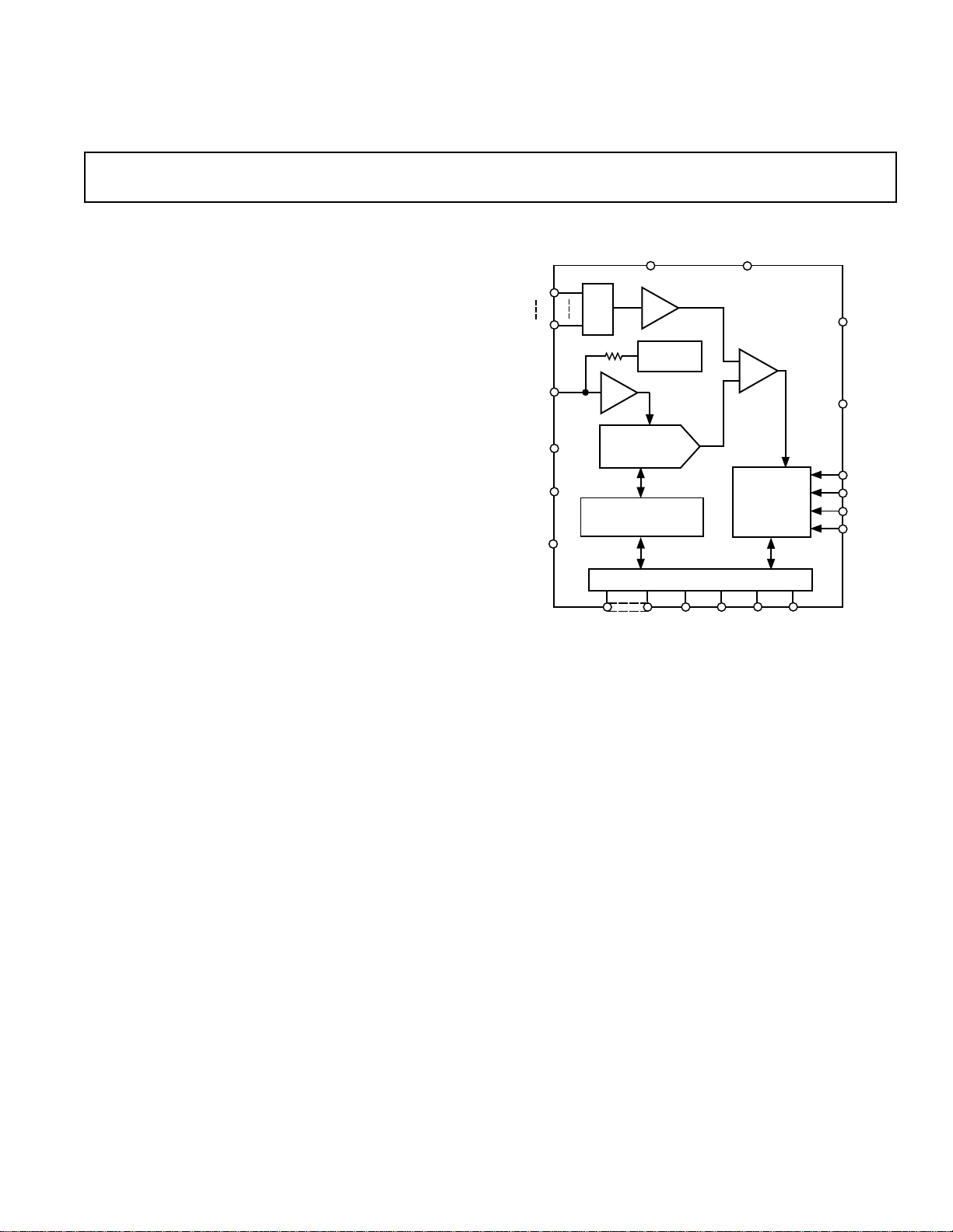
AD7859/AD7859L*
FUNCTIONAL BLOCK DIAGRAM
AV
DD
REF
REF
C
C
AIN1
AIN8
OUT
REF1
REF2
CAL
/
IN
I/P
MUX
CALIBRATION MEMORY
T/H
2.5V
REFERENCE
BUF
CHARGE
REDISTRIBUTION
DAC
AND
CONTROLLER
PARALLEL INTERFACE/CONTROL REGISTER
DB15 – DB0
RD
PRODUCT HIGHLIGHTS
1. Operation with either 3 V or 5 V power supplies.
2. Flexible power management options including automatic
power-down after conversion.
3. By using the power management options a superior power
performance at slower throughput rates can be achieved.
AD7859: 1 mW typ @ 10 kSPS
AD7859L: 1 mW typ @ 20 kSPS
4. Operates with reference voltages from 1.2 V to the supply.
5. Analog input ranges from 0 V to V
6. Self and system calibration.
7. Versatile parallel I/O port.
8. Lower power version AD7859L.
AGND
AD7859/AD7859L
COMP
SAR + ADC
CONTROL
WR
CS
DD
W/B
.
DV
DD
DGND
CLKIN
CONVST
BUSY
SLEEP
*Patent pending.
See page 28 for data sheet index.
REV. A
Information furnished by Analog Devices is believed to be accurate and
reliable. However, no responsibility is assumed by Analog Devices for its
use, nor for any infringements of patents or other rights of third parties
which may result from its use. No license is granted by implication or
otherwise under any patent or patent rights of Analog Devices.
© Analog Devices, Inc., 1996
One Technology Way, P.O. Box 9106, Norwood, MA 02062-9106, U.S.A.
Tel: 617/329-4700 Fax: 617/326-8703

1, 2
AD7859/AD7859L–SPECIFICATIONS
External Reference, f
(AD7859L); SLEEP = Logic High; TA = T
Parameter A Version1B Version1Units Test Conditions/Comments
DYNAMIC PERFORMANCE
Signal to Noise + Distortion Ratio370 71 dB min Typically SNR is 72 dB
(SNR) VIN = 10 kHz Sine Wave, f
Total Harmonic Distortion (THD) –78 –78 dB max VIN = 10 kHz Sine Wave, f
Peak Harmonic or Spurious Noise –78 –78 dB max VIN = 10 kHz Sine Wave, f
Intermodulation Distortion (IMD)
Second Order Terms –78 –78 dB typ fa = 9.983 kHz, fb = 10.05 kHz, f
Third Order Terms –78 –78 dB typ fa = 9.983 kHz, fb = 10.05 kHz, f
Channel-to-Channel Isolation –80 –80 dB typ VIN = 25 kHz
DC ACCURACY
Resolution 12 12 Bits
Integral Nonlinearity ±1 ± 0.5 LSB max 5 V Reference VDD = 5 V
Differential Nonlinearity ± 1 ±1 LSB max Guaranteed No Missed Codes to 12 Bits
Unipolar Offset Error ±5 ±5 LSB max
Unipolar Offset Error Match 2(3) 2 LSB max
Positive Full-Scale Error ±5 ±5 LSB max
Negative Full-Scale Error ± 2 ±2 LSB max
Full-Scale Error Match 1 1 LSB max
Bipolar Zero Error ±1 ±1 LSB typ
Bipolar Zero Error Match 2 2 LSB typ
= 4 MHz (for L Version: 1.8 MHz (08C to +708C) and 1 MHz (–408C to +858C)); f
CLKIN
to T
MIN
, unless otherwise noted.) Specifications in () apply to the AD7859L.
MAX
±2 ±2 LSB typ
±2 ±2 LSB typ
(AVDD = DVDD = +3.0 V to +5.5 V, REFIN/REF
= 200 kHz (AD7859) 100 kHz
SAMPLE
= 200 kHz
(for L Version: f
(for L Version: f
(for L Version: f
(for L Version: f
(for L Version: f
SAMPLE
SAMPLE
SAMPLE
SAMPLE
SAMPLE
SAMPLE
= 100 kHz @ f
= 200 kHz
SAMPLE
= 100 kHz @ f
= 200 kHz
SAMPLE
= 100 kHz @ f
= 100 kHz @ f
SAMPLE
= 100 kHz @ f
SAMPLE
= 2 MHz)
CLKIN
= 2 MHz)
CLKIN
= 2 MHz)
CLKIN
= 200 kHz
= 2 MHz)
CLKIN
= 200 kHz
= 2 MHz)
CLKIN
= 2.5 V
OUT
ANALOG INPUT
Input Voltage Ranges 0 to V
REF
0 to V
REF
Volts i.e., AIN(+) – AIN(–) = 0 to V
Biased Up But AIN(+) Cannot Go Below AIN(–)
±V
/2 ±V
REF
/2 Volts i.e., AIN(+) – AIN(–) = –V
REF
Should Be Biased to +V
Below AIN(–) But Cannot Go Below 0 V
Leakage Current ± 1 ± 1 µA max
Input Capacitance 20 20 pF typ
REFERENCE INPUT/OUTPUT
REFIN Input Voltage Range 2.3/V
DD
2.3/V
DD
V min/max Functional from 1.2 V
Input Impedance 150 150 kΩ typ
REF
Output Voltage 2.3/2.7 2.3/2.7 V min/max
OUT
REF
Tempco 20 20 ppm/°C typ
OUT
LOGIC INPUTS
Input High Voltage, V
INH
2.4 2.4 V min AV
2.1 2.1 V min AV
= DVDD = 4.5 V to 5.5 V
DD
= DVDD = 3.0 V to 3.6 V
DD
CAL Pin 3 3 V min AVDD = DVDD = 4.5 V to 5.5 V
2.4 2.4 V min AVDD = DVDD = 3.0 V to 3.6 V
Input Low Voltage, V
Input Current, I
IN
Input Capacitance, C
INL
IN
4
0.8 0.8 V max AV
0.6 0.6 V max AV
= DVDD = 4.5 V to 5.5 V
DD
= DVDD = 3.0 V to 3.6 V
DD
±10 ±10 µA max Typically 10 nA, V
10 10 pF max
IN
LOGIC OUTPUTS
Output High Voltage, V
OH
4 4 V min AVDD = DVDD = 4.5 V to 5.5 V
2.4 2.4 V min AVDD = DVDD = 3.0 V to 3.6 V
Output Low Voltage, V
OL
0.4 0.4 V max I
= 1.6 mA
SINK
Floating State Leakage Current ±10 ±10 µA max
Floating-State Output Capacitance410 10 pF max
Output Coding Straight (Natural) Binary Unipolar Input Range
2s Complement Bipolar Input Range
, AIN(–) Can Be
REF
/2 to +V
REF
/2 and AIN(+) Can Go
REF
= 0 V or V
DD
/2, AIN(–)
REF
–2–
REV. A
Parameter A Version1B Version1Units Test Conditions/Comments
AD7859/AD7859L
CONVERSION RATE t
CLKIN
× 18
Conversion Time 4.5 (10) 4.5 µs max (L Versions Only, 0°C to +70°C, 1.8 MHz CLKIN)
Track/Hold Acquisition Time 0.5 (1) 0.5 µs min (L Versions Only, –40°C to +85°C, 1.8 MHz CLKIN)
POWER REQUIREMENTS
AV
DD, DVDD
I
DD
Normal Mode
Sleep Mode
5
6
+3.0/+5.5 +3.0/+5.5 V min/max
5.5 (1.95) 5.5 mA max AV
5.5 (1.95) 5.5 mA max AV
= DVDD = 4.5 V to 5.5 V. Typically 4.5 mA
DD
= DVDD = 3.0 V to 3.6 V. Typically 4.0 mA
DD
With External Clock On 10 10 µA typ Full Power-Down. Power Management Bits in Control
Register Set as PMGT1 = 1, PMGT0 = 0.
400 400 µA typ Partial Power-Down. Power Management Bits in
Control Register Set as PMGT1 = 1, PMGT0 = 1.
With External Clock Off 5 5 µA max Typically 1 µA. Full Power-Down. Power Management
Bits in Control Register Set as PMGT1 = 1, PMGT0 = 0.
200 200 µA typ Partial Power-Down. Power Management Bits in
Control Register Set as PMGT1 = 1, PMGT0 = 1.
Normal Mode Power Dissipation 30 (10) 30 (10) mW max V
20 (6.5) 20 (6.5) mW max VDD = 3.6 V: Typically 15 mW (5.4); SLEEP = V
= 5.5 V: Typically 25 mW (8); SLEEP = V
DD
DD
DD
Sleep Mode Power Dissipation
With External Clock On 55 55 µW typ V
36 36 µW typ V
With External Clock Off 27.5 27.5 µW max V
= 5.5 V; SLEEP = 0 V
DD
= 3.6 V; SLEEP = 0 V
DD
= 5.5 V: Typically 5.5 µW; SLEEP = 0 V
DD
18 18 µW max VDD = 3.6 V: Typically 3.6 µW; SLEEP = 0 V
SYSTEM CALIBRATION
Offset Calibration Span
Gain Calibration Span
NOTES
1
Temperature range as follows: A, B Versions, –40°C to +85°C.
2
Specifications apply after calibration.
3
SNR calculation includes distortion and noise components.
4
Not production tested, guaranteed by characterization at initial product release.
5
All digital inputs @ DGND except for CONVST, SLEEP, CAL, and SYNC @ DVDD. No load on the digital outputs. Analog inputs @ AGND.
6
CLKIN @ DGND when external clock off. All digital inputs @ DGND except for CONVST, SLEEP, CAL, and SYNC @ DVDD. No load on the digital outputs.
Analog inputs @ AGND.
7
The offset and gain calibration spans are defined as the range of offset and gain errors that the AD7859/AD7859L can calibrate. Note also that these are voltage spans
and are not absolute voltages (i.e., the allowable system offset voltage presented at AIN(+) for the system offset error to be adjusted out will be AIN(–) ±0.05 × V
and the allowable system full-scale voltage applied between AIN(+) and AIN(–) for the system full-scale voltage error to be adjusted out will be V
This is explained in more detail in the calibration section of the data sheet.
7
7
+0.05 × V
+1.025 × V
/–0.05 × V
REF
/–0.975 × V
REF
V max/min Allowable Offset Voltage Span for Calibration
REF
V max/min Allowable Full-Scale Voltage Span for Calibration
REF
± 0.025 × V
REF
REF
REF
,
).
Specifications subject to change without notice.
REV. A
–3–
AD7859/AD7859L
(AV
= DVDD = +3.0 V to +5.5 V; f
DD
1
TIMING SPECIFICATIONS
Limit at T
MIN
, T
TA = T
MAX
MIN
to T
, unless otherwise noted)
MAX
(A, B Versions)
Parameter 5 V 3 V Units Description
2
f
CLKIN
500 500 kHz min Master Clock Frequency
4 4 MHz max
3
t
1
t
2
t
CONVERT
1.8 1.8 MHz max L Version
100 100 ns min CONVST Pulse Width
50 90 ns max CONVST to BUSY ↑ Propagation Delay
4.5 4.5 µs max Conversion Time = 18 t
10 10 µs max L Version 1.8 MHz CLKIN. Conversion Time = 18 t
t
3
t
4
t
5
t
6
t
7
4
t
8
5
t
9
15 15 ns min HBEN to RD Setup Time
5 5 ns min HBEN to RD Hold Time
0 0 ns min CS to RD to Setup Time
0 0 ns min CS to RD Hold Time
55 55 ns min RD Pulse Width
50 50 ns max Data Access Time After RD
5 5 ns min Bus Relinquish Time After RD
40 40 ns max Bus Relinquish Time After
t
10
t
11
t
12
t
13
t
14
t
15
t
16
t
17
4
t
18
t
19
6
t
CAL
6
t
CAL1
6
t
CAL2
NOTES
1
Sample tested at +25°C to ensure compliance. All input signals are specified with tr = tf = 5 ns (10% to 90% of VDD) and timed from a voltage level of 1.6 V.
2
Mark/Space ratio for the master clock input is 40/60 to 60/40.
3
The CONVST pulse width will here only apply for normal operation. When the part is in power-down mode, a different CONVST pulse width will apply (see PowerDown section).
4
Measured with the load circuit of Figure 1 and defined as the time required for the output to cross 0.8 V or 2.4 V.
5
t9 is derived form the measured time taken by the data outputs to change 0.5 V when loaded with the circuit of Figure 1. The measured number is then extrapolated
back to remove the effects of charging or discharging the 50 pF capacitor. This means that the time, t
time of the part and is independent of the bus loading.
6
The typical time specified for the calibration times is for a master clock of 4 MHz. For the L version the calibration times will be longer than those quoted here due to
the 1.8 MHz master clock.
Specifications subject to change without notice.
60 70 ns min Minimum Time Between Reads
0 0 ns min HBEN to WR Setup Time
5 5 ns max HBEN to WR Hold Time
0 0 ns min CS to WR Setup Time
0 0 ns max CS to WR Hold Time
55 70 ns min WR Pulse Width
10 10 ns min Data Setup Time Before WR
5 5 ns min Data Hold Time After WR
1/2 t
2.5 t
CLKIN
CLKIN
1/2 t
2.5 t
CLKIN
CLKIN
ns min New Data Valid Before Falling Edge of BUSY
ns max CS ↑ to BUSY ↑ in Calibration Sequence
31.25 31.25 ms typ Full Self-Calibration Time, Master Clock Dependent (125013
27.78 27.78 ms typ Internal DAC Plus System Full-Scale Cal Time, Master Clock
3.47 3.47 ms typ System Offset Calibration Time, Master Clock Dependent
= 4 MHz for AD7859 and 1.8 MHz for AD7859L;
CLKIN
CLKIN
RD
t
)
CLKIN
Dependent (111124 t
(13889 t
)
CLKIN
, quoted in the timing characteristics is the true bus relinquish
9
CLKIN
)
CLKIN
–4–
REV. A
AD7859/AD7859L
6
7
1
2
3
4
5
8
9
10
11
23
24
25
26
27
28
29
30
31
32
33
22
21
20
19
18
17
16
15
14
13
12
AD7859
TOP VIEW
(Not to Scale)
PIN NO. 1 IDENTIFIER
NC
W/B
REFIN/REF
OUT
AV
DD
C
REF1
AIN0
C
REF2
AGND
AIN1
AIN2
AIN3
DV
DD
DGND
DB5
DB6
DB7
DB8/HBEN
DB9
DB10
DB11
NC
DB4
CONVST
NC
DB14
CLKIN
BUSY
DB12
DB15
DB13
WR
RD
CS
NC
DB1
DB2
DB3
AIN4
AIN5
AIN6
AIN7
CAL
SLEEP
DB0
34
35
36
37
38
39
40
41
42
43
44
TO OUTPUT
PIN
1.6mA I
50pF
200µA I
OL
+2.1V
OH
Figure 1. Load Circuit for Digital Output Timing
Specifications
ORDERING GUIDE
Linearity Power
Error Dissipation Package
Model (LSB)
1
(mW) Option
2
AD7859AP ±1 15 P-44A
AD7859AS ±1 15 S-44
AD7859BS ±1/2 15 S-44
AD7859LAS
EVAL-AD7859CB
EVAL-CONTROL BOARD
NOTES
1
Linearity error refers to the integral linearity error.
2
P = PLCC; S = PQFP.
3
L signifies the low power version.
4
This can be used as a stand-alone evaluation board or in conjunction with the
EVAL-CONTROL BOARD for evaluation/demonstration purposes.
5
This board is a complete unit allowing a PC to control and communicate with
all Analog Devices, Inc. evaluation boards ending in the CB designators.
For more information on Analog Devices products and evaluation boards, visit
our World Wide Web home page at http://www.analog.com.
3
±1 5.5 S-44
4
5
ABSOLUTE MAXIMUM RATINGS
1
(TA = +25°C unless otherwise noted)
AVDD to AGND . . . . . . . . . . . . . . . . . . . . . . . . –0.3 V to +7 V
DV
to DGND . . . . . . . . . . . . . . . . . . . . . . . –0.3 V to +7 V
DD
AV
to DVDD . . . . . . . . . . . . . . . . . . . . . . . –0.3 V to +0.3 V
DD
Analog Input Voltage to AGND . . . . –0.3 V to AV
Digital Input Voltage to DGND . . . . –0.3 V to DV
Digital Output Voltage to DGND . . . –0.3 V to DV
REF
/REF
IN
Input Current to Any Pin Except Supplies
to AGND . . . . . . . . . –0.3 V to AVDD + 0.3 V
OUT
2
. . . . . . . . ±10 mA
+ 0.3 V
DD
+ 0.3 V
DD
+ 0.3 V
DD
Operating Temperature Range
Commercial (A, B Versions) . . . . . . . . . . . –40°C to +85°C
Storage Temperature Range . . . . . . . . . . . –65°C to +150°C
Junction Temperature . . . . . . . . . . . . . . . . . . . . . . . . . +150°C
PQFP Package, Power Dissipation . . . . . . . . . . . . . . 450 mW
θ
Thermal Impedance . . . . . . . . . . . . . . . . . . . . . 95°C/W
JA
Lead Temperature, Soldering
Vapor Phase (60 sec) . . . . . . . . . . . . . . . . . . . . . . +215°C
Infrared (15 sec) . . . . . . . . . . . . . . . . . . . . . . . . . . +220°C
PLCC Package, Power Dissipation . . . . . . . . . . . . . . 500 mW
θ
Thermal Impedance . . . . . . . . . . . . . . . . . . . . . . . 55°C/W
JA
Lead Temperature, Soldering
Vapor Phase (60 sec) . . . . . . . . . . . . . . . . . . . . . . +215°C
Infrared (15 sec) . . . . . . . . . . . . . . . . . . . . . . . . . . +220°C
ESD . . . . . . . . . . . . . . . . . . . . . . . . . . . . . . . . . . . . . >1500 kV
NOTES
1
Stresses above those listed under “Absolute Maximum Ratings” may cause
permanent damage to the device. This is a stress rating only and functional
operation of the device at these or any other conditions above those listed in the
operational sections of this specification is not implied. Exposure to absolute
maximum rating conditions for extended periods may affect device reliability.
2
Transient currents of up to 100 mA will not cause SCR latchup.
PINOUT FOR PLCC
WR
RD
CS
7
NC
8
W/B
REFIN/REF
9
OUT
AV
10
DD
11
12
13
14
15
16
17
18 19 20 21 22 23 24 25 26 27 28
AGND
C
REF1
C
REF2
AIN0
AIN1
AIN2
AIN3
AIN4
AIN5
AIN6
CONVST
BUSY
21443456
AD7859
TOP VIEW
(Not to Scale)
CAL
AIN7
CLKIN
SLEEP
DB15
DB0
DB14
DB1
42 41 4043
DB13
DB2
DB12
NC
NC
DB3
39
NC
DB11
38
37
DB10
36
DB9
35
DB8/HBEN
34
DGND
DV
33
32
DB7
31
DB6
30
DB5
29
DB4
DD
PINOUT FOR PQFP
REV. A
–5–

AD7859/AD7859L
TERMINOLOGY
Integral Nonlinearity
This is the maximum deviation from a straight line passing
through the endpoints of the ADC transfer function. The endpoints of the transfer function are zero scale, a point 1/2 LSB
below the first code transition, and full scale, a point 1/2 LSB
above the last code transition.
Differential Nonlinearity
This is the difference between the measured and the ideal 1 LSB
change between any two adjacent codes in the ADC.
Unipolar Offset Error
This is the deviation of the first code transition (00 . . . 000 to
00 . . . 001) from the ideal AIN(+) voltage (AIN(–) + 1/2 LSB)
when operating in the unipolar mode.
Positive Full-Scale Error
This applies to the unipolar and bipolar modes and is the deviation of the last code transition from the ideal AIN(+) voltage
(AIN(–) + Full Scale – 1.5 LSB) after the offset error has been
adjusted out.
Negative Full-Scale Error
This applies to the bipolar mode only and is the deviation of the
first code transition (10 . . . 000 to 10 . . . 001) from the ideal
AIN(+) voltage (AIN(–) – V
/2 + 0.5 LSB).
REF
Bipolar Zero Error
This is the deviation of the midscale transition (all 0s to all 1s)
from the ideal AIN(+) voltage (AIN(–) – 1/2 LSB).
Track/Hold Acquisition Time
The track/hold amplifier returns into track mode and the end of
conversion. Track/Hold acquisition time is the time required for
the output of the track/hold amplifier to reach its final value,
within ±1/2 LSB, after the end of conversion.
Signal to (Noise + Distortion) Ratio
This is the measured ratio of signal to (noise + distortion) at the
output of the A/D converter. The signal is the rms amplitude of
the fundamental. Noise is the sum of all nonfundamental signals up to half the sampling frequency (f
/2), excluding dc. The
S
ratio is dependent on the number of quantization levels in the
digitization process; the more levels, the smaller the quantization noise. The theoretical signal to (noise + distortion) ratio for
an ideal N-bit converter with a sine wave input is given by:
Signal to (Noise + Distortion) = (6.02 N +1.76)dB
Thus for a 12-bit converter, this is 74 dB.
Total Harmonic Distortion
Total harmonic distortion (THD) is the ratio of the rms sum of
harmonics to the fundamental. For the AD7859/AD7859L, it is
defined as:
2
2
2
2
2
+V
5
)
6
THD (dB) =20 log
(V
+V
+V
2
3
+V
4
V
1
where V1 is the rms amplitude of the fundamental and V2, V3,
V
, V5 and V6 are the rms amplitudes of the second through the
4
sixth harmonics.
Peak Harmonic or Spurious Noise
Peak harmonic or spurious noise is defined as the ratio of the
rms value of the next largest component in the ADC output
spectrum (up to f
/2 and excluding dc) to the rms value of the
S
fundamental. Normally, the value of this specification is determined by the largest harmonic in the spectrum, but for parts
where the harmonics are buried in the noise floor, it will be a
noise peak.
Intermodulation Distortion
With inputs consisting of sine waves at two frequencies, fa and
fb, any active device with nonlinearities will create distortion
products at sum and difference frequencies of mfa ± nfb where
m, n = 0, 1, 2, 3, etc. Intermodulation distortion terms are
those for which neither m nor n are equal to zero. For example,
the second order terms include (fa + fb) and (fa – fb), while the
third order terms include (2fa + fb), (2fa – fb), (fa + 2fb) and
(fa – 2fb).
Testing is performed using the CCIF standard where two input
frequencies near the top end of the input bandwidth are used. In
this case, the second order terms are usually distanced in frequency from the original sine waves while the third order terms
are usually at a frequency close to the input frequencies. As a
result, the second and third order terms are specified separately.
The calculation of the intermodulation distortion is as per the
THD specification where it is the ratio of the rms sum of the
individual distortion products to the rms amplitude of the sum
of the fundamentals expressed in dBs.
–6–
REV. A

AD7859/AD7859L
PIN FUNCTION DESCRIPTION
Mnemonic Description
CONVST Convert Start. Logic input. A low to high transition on this input puts the track/hold into its hold
mode and starts conversion. When this input is not used, it should be tied to DV
RD Read Input. Active low logic input. Used in conjunction with CS to read from internal registers.
WR Write Input. Active low logic input. Used in conjunction with CS to write to internal registers.
CS Chip Select Input. Active low logic input. The device is selected when this input is active.
/ Reference Input/Output. This pin is connected to the internal reference through a series resistor and is the
REF
IN
REF
OUT
reference source for the analog-to-digital converter. The nominal reference voltage is 2.5 V and this appears at the
pin. This pin can be overdriven by an external reference or can be taken as high as AV
AV
AV
DD
, then the C
DD
Analog Supply Voltage, +3.0 V to +5.5 V.
pin should also be tied to AVDD.
REF1
AGND Analog Ground. Ground reference for track/hold, reference and DAC.
DV
DD
Digital Supply Voltage, +3.0 V to +5.5 V.
DGND Digital Ground. Ground reference point for digital circuitry.
C
REF1
Reference Capacitor (0.1 µF multilayer ceramic). This external capacitor is used as a charge source for the inter-
nal DAC. The capacitor should be tied between the pin and AGND.
C
REF2
Reference Capacitor (0.01 µF ceramic disc). This external capacitor is used in conjunction with the on-chip refer-
ence. The capacitor should be tied between the pin and AGND.
AIN1–AIN8 Analog Inputs. Eight analog inputs which can be used as eight single ended inputs (referenced to AGND) or four
pseudo differential inputs. Channel configuration is selected by writing to the control register. None of the inputs
can go below AGND or above AV
B Word/Byte input. When this input is at a logic 1, data is transferred to and from the AD7859/AD7859L in 16-bit
W/
at any time. See Table III for channel selection.
DD
words on pins DB0 to DB15. When this pin is at a Logic 0, byte transfer mode is enabled. Data is transferred on
pins DB0 to DB7 and pin DB8/HBEN assumes its HBEN functionality.
DB0–DB7 Data Bits 0 to 7. Three state data I/O pins that are controlled by
CS, RD and WR. Data output is straight binary
(unipolar mode) or twos complement (bipolar mode).
DB8/HBEN Data Bit 8/High Byte Enable. When W/
trolled by
CS, RD and WR. When W/B is low, this pin acts as the High Byte Enable pin. When HBEN is low,
B is high, this pin acts as Data Bit 7, a three state data I/O pin that is con-
then the low byte of data being written to or read from the AD7859/AD7859L is on DB0 to DB7. When HBEN
is high, then the high byte of data being written to or read from the AD7859/AD7859L is on DB0 to DB7.
DB9–DB15 Data Bits 9 to 15. Three state data I/O pins that are controlled by
CS, RD and WR. Data output is straight bi-
nary (unipolar mode) or twos complement (bipolar mode).
CLKIN Master Clock Signal for the device (4 MHz for AD7859, 1.8 MHz for AD7859L). Sets the conversion and calibra-
tion times.
CAL Calibration Input. A logic 0 in this pin resets all logic. A rising edge on this pin initiates a calibration. This input
overrides all other internal operations.
BUSY Busy Output. The busy output is triggered high when a conversion or a calibration is initiated, and remains high
until the conversion or calibration is completed.
SLEEP Sleep Input. This pin is used in conjunction with the PGMT0 and PGMT1 bits in the control register to deter-
mine the power-down mode. Please see the “Power-Down Options” section for details.
NC No connect pins. These pins should be left unconnected.
DD
.
. When this pin is tied to
DD
REV. A
–7–
AD7859/AD7859L
TEST
REGISTER
CALIBRATION
REGISTERS
STATUS
REGISTER
GAIN (1)
OFFSET (1)
DAC (8)
GAIN (1)
OFFSET (1)
OFFSET (1) GAIN (1)
01 10 11
00 01 10 11
CALSLT1, CALSLT0
DECODE
ADC OUTPUT
DATA REGISTER
00
RDSLT1, RDSLT0
DECODE
AD7859/AD7859L ON-CHIP REGISTERS
The AD7859/AD7859L powers up with a set of default conditions. The only writing that is required is to select the channel configuration. Without performing any other write operations, the AD7859/AD7859L still retains the flexibility for performing a full powerdown and a full self-calibration.
Extra features and flexibility such as performing different power-down options, different types of calibrations, including system calibration, and software conversion start can be selected by writing to the part.
The AD7859/AD7859L contains a Control register, ADC output data register, Status register, Test register and 10 Cali-
bration registers. The control register is write-only, the ADC output data register and the status register are read-only, and the test
and calibration registers are both read/write registers. The test register is used for testing the part and should not be written to.
Addressing the On-Chip Registers
Writing
When writing to the AD7859/AD7859L, a 16-bit word of data must be transferred. The 16 bits of data is written as either a 16-bit
word, or as two 8-bit bytes, depending on the logic level at the W/
DB15, where DB0 is the LSB and DB15 is the MSB of the write. When W/
and data is transferred in two 8-bit bytes on pins DB0 to DB7, pin DB0 being the LSB of each transfer and pin DB7 being the MSB.
When writing to the AD7859/AD7859L in byte mode, the low byte must be written first followed by the high byte. The two MSBs
of the complete 16-bit word, ADDR1 and ADDR0, are decoded to determine which register is addressed, and the 14 LSBs are written to the addressed register. Table I shows the decoding of the address bits, while Figure 2 shows the overall write register hierarchy.
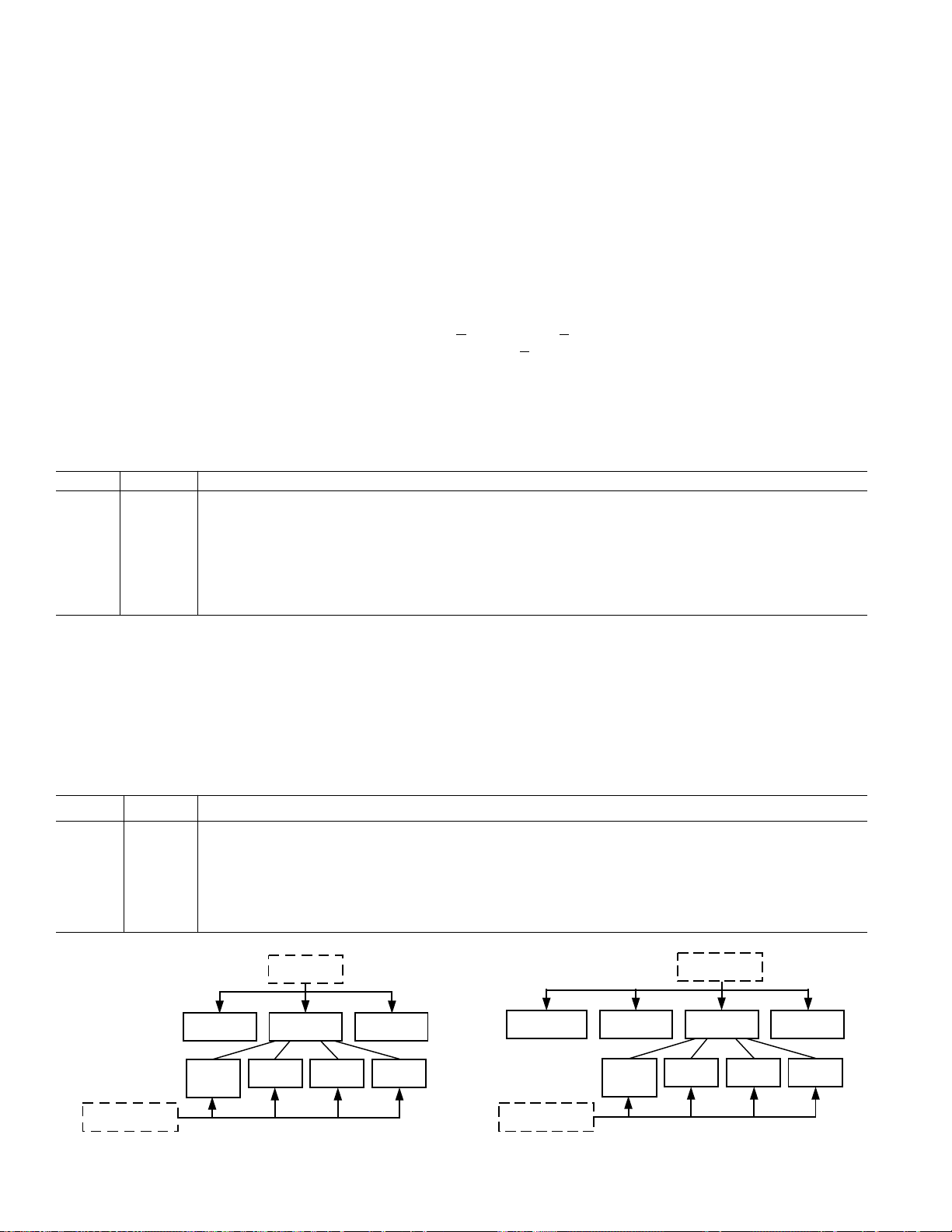
Table I. Write Register Addressing
ADDR1 ADDR0 Comment
0 0 This combination does not address any register.
0 1 This combination addresses the TEST REGISTER. The 14 LSBs of data are written to the test register.
1 0 This combination addresses the CALIBRATION REGISTERS. The 14 LSBs of data are written to the
selected calibration register.
1 1 This combination addresses the CONTROL REGISTER. The 14 LSBs of data are written to the control
register.
Reading
To read from the various registers the user must first write to Bits 6 and 7 in the Control Register, RDSLT0 and RDSLT1. These
bits are decoded to determine which register is addressed during a read operation. Table II shows the decoding of the read address
bits while Figure 3 shows the overall read register hierarchy. The power-up status of these bits is 00 so that the default read will be
from the ADC output data register. As with writing to the AD7859/AD7859L either word or byte mode can be used. When reading
from the calibration registers in byte mode, the low byte must be read first.
Once the read selection bits are set in the control register all subsequent read operations that follow are from the selected register until the read selection bits are changed in the control register.
Table II. Read Register Addressing
B pin. When W/B is high, the 16 bits are transferred on DB0 to
B is low, DB8/HBEN assumes its HBEN functionality
RDSLT1 RDSLT0 Comment
0 0 All successive read operations are from the ADC OUTPUT DATA REGISTER. This is the default power-
up setting. There is always four leading zeros when reading from the ADC output data register.
0 1 All successive read operations are from the TEST REGISTER.
1 0 All successive read operations are from the CALIBRATION REGISTERS.
1 1 All successive read operations are from the STATUS REGISTER.
ADDR1, ADDR0
DECODE
01 10 11
Figure 2. Write Register Hierarchy/Address Decoding
TEST
REGISTER
GAIN (1)
CALSLT1, CALSLT0
DECODE
OFFSET (1)
DAC (8)
00 01 10 11
CALIBRATION
REGISTERS
GAIN (1)
OFFSET (1)
OFFSET (1) GAIN (1)
CONTROL
REGISTER
Figure 3. Read Register Hierarchy/Address Decoding
–8–
REV. A
AD7859/AD7859L
CONTROL REGISTER
The arrangement of the control register is shown below. The control register is a write only register and contains 14 bits of data. The
control register is selected by putting two 1s in ADDR1 and ADDR0. The function of the bits in the control register is described
below. The power-up status of all bits is 0.
MSB
SGL/DIFF CHSLT2 CHSLT1 CHSLT0 PMGT1 PMGT0 RDSLT1
RDSLT0 AMODE CONVST CALMD CALSLT1 CALSLT0 STCAL
LSB
CONTROL REGISTER BIT FUNCTION DESCRIPTION
Bit Mnemonic Comment
13 SGL/
DIFF A 0 in this bit position configures the input channels for pseudo-differential mode. A 1 in this bit posi-
tion configures the input channels in single ended mode. Please see Table III for channel selection.
12 CHSLT2 These three bits are used to select the analog input on which the conversion is performed. The analog
11 CHSLT1 inputs can be configured as eight single-ended channels or four pseudo-differential channels. The
10 CHSLT0 default selection is AIN1 for the positive input and AIN2 for the negative input. Please see Table III for
channel selection information.
9 PMGT1 Power Management Bits. These two bits are used with the
SLEEP pin for putting the part into various
8 PMGT0 Power-Down modes (See Power-Down section for more details).
7 RDSLT1 Theses two bits determine which register is addressed for the read operations. Please see Table II.
6 RDSLT0
5 AMODE Analog Mode Bit. This bit has two different functions, depending on the status of the SGL/
When SGL/
this bit position selects the unipolar range, 0 to V
this bit position selects the bipolar range –V
+V
REF
swing from 0 V to +V
When SGL/
DIFF is 0, AMODE selects between unipolar and bipolar analog input ranges. A logic 0 in
(i.e., AIN(+) – AIN(–) = 0 to V
REF
/2 to +V
REF
/2). In this case AIN(–) needs to be tied to at least +V
.
REF
/2 (i.e., AIN(+) – AIN(–) = –V
REF
/2 to allow AIN(+) to have a full input
REF
DIFF is 1, AMODE selects the source for the AIN(–) channel of the sample and hold cir-
DIFF bit.
). A logic 1 in
REF
REF
/2 to
cuitry. If AMODE is a 0, AGND is selected. If AMODE is a 1, then AIN8 is selected. Please see
Table III for more information.
4 CONVST Conversion Start Bit. A logic 1 in this bit position starts a single conversion, and this bit is automatically
reset to 0 at the end of conversion. This bit may also be used in conjunction with system calibration (see
calibration section on page 21).
3 CALMD Calibration Mode Bit. A 0 here selects self-calibration and a 1 selects a system calibration (see Table IV).
2 CALSLT1 Calibration Selection Bits 1 and 0. These bits have two functions, depending on the STCAL bit.
1 CALSLT0 With the STCAL bit set to 1, the CALSLT1 and CALSLT0 bits, along with the CALMD bit, deter-
mine the type of calibration performed by the part (see Table IV).
With the STCAL bit set to 0, the CALSLT1 and CALSLT0 bits are decoded to address the calibration
register for read/write of calibration coefficients (see Table V for more details).
0 STCAL Start Calibration Bit. When STCAL is set to a 1, a calibration is performed, as determined by the
CALMD, CALSLT1 and CALSLT0 bits. Please see Table IV. When STCAL is set to a zero, no cali-
bration is performed.
REV. A
–9–

AD7859/AD7859L
Table IIIa. Channel Selection for AD7859/AD7859L
Differential Sampling (SGL/DIFF = 0)
AMODE CHSLT AIN(+)*AIN(–)* Bipolar or
2 1 0 Unipolar
0 0 0 0 AIN1 AIN2 Unipolar
0 0 0 1 AIN3 AIN4 Unipolar
0 0 1 0 AIN5 AIN6 Unipolar
0 0 1 1 AIN7 AIN8 Unipolar
0 1 x x x x Not Used
1 0 0 0 AIN1 AIN2 Bipolar
1 0 0 1 AIN3 AIN4 Bipolar
1 0 1 0 AIN5 AIN6 Bipolar
1 0 1 1 AIN7 AIN8 Bipolar
1 1 x x x x Not Used
*AIN(+) refers to the positive input seen by the AD7859/AD7859L sample-and-
hold circuitry.
AIN(–) refers to the negative input seen by the AD7859/AD7859L sample-and-
hold circuitry.
Table IIIb. Channel Selection for AD7859/AD7859L
Single-Ended Sampling (SGL/DIFF = 1)
AMODE CHSLT AIN(+)*AIN(–)* Bipolar or
2 1 0 Unipolar
0 0 0 0 AIN1 AGND Unipolar
0 0 0 1 AIN3 AGND Unipolar
0 0 1 0 AIN5 AGND Unipolar
0 0 1 1 AIN7 AGND Unipolar
0 1 0 0 AIN2 AGND Unipolar
0 1 0 1 AIN4 AGND Unipolar
0 1 1 0 AIN6 AGND Unipolar
0 1 1 1 AIN8 AGND Unipolar
1 0 0 0 AIN1 AIN8 Unipolar
1 0 0 1 AIN3 AIN8 Unipolar
1 0 1 0 AIN5 AIN8 Unipolar
1 0 1 1 AIN7 AIN8 Unipolar
1 1 0 0 AIN2 AIN8 Unipolar
1 1 0 1 AIN4 AIN8 Unipolar
1 1 1 0 AIN6 AIN8 Unipolar
1 1 1 1 AIN8 AIN8 Unipolar
Table IV. Calibration Selection
CALMD CALSLT1 CALSLT0 Calibration Type
00 0 A full internal calibration is initiated. First the internal DAC is calibrated, then the
internal gain error and finally the internal offset error are removed. This is the default setting.
0 0 1 First the internal gain error is removed, then the internal offset error is removed.
0 1 0 The internal offset error only is calibrated out.
0 1 1 The internal gain error only is calibrated out.
10 0 A full system calibration is initiated. First the internal DAC is calibrated, followed by the
system gain error calibration, and finally the system offset error calibration.
1 0 1 First the system gain error is calibrated out, followed by the system offset error.
1 1 0 The system offset error only is removed.
1 1 1 The system gain error only is removed.
–10–
REV. A

AD7859/AD7859L
STATUS REGISTER
The arrangement of the status register is shown below. The status register is a read-only register and contains 16 bits of data. The
status register is selected by first writing to the control register and putting two 1s in RDSLT1 and RDSLT0. The function of the
bits in the status register are described below. The power-up status of all bits is 0.
START
WRITE TO CONTROL REGISTER
SETTING RDSLT0 = RDSLT1 = 1
READ STATUS REGISTER
Figure 4. Flowchart for Reading the Status Register
MSB
ZERO ZERO SGL/DIFF CHSLT2 CHSLT1 CHSLT0 PMGT1 PMGT0
ONE ONE AMODE BUSY CALMD CALSLT1 CALSLT0 STCAL
LSB
STATUS REGISTER BIT FUNCTION DESCRIPTION
Bit Mnemonic Comment
15 ZERO These two bits are always 0.
14 ZERO
13 SGL/
12 CHSLT2 Channel Selection Bits. These bits, in conjunction with the SGL/
DIFF Single/Differential Bit.
DIFF bit, determine which channel has
11 CHSLT1 been selected for conversion. Please refer to Table IIIa and Table IIIb.
10 CHSLT0
9 PMGT1 Power Management Bits. These bits along with the
SLEEP pin indicate if the part is in a power-down
8 PMGT0 mode or not. See Table VI in Power-Down Section for description.
7 ONE Both these bits are always 1.
6 ONE
5 AMODE Analog Mode Bit. This bit is used along with SGL/DIFF and CHSLT2 – CHSLT0 to determine the
AIN(+) and AIN(–) inputs to the track and hold circuitry and the analog conversion mode (unipolar or bipolar). Please see Table III for details.
4 BUSY Conversion/Calibration BUSY Bit. When this bit is a 1, there is a conversion or a calibration in progress.
When this bit is a zero, there is no conversion or calibration in progress.
3 CALMD Calibration Mode Bit. A 0 in this bit indicates a self-calibration is selected, and a 1 in this bit indicates a
system calibration is selected (see Table IV).
2 CALSLT1 Calibration Selection Bits. The CALSLT1 and CALSLT0 bits indicate which of the calibration
1 CALSLT0 registers are addressed for reading and writing (see section on the Calibration Registers for more details).
0 STCAL Start Calibration Bit. The STCAL bit is a 1 if a calibration is in progress and a 0 if there is no calibration in
progress.
REV. A
–11–

AD7859/AD7859L
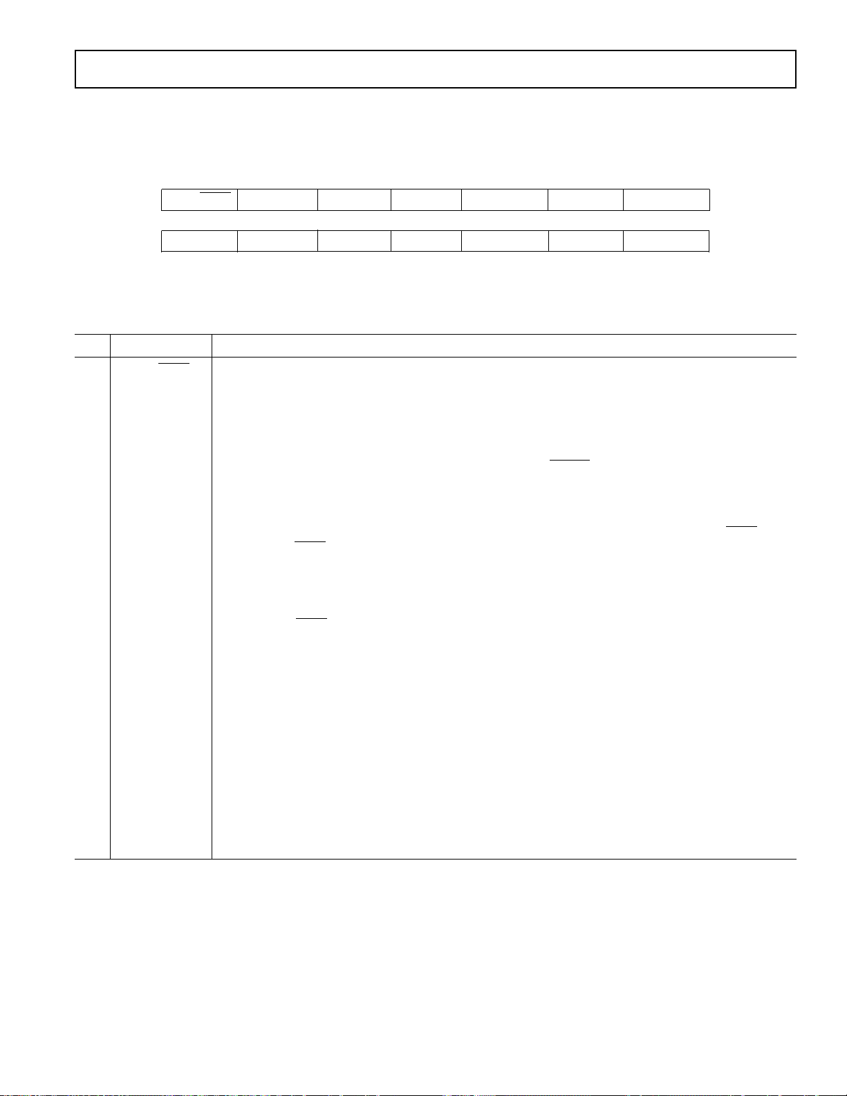
START
WRITE TO CAL REGISTER
(ADDR1 = 1, ADDR0 = 0)
FINISHED
LAST
REGISTER
WRITE
OPERATION
OR
ABORT
?
YES
NO
CAL REGISTER POINTER IS
AUTOMATICALLY RESET
WRITE TO CONTROL REGISTER SETTING STCAL = 0
AND CALSLT1, CALSLT0 = 00, 01, 10, 11
CAL REGISTER POINTER IS
AUTOMATICALLY INCREMENTED
CALIBRATION REGISTERS
The AD7859/AD7859L has 10 calibration registers in all, 8 for the DAC, 1 for offset and 1 for gain. Data can be written to or read
from all 10 calibration registers. In self and system calibration, the part automatically modifies the calibration registers; only if the
user needs to modify the calibration registers should an attempt be made to read from and write to the calibration registers.
Addressing the Calibration Registers
The calibration selection bits in the control register CALSLT1 and CALSLT0 determine which of the calibration registers are addressed (See Table V). The addressing applies to both the read and write operations for the calibration registers. The user should not
attempt to read from and write to the calibration registers at the same time.
Table V. Calibration Register Addressing
CALSLT1 CALSLT0 Comment
0 0 This combination addresses the Gain (1), Offset (1) and DAC Registers (8). Ten registers in total.
0 1 This combination addresses the Gain (1) and Offset (1) Registers. Two registers in total.
1 0 This combination addresses the Offset Register. One register in total.
1 1 This combination addresses the Gain Register. One register in total.
Writing to/Reading from the Calibration Registers
When writing to the calibration registers a write to the control
register is required to set the CALSLT0 and CALSLT1 bits.
When reading from the calibration registers a write to the control register is required to set the CALSLT0 and CALSLT1 bits
and also to set the RDSLT1 and RDSLT0 bits to 10 (this addresses the calibration registers for reading). The calibration
register pointer is reset on writing to the control register setting
the CALSLT1 and CALSLT0 bits, or upon completion of all
the calibration register write/read operations. When reset it
points to the first calibration register in the selected write/read
sequence. The calibration register pointer points to the gain
calibration register upon reset in all but one case, this case being
where the offset calibration register is selected on its own
(CALSLT1 = 1, CALSLT0 = 0). Where more than one calibration register is being accessed, the calibration register pointer
is automatically incremented after each full calibration register
write/read operation. The calibration register address pointer is
incremented after the high byte read or write operation in byte
mode. Therefore when reading (in byte mode) from the calibration registers, the low byte must always be read first, i.e., HBEN
= logic zero. The order in which the 10 calibration registers are
arranged is shown in Figure 5. Read/Write operations may be
aborted at any time before all the calibration registers have been
accessed, and the next control register write operation resets the
calibration register pointer. The flowchart in Figure 6 shows the
sequence for writing to the calibration registers. Figure 7 shows
the sequence for reading from the calibration registers.
CAL REGISTER
ADDRESS POINTER
CALIBRATION REGISTERS
GAIN REGISTER
OFFSET REGISTER
DAC 1st MSB REGISTER
When reading from the calibration registers there is always two
leading zeros for each of the registers.
Figure 6. Flowchart for Writing to the Calibration Registers
(1)
(2)
(3)
CALIBRATION REGISTER ADDRESS POINTER POSITION IS
DETERMINED BY THE NUMBER OF CALIBRATION REGISTERS
ADDRESSED AND THE NUMBER OF READ/WRITE OPERATIONS.
Figure 5. Calibration Register Arrangement
DAC 8th MSB REGISTER
(10)
–12–
REV. A
AD7859/AD7859L
START
WRITE TO CONTROL REGISTER SETTING STCAL = 0, RDSLT1 = 1,
RDSLT0 = 0, AND CALSLT1, CALSLT0 = 00, 01, 10, 11
CAL REGISTER POINTER IS
AUTOMATICALLY RESET
READ CAL REGISTER
CAL REGISTER POINTER IS
AUTOMATICALLY INCREMENTED
LAST
REGISTER
WRITE
OPERATION
OR
ABORT
?
FINISHED
NO
YES
Figure 7. Flowchart for Reading from the Calibration
Registers
Adjusting the Offset Calibration Register
The offset calibration register contains 16 bits. The two MSBs
are zero and the 14 LSBs contain offset data. By changing the
contents of the offset register, different amounts of offset on the
analog input signal can be compensated for. Decreasing the
number in the offset calibration register compensates for negative offset on the analog input signal, and increasing the number
in the offset calibration register compensates for positive offset
on the analog input signal. The default value of the offset calibration register is 0010 0000 0000 0000 approximately. This is
not the exact value, but the value in the offset register should be
close to this value. Each of the 14 data bits in the offset register
is binary weighted; the MSB has a weighting of 5% of the refer-
ence voltage, the MSB-1 has a weighting of 2.5%, the MSB-2
has a weighting of 1.25%, and so on down to the LSB which has
a weighting of 0.0006%. This gives a resolution of ±0.0006% of
V
approximately. The resolution can also be expressed as
REF
±(0.05 × V
13
)/2
volts. This equals ±0.015 mV, with a 2.5 V
REF
reference. The maximum offset that can be compensated for is
±5% of the reference voltage, which equates to ±125 mV with a
2.5 V reference and ±250 mV with a 5 V reference.
Q. If a +20 mV offset is present in the analog input signal and the
reference voltage is 2.5 V, what code needs to be written to the
offset register to compensate for the offset ?
A. 2.5 V reference implies that the resolution in the offset reg-
ister is 5% × 2.5 V/2
13
= 0.015 mV. +20 mV/0.015 mV =
1310.72; rounding to the nearest number gives 1311. In
binary terms this is 00 0101 0001 1111, therefore increase
the offset register by 00 0101 0001 1111.
This method of compensating for offset in the analog input signal allows for fine tuning the offset compensation. If the offset
on the analog input signal is known, there is no need to apply
the offset voltage to the analog input pins and do a system calibration. The offset compensation can take place in software.
Adjusting the Gain Calibration Register
The gain calibration register contains 16 bits. The two MSBs
are zero and the 14 LSBs contain gain data. As in the offset calibrating register the data bits in the gain calibration register are
binary weighted, with the MSB having a weighting of 2.5% of
the reference voltage. The gain register value is effectively multiplied by the analog input to scale the conversion result over the
full range. Increasing the gain register compensates for a
smaller analog input range and decreasing the gain register compensates for a larger input range. The maximum analog input
range that the gain register can compensate for is 1.025 times
the reference voltage, and the minimum input range is 0.975
times the reference voltage.
REV. A
–13–

AD7859/AD7859L
CIRCUIT INFORMATION
The AD7859/AD7859L is a fast, 8-channel, 12-bit, single supply A/D converter. The part requires an external 4 MHz/1.8
MHz master clock (CLKIN), two C
capacitors, a CONVST
REF
signal to start conversion and power supply decoupling capacitors. The part provides the user with track/hold, on-chip reference, calibration features, A/D converter and parallel interface
logic functions on a single chip. The A/D converter section of
the AD7859/AD7859L consists of a conventional successive-approximation converter based around a capacitor DAC. The
AD7859/AD7859L accepts an analog input range of 0 to +V
V
can be tied to VDD. The reference input to the part con-
REF
REF.
nected via a 150 kΩ resistor to the internal 2.5 V reference and
to the on-chip buffer.
A major advantage of the AD7859/AD7859L is that a conversion can be initiated in software, as well as by applying a signal
to the
CONVST pin. The part is available in a 44-pin PLCC or a
44-pin PQFP package, and this offers the user considerable
spacing saving advantages over alternative solutions. The
AD7859L version typically consumes only 5.5 mW making it
ideal for battery-powered applications.
CONVERTER DETAILS
The master clock for the part is applied to the CLKIN pin.
Conversion is initiated on the AD7859/AD7859L by pulsing the
CONVST input or by writing to the control register and setting
the CONVST bit to 1. On the rising edge of
CONVST (or at
the end of the control register write operation), the on-chip
track/hold goes from track to hold mode. The falling edge of the
CLKIN signal which follows the rising edge of
tiates the conversion, provided the rising edge of
CONVST ini-
CONVST (or
WR when converting via the control register) occurs typically at
least 10 ns before this CLKIN edge. The conversion takes 16.5
CLKIN periods from this CLKIN falling edge. If the 10 ns setup time is not met, the conversion takes 17.5 CLKIN periods.
The time required by the AD7859/AD7859L to acquire a signal
depends upon the source resistance connected to the AIN(+) input. Please refer to the acquisition time section for more details.
When a conversion is completed, the BUSY output goes low,
and the result of the conversion can be read by accessing the
data through the data bus. To obtain optimum performance
from the part, read or write operations should not occur during
the conversion or less than 200 ns prior to the next
CONVST
rising edge. Reading/writing during conversion typically degrades the Signal-to-(Noise + Distortion) by less than 0.5 dBs.
The AD7859 can operate at throughput rates of over 200 kSPS
(up to 100 kSPS for the AD7859L).
With the AD7859L, 100 kSPS throughput can be obtained as
follows: the CLKIN and
CONVST signals are arranged to give
a conversion time of 16.5 CLKIN periods as described above
and 1.5 CLKIN periods are allowed for the acquisition time.
With a 1.8 MHz clock, this gives a full cycle time of 10 µs,
which equates to a throughput rate of 100 kSPS.
When using the software conversion start for maximum
throughput, the user must ensure the control register write operation extends beyond the falling edge of BUSY. The falling
edge of BUSY resets the
CONVST bit to 0 and allows it to be
reprogrammed to 1 to start the next conversion.
TYPICAL CONNECTION DIAGRAM
Figure 8 shows a typical connection diagram for the AD7859/
AD7859L. The AGND and the DGND pins are connected
together at the device for good noise suppression. The first
CONVST applied after power-up starts a self-calibration
sequence. This is explained in the calibration section of this data
sheet. Note that after power is applied to AV
the
CONVST signal is applied, the part requires (70 ms + 1/
and DVDD and
DD
sample rate) for the internal reference to settle and for the selfcalibration on power-up to be completed.
4MHz/1.8MHz
W/B
CLKIN
CONVST
WR
BUSY
DB0
DB15
OSCILLATOR
CS
RD
CONVERSION
START SIGNAL
µC/µP
ANALOG
SUPPLY
+3V TO +5V
0V TO 2.5V
INPUT
0.1µF
0.01µF
DV
DD
OPTIONAL
EXTERNAL
REFERENCE
0.1µF10µF
AIN(+)
AIN(–)
C
C
SLEEP
CAL
AGND
DGND
AD780/
REF192
AV
REF1
REF2
DV
DD
DD
AD7859/
AD7859L
REF
/REF
IN
0.1µF
OUT
0.1nF EXTERNAL REF
0.1µF INTERNAL REF
Figure 8. Typical Circuit
For applications where power consumption is a major concern,
the power-down options can be exercised by writing to the part
and using the
SLEEP pin. See the Power-Down section for more
details on low power applications.
–14–
REV. A

AD7859/AD7859L
THD – dB
INPUT FREQUENCY – kHz
–72
–76
–92
0 10020 40 60 80
–88
–80
–84
THD VS. FREQUENCY FOR DIFFERENT
SOURCE IMPEDANCES
RIN = 1kΩ
RIN = 50kΩ, 10nF
AS IN FIGURE 13
ANALOG INPUT
The equivalent analog input circuit is shown in Figure 9. AIN(+)
is the channel connected to the positive input of the track/hold
circuitry and AIN(–) is the channel connected to the negative
input. Please refer to Table IIIa and Table IIIb for channel
configuration.
During the acquisition interval the switches are both in the track
position and the AIN(+) charges the 20 pF capacitor through
the 125 Ω resistance. The rising edge of
CONVST switches
SW1 and SW2 go into the hold position retaining charge on the
20 pF capacitor as a sample of the signal on AIN(+). The AIN(–)
is connected to the 20 pF capacitor, and this unbalances the
voltage at node A at the input of the comparator. The capacitor
DAC adjusts during the remainder of the conversion cycle to
restore the voltage at node A to the correct value. This action
transfers a charge, representing the analog input signal, to the
capacitor DAC which in turn forms a digital representation of
the analog input signal. The voltage on the AIN(–) pin directly
influences the charge transferred to the capacitor DAC at the
hold instant. If this voltage changes during the conversion
period, the DAC representation of the analog input voltage is
altered. Therefore it is most important that the voltage on the
AIN(–) pin remains constant during the conversion period.
Furthermore, it is recommended that the AIN(–) pin is always
connected to AGND or to a fixed dc voltage.
TRACK
AIN(+)
AIN(–)
125Ω
125Ω
HOLD
SW1
NODE A
20pF
CAPACITOR
DAC
DC/AC Applications
For dc applications, high source impedances are acceptable,
provided there is enough acquisition time between conversions
to charge the 20 pF capacitor. For example with R
= 5 kΩ,
IN
the required acquisition time is 922 ns.
For ac applications, removing high frequency components
greater than the Nyquist frequency from the analog input signal
is recommended by use of a low- pass filter on the AIN(+) pin,
as shown in Figure 11. In applications where harmonic distortion and signal to noise ratio are critical, the analog input should
be driven from a low impedance source. Large source impedances significantly affect the ac performance of the ADC. They
may require the use of an input buffer amplifier. The choice of
the amplifier is a function of the particular application.
The maximum source impedance depends on the amount of total harmonic distortion (THD) that can be tolerated. The THD
increases as the source impedance increases. Figure 10 shows a
graph of the Total Harmonic Distortion vs. analog input signal
frequency for different source impedances. With the setup as in
Figure 11, the THD is at the –90 dB level. With a source impedance of 1 kΩ and no capacitor on the AIN(+) pin, the THD
increases with frequency.
AGND
Acquisition Time
The track-and-hold amplifier enters its tracking mode on the
falling edge of the BUSY signal. The time required for the
track-and-hold amplifier to acquire an input signal will depend
on how quickly the 20 pF input capacitance is charged. There is
a minimum acquisition time of 400 ns. This includes the time
required to change channels. For large source impedances, >2 kΩ,
the acquisition time is calculated using the formula:
where R
IN
125 Ω, 20 pF is the input R, C.
SW2
TRACK
HOLD
COMPARATOR
Figure 9. Analog Input Equivalent Circuit
t
= 9 × (RIN + 125 Ω) × 20 pF
ACQ
is the source impedance of the input signal, and
Figure 10. THD vs. Analog Input Frequency
In a single supply application (both 3 V and 5 V), the V+ and
V– of the op amp can be taken directly from the supplies to the
AD7859/AD7859L which eliminates the need for extra external
power supplies. When operating with rail-to-rail inputs and outputs at frequencies greater than 10 kHz, care must be taken in
selecting the particular op amp for the application. In particular,
for single supply applications the input amplifiers should be
connected in a gain of –1 arrangement to get the optimum performance. Figure 11 shows the arrangement for a single supply
application with a 50 Ω and 10 nF low-pass filter (cutoff frequency 320 kHz) on the AIN(+) pin. Note that the 10 nF is a
capacitor with good linearity to ensure good ac performance.
Recommended single supply op amps are the AD820 and the
AD820-3V.
REV. A
–15–

AD7859/AD7859L
1LSB =
FS
4096
FS = V
REF
V
OUTPUT
CODE
011...111
011...110
000...001
111...111
000...010
000...001
000...000
+FS –1LSB
V
IN
= (AIN(+) –AIN(–)), INPUT VOLTAGE
000...000
0V
V
REF
/2
(V
REF
/2) +1LSB
(V
REF
/2) –1LSB
(–V
REF
/2 TO +V
+3V TO +5V
REF
V
REF
10µF
10kΩ
10kΩ
V
IN
/2)
10kΩ
/2
10kΩ
IC1
V+
AD820
V–
AD820-3V
50Ω
0.1µF
10nF
(NPO)
TO AIN(+) OF
AD7854/AD7854L
Figure 11. Analog Input Buffering
Input Ranges
The analog input range for the AD7859/AD7859L is 0 V to
V
in both the unipolar and bipolar ranges.
REF
The difference between the unipolar range and the bipolar range
is that in the bipolar range the AIN(–) should be biased up to at
least +V
/2 and the output coding is 2s complement (See
REF
Table VI and Figures 14 and 15).
Table VI. Analog Input Connections
Analog Input Input Connections Connection
Range AIN(+) AIN(–) Diagram
/2
REF
2
1
REF
V
IN
V
IN
/2 biased about V
AGND Figure 12
V
/2 Figure 13
REF
/2. Output code format is 2s complement.
REF
0 V to V
±V
REF
NOTES
1
Output code format is straight binary.
2
Range is ±V
Note that the AIN(–) channel on the AD7859/AD7859L can be
biased up above AGND in the unipolar mode, or above V
REF
/2
in bipolar mode if required. The advantage of biasing the lower
end of the analog input range away from AGND is that the analog input does not have to swing all the way down to AGND.
Thus, in single supply applications the input amplifier does not
have to swing all the way down to AGND. The upper end of the
analog input range is shifted up by the same amount. Care must
be taken so that the bias applied does not shift the upper end of
the analog input above the AV
reference is the supply, AV
AGND in unipolar mode or to AV
supply. In the case where the
DD
, the AIN(–) should be tied to
DD
/2 in bipolar mode.
DD
Transfer Functions
For the unipolar range the designed code transitions occur midway between successive integer LSB values (i.e., 1/2 LSB,
3/2 LSBs, 5/2 LSBs . . . FS –3/2 LSBs). The output coding is
straight binary for the unipolar range with 1 LSB = FS/4096 =
3.3 V/4096 = 0.8 mV when V
= 3.3 V. Figure 12 shows the
REF
unipolar analog input configuration. The ideal input/output
transfer characteristic for the unipolar range is shown in
Figure 14.
OUTPUT
CODE
111...111
111...110
111...101
111...100
000...011
000...010
000...001
000...000
0V 1LSB +FS –1LSB
= (AIN(+) – AIN(–)), INPUT VOLTAGE
V
IN
1LSB =
FS
4096
Figure 14. AD7859/AD7859L Unipolar Transfer
Characteristic
Figure 13 shows the AD7859/AD7859L’s ± V
/2 bipolar ana-
REF
log input configuration. AIN(+) cannot go below 0 ,V so for
the full bipolar range, AIN(–) should be biased to at least
+V
/2. Once again the designed code transitions occur mid-
REF
way between successive integer LSB values. The output coding
is 2s complement with 1 LSB = 4096 = 3.3 V/4096 = 0.8 mV.
The ideal input/output transfer characteristic is shown in Figure 15.
= 0 TO V
V
IN
REF
Figure 12. 0 to V
= 0 TO V
V
IN
Figure 13.±V
REF
V
/2
REF
/2 about V
REF
TRACK AND HOLD
AIN(+)
AIN(–)
AMPLIFIER
AD7859/AD7859L
Unipolar Input Configuration
REF
TRACK AND HOLD
AIN(+)
AIN(–)
AMPLIFIER
AD7859/AD7859L
/2 Bipolar Input Configuration
REF
DB15
DB0
DB15
DB0
STRAIGHT
BINARY
FORMAT
2'S
COMPLEMENT
FORMAT
Figure 15. AD7859/AD7859L Bipolar Transfer Characteristic
–16–
REV. A

AD7859/AD7859L
REFERENCE SECTION
For specified performance, it is recommended that when using
an external reference, this reference should be between 2.3 V
and the analog supply AV
. The connections for the reference
DD
pins are shown below. If the internal reference is being used,
the REF
capacitor to AGND very close to the REF
/REF
IN
pin should be decoupled with a 100 nF
OUT
/REF
IN
OUT
pin. These
connections are shown in Figure 16.
If the internal reference is required for use external to the ADC,
it should be buffered at the REF
/REF
IN
pin and a 100 nF
OUT
capacitor should be connected from this pin to AGND. The typical
noise performance for the internal reference, with 5 V supplies is
150 nV/√
Hz @ 1 kHz and dc noise is 100 µV p-p.
ANALOG SUPPLY
+3V TO +5V
0.1µF
0.01µF
0.1µF
0.1µF 0.1µF10µF
AV
C
REF1
AD7859/AD7859L
C
REF2
REFIN/REF
DDDVDD
OUT
Figure 16. Relevant Connections Using Internal Reference
The REFIN/REF
pin may be overdriven by connecting it to
OUT
an external reference. This is possible due to the series resistance from the REF
This external reference can be in the range 2.3 V to AV
When using AV
from the REF
IN
possible to the REF
should be connected to AV
/REF
IN
as the reference source, the 10 nF capacitor
DD
/REF
OUT
/REF
IN
pin to the internal reference.
OUT
DD
pin to AGND should be as close as
pin, and also the C
OUT
to keep this pin at the same volt-
DD
REF1
pin
.
age as the reference. The connections for this arrangement are
shown in Figure 17. When using AV
add a resistor in series with the AV
of filtering the noise associated with the AV
it may be necessary to
DD
supply. This has the effect
DD
supply.
DD
Note that when using an external reference, the voltage present
at the REF
/REF
IN
pin is determined by the external refer-
OUT
ence source resistance and the series resistance of 150 kΩ from
the REF
/REF
IN
pin to the internal 2.5 V reference. Thus, a
OUT
low source impedance external reference is recommended.
ANALOG SUPPLY
+3V TO +5V
10µF
0.1µF
0.01µF
0.1µF
AV
DD
C
REF1
AD7859/AD7859L
C
REF2
DV
0.1µF
DD
AD7859/AD7859L PERFORMANCE CURVES
Figure 18 shows a typical FFT plot for the AD7859 at 200 kHz
sample rate and 10 kHz input frequency.
0
AVDD = DVDD = 3.3V
F
= 200kHz
–20
–40
–60
SNR – dB
–80
–100
–120
0
FREQUENCY – kHz
SAMPLE
= 10kHz
F
IN
SNR = 72.04dB
THD = –88.43dB
10020 40 60 80
Figure 18. FFT Plot
Figure 19 shows the SNR versus Frequency for different supplies and different external references.
74
AVDD = DVDD WITH 2.5V REFERENCE
UNLESS STATED OTHERWISE
73
5.0V SUPPLIES, WITH 5V REFERENCE
72
71
S(N+D) RATIO – dB
70
69
0
3.3V SUPPLIES
INPUT FREQUENCY – kHz
5.0V SUPPLIES
5.0V SUPPLIES,
L VERSION
10020 40 60 80
Figure 19. SNR vs. Frequency
Figure 20 shows the Power Supply Rejection Ratio versus Frequency for the part. The Power Supply Rejection Ratio is defined as the ratio of the power in ADC output at frequency f to
the power of a full-scale sine wave.
PSRR (dB) = 10 log (Pf/Pfs)
Pf = Power at frequency f in ADC output, Pfs = power of a fullscale sine wave. Here a 100 mV peak-to-peak sine wave is
coupled onto the AV
supply while the digital supply is left
DD
unaltered. Both the 3.3 V and 5.0 V supply performances are
shown.
REFIN/REF
0.01µF
OUT
Figure 17. Relevant Connections, AVDD as the Reference
REV. A
–17–

AD7859/AD7859L
–78
AVDD = DVDD = 3.3V/5.0V
100mV pk-pk SINEWAVE ON AV
–80
–82
–84
PSRR – dB
–86
–88
–90
0 10020 40 60 80
INPUT FREQUENCY – kHz
DD
3.3V
5.0V
Figure 20. PSRR vs. Frequency
POWER-DOWN OPTIONS
The AD7859/AD7859L provides flexible power management to
allow the user to achieve the best power performance for a given
throughput rate. The power management options are selected
by programming the power management bits, PMGT1 and
PMGT0, in the control register and by use of the
SLEEP pin.
Table VII summarizes the power-down options that are available and how they can be selected by using either software,
hardware or a combination of both. The AD7859/AD7859L can
be fully or partially powered down. When fully powered down,
all the on-chip circuitry is powered down and I
is 10 µA typ.
DD
If a partial power-down is selected, then all the on-chip circuitry
except the reference is powered down and I
is 400 µA typ.
DD
The choice of full or partial power-down does not give any significant improvement in throughput with a power-down between
conversions. This is discussed in the next section—Power-Up
Times. But a partial power-down does allow the on-chip reference to be used externally even though the rest of the AD7859/
AD7859L circuitry is powered down. It also allows the
AD7859/AD7859L to be powered up faster after a long powerdown period when using the on-chip reference (See Power-Up
Times—Using On-Chip Reference).
When using the
SLEEP pin, the power management bits
PMGT1 and PMGT0 should be set to zero. Bringing the
SLEEP pin logic high ensures normal operation, and the part
does not power down at any stage. This may be necessary if the
part is being used at high throughput rates when it is not possible to power down between conversions. If the user wishes to
power down between conversions at lower throughput rates
(i.e., <100 kSPS for the AD7859 and <60 kSPS for the
AD7859L) to achieve better power performances, then the
SLEEP pin should be tied logic low.
If the power-down options are to be selected in software only,
then the
SLEEP pin should be tied logic high. By setting the
power management bits PMGT1 and PMGT0 as shown in
Table VII, a Full Power-Down, Full Power-Up, Full PowerDown Between Conversions, and a Partial Power-Down Between Conversions can be selected.
A combination of hardware and software selection can also be
used to achieve the desired effect.
Table VII. Power Management Options
PMGT1 PMGT0 SLEEP
Bit Bit Pin Comment
0 0 0 Full Power-Down Between
Conversions (HW / SW)
0 0 1 Full Power-Up (HW / SW)
0 1 X Full Power-Down Between
Conversions (SW )
1 0 X Full Power-Down (SW)
1 1 X Partial Power-Down Between
Conversions (SW)
NOTE
SW = Software selection, HW = Hardware selection.
POWER-UP TIMES
Using An External Reference
When the AD7859/AD7859L are powered up, the parts are
powered up from one of two conditions. First, when the power
supplies are initially powered up and, secondly, when the parts
are powered up from either a hardware or software power-down
(see last section).
When AV
and DVDD are powered up, the AD7859/AD7859L
DD
enters a mode whereby the CONVST signal initiates a timeout
followed by a self-calibration. The total time taken for this timeout and calibration is approximately 70 ms—see Calibration on
Power-Up in the calibration section of this data sheet. During
power-up the functionality of the
SLEEP pin is disabled, i.e.,
the part will not power down until the end of the calibration if
SLEEP is tied logic low. The power-up calibration mode can be
disabled if the user writes to the control register before a
CONVST signal is applied. If the time out and self-calibration
are disabled, then the user must take into account the time
required by the AD7859/AD7859L to power up before a selfcalibration is carried out. This power-up time is the time taken
for the AD7859/AD7859L to power up when power is first
applied (300 µs typ) or the time it takes the external reference to
settle to the 12-bit level—whichever is the longer.
The AD7859/AD7859L powers up from a full hardware or software power-down in 5 µs typ. This limits the throughput which
the part is capable of to 100 kSPS for the AD7859 and 60 kSPS
for the AD7859L when powering down between conversions.
Figure 21 shows how power-down between conversions is
implemented using the
power-down between conversions option by using the
CONVST pin. The user first selects the
SLEEP
pin and the power management bits, PMGT1 and PMGT0, in
the control register. See last section. In this mode the AD7859/
AD7859L automatically enters a full power-down at the end of
a conversion, i.e., when BUSY goes low. The falling edge of the
next
CONVST pulse causes the part to power up. Assuming the
external reference is left powered up, the AD7859/AD7859L
should be ready for normal operation 5 µs after this falling edge.
The rising edge of
CONVST initiates a conversion so the
CONVST pulse should be at least 5 µs wide. The part automati-
cally powers down on completion of the conversion. Where the
software convert start is used, the part may be powered up in
software before a conversion is initiated.
–18–
REV. A
AD7859/AD7859L
1.8MHz
OSCILLATOR
AV
DD
DV
DD
AIN(+)
AIN(–)
C
REF1
C
REF2
SLEEP
DB15
DB0
CONVST
AGND
DGND
CLKIN
REF
IN
/REF
OUT
AD7859L
ANALOG
SUPPLY
+3V
0.1µF
0.1µF
10µF
0.1µF
0.01µF
CONVERSION
START SIGNAL
0.1µF
CAL
0V TO 2.5V
INPUT
OPTIONAL
EXTERNAL
REFERENCE
CS
RD
WR
W/B
BUSY
DV
DD
REF192
CURRENT,
I = 1.5mA TYP
LOW
POWER
µC/µP
START CONVERSION ON RISING EDGE
POWER UP ON FALLING EDGE
CONVST
BUSY
5µs
POWER-UP
TIME
4.6µs
t
CONVERT
NORMAL
OPERATION
FULL
POWER-DOWN
POWER-UP
TIME
Figure 21. Using the CONVST Pin to Power Up the AD7859
for a Conversion
Using The Internal (On-Chip) Reference
As in the case of an external reference, the AD7859/AD7859L
can power up from one of two conditions, power-up after the
supplies are connected or power-up from hardware/software
power-down.
When using the on-chip reference and powering up when AV
and DVDD are first connected, it is recommended that the
power-up calibration mode be disabled as explained above.
When using the on-chip reference, the power-up time is effectively the time it takes to charge up the external capacitor on the
REF
IN
/REF
pin. This time is given by the equation:
OUT
= 9 × R × C
t
UP
where R ≈ 150K and C = external capacitor.
The recommended value of the external capacitor is 100 nF;
this gives a power-up time of approximately 135 ms before a
calibration is initiated and normal operation should commence.
When C
is fully charged, the power-up time from a hardware
REF
or software power-down reduces to 5 µs. This is because an internal switch opens to provide a high impedance discharge path
for the reference capacitor during power-down—see Figure 22.
An added advantage of the low charge leakage from the reference capacitor during power-down is that even though the reference is being powered down between conversions, the reference
capacitor holds the reference voltage to within 0.5 LSBs with
throughput rates of 100 samples/second and over with a full
power-down between conversions. A high input impedance op
amp like the AD707 should be used to buffer this reference
capacitor if it is being used externally. Note, if the AD7859/
AD7859L is left in its powered-down state for more than
100 ms, the charge on C
power-up time will increase. If this long power-up time is a
problem, the user can use a partial power-down for the last con-
REF
version so the reference remains powered up.
REF
IN/OUT
EXTERNAL
CAPACITOR
Figure 22. On-Chip Reference During Power-Down
SWITCH OPENS
DURING POWER-DOWN
will start to leak away and the
ON-CHIP
REFERENCE
TO OTHER
CIRCUITRY
BUF
POWER VS. THROUGHPUT RATE
The main advantage of a full power-down after a conversion is
that it significantly reduces the power consumption of the part
at lower throughput rates. When using this mode of operation,
the AD7859/AD7859L is only powered up for the duration of
the conversion. If the power-up time of the AD7859/AD7859L
is taken to be 5 µs and it is assumed that the current during
power up is 4.5 mA/1.5 mA typ, then power consumption as a
function of throughput can easily be calculated. The AD7859
has a conversion time of 4.6 µs with a 4 MHz external clock and
the AD7859L has a conversion time of 9 µs with a 1.8 MHz
clock. This means the AD7859/AD7859L consumes 4.5 mA/
1.5 mA typ for 9.6 µs/14 µs in every conversion cycle if the parts
are powered down at the end of a conversion. The two graphs,
Figure 24 and Figure 25, show the power consumption of the
AD7859 and AD7859L for V
= 3 V as a function of through-
DD
put. Table VIII lists the power consumption for various
throughput rates.
DD
Table VIII. Power Consumption vs. Throughput
Power Power
Throughput Rate AD7859 AD7859L
1 kSPS 130 µW65µW
10 kSPS 1.3 mW 650 µW
20 kSPS 2.6 mW 1.25 mW
50 kSPS 6.48 mW 3.2 mW
Figure 23. Typical Low Power Circuit
REV. A
–19–
AD7859/AD7859L
AD7859 FULL POWER-DOWN
V
= 3V CLKIN = 4MHz
DD
1
ON-CHIP REFERENCE
10
AD7859 FULL POWER-DOWN
= 3V CLKIN = 4MHz
V
DD
ON-CHIP REFERENCE
1
0.1
POWER – mW
0.01
0102468
THROUGHPUT RATE – kSPS
Figure 24. Power vs. Throughput AD7859
AD7859L FULL POWER-DOWN
= 3V CLKIN = 1.8MHz
V
DD
1
ON-CHIP REFERENCE
0.1
POWER – mW
0.01
0204 8 12 16
THROUGHPUT RATE – kSPS
POWER – mW
0.1
0.01
05010 20 30 40
THROUGHPUT RATE – kSPS
Figure 26. Power vs. Throughput AD7859
10
AD7859L FULL POWER-DOWN
V
= 3V CLKIN = 1.8MHz
DD
ON-CHIP REFERENCE
1
POWER – mW
0.1
0.01
05010 20 30 40
THROUGHPUT RATE – kSPS
Figure 25. Power vs. Throughput AD7859L
Figure 27. Power vs. Throughput AD7859L
–20–
REV. A

AD7859/AD7859L
CALIBRATION SECTION
Calibration Overview
The automatic calibration that is performed on power-up
ensures that the calibration options covered in this section are
not required in a significant number of applications. A calibration does not have to be initiated unless the operating conditions change (CLKIN frequency, analog input mode, reference
voltage, temperature, and supply voltages). The AD7859/
AD7859L has a number of calibration features that may be
required in some applications, and there are a number of advantages in performing these different types of calibration. First, the
internal errors in the ADC can be reduced significantly to give
superior dc performance; and second, system offset and gain errors can be removed. This allows the user to remove reference
errors (whether it be internal or external reference) and to make
use of the full dynamic range of the AD7859/AD7859L by adjusting the analog input range of the part for a specific system.
There are two main calibration modes on the AD7859/AD7859L,
self-calibration and system calibration. There are various options in both self-calibration and system calibration as outlined
previously in Table IV. All the calibration functions are initiated by writing to the control register and setting the STCAL
bit to 1.
The duration of each of the different types of calibration is given
in Table IX for the AD7859 with a 4 MHz master clock. These
calibration times are master clock dependent. Therefore the
calibration times for the AD7859L (CLKIN = 1.8 MHz) are
larger than those quoted in Table IX.
Table IX. Calibration Times (AD7859 with 4 MHz CLKIN)
Type of Self-Calibration or System Calibration Time
Full 31.25 ms
Gain + Offset 6.94 ms
Offset 3.47 ms
Gain 3.47 ms
Calibration on Power-On
The calibration on power-on is initiated by the first CONVST
pulse after the AV
and DVDD power on. From the CONVST
DD
pulse the part internally sets a 32/72 ms (4 MHz/1.8 MHz
CLKIN) timeout. This time is large enough to ensure that the
internal reference has settled before the calibration is performed.
However, if an external reference is being used, this reference
must have stabilized before the automatic calibration is initiated.
This first
CONVST pulse also triggers the BUSY signal high,
and once the 32/72 ms has elapsed, the BUSY signal goes low.
At this point the next
the automatic full self-calibration. This
CONVST pulse that is applied initiates
CONVST pulse again
triggers the BUSY signal high, and after 32/72 ms (4 MHz/
1.8 MHz CLKIN), the calibration is completed and the BUSY
signal goes low. This timing arrangement is shown in Figure 28.
The times in Figure 28 assume a 4 MHz/1.8 MHz CLKIN signal.
AVDD = DV
CONVST
BUSY
DD
POWER-ON
32/72ms
TIMEOUT PERIOD AUTOMATIC
CONVERSION IS INITIATED
ON THIS EDGE
32/72ms
CALIBRATION
DURATION
Figure 28. Timing Arrangement for Autocalibration on
Power-On
The CONVST signal is gated with the BUSY internally so that
as soon as the timeout is initiated by the first
subsequent
goes low, 32/72 ms later. The
CONVST pulses are ignored until the BUSY signal
CONVST pulse that follows after
CONVST pulse all
the BUSY signal goes low initiates a full self-calibration. This
takes a further 32/72 ms. After calibration, the part is accurate
to the 12-bit level and the specifications quoted on the data
sheet apply; all subsequent
CONVST pulses initiate conversions. There is no need to perform another calibration unless
the operating conditions change or unless a system calibration is
required.
This autocalibration at power-on is disabled if the user writes to
the control register before the autocalibration is initiated. If the
control register write operation occurs during the first 32/72 ms
timeout period, then the BUSY signal stays high for the 32/72
ms and the
CONVST pulse that follows the BUSY going low
does not initiate a full self-calibration. It initiates a conversion
and all subsequent
CONVST pulses initiate conversions as well.
If the control register write operation occurs when the automatic
full self-calibration is in progress, then the calibration is not be
aborted; the BUSY signal remains high until the automatic full
self-calibration is complete.
Self-Calibration Description
There are four different calibration options within the selfcalibration mode. There is a full self-calibration where the
DAC, internal offset, and internal gain errors are removed.
There is the (Gain + Offset) self-calibration which removes the
internal gain error and then the internal offset errors. The internal DAC is not calibrated here. Finally, there are the self-offset
and self-gain calibrations which remove the internal offset errors
and the internal gain errors respectively.
The internal capacitor DAC is calibrated by trimming each of
the capacitors in the DAC. It is the ratio of these capacitors to
each other that is critical, and so the calibration algorithm ensures that this ratio is at a specific value by the end of the calibration routine. For the offset and gain there are two separate
capacitors, one of which is trimmed during offset calibration
and one of which is trimmed during gain calibration.
In Bipolar Mode the midscale error is adjusted by an offset calibration and the positive full-scale error is adjusted by the gain
calibration. In Unipolar Mode the zero-scale error is adjusted
by the offset calibration and the positive full-scale error is adjusted by the gain calibration.
REV. A
–21–

AD7859/AD7859L
ANALOG
INPUT
RANGE
MAX SYSTEM FULL SCALE
IS ±2.5% FROM V
REF
SYSTEM GAIN
CALIBRATION
ANALOG
INPUT
RANGE
V
REF
– 1LSB
AGND
SYS FULL S.
MAX SYSTEM FULL SCALE
IS ±2.5% FROM V
REF
V
REF
– 1LSB
SYS FULL S.
AGND
MAX SYSTEM FULL SCALE
IS ±2.5% FROM V
REF
ANALOG
INPUT
RANGE
V
REF
+ SYS OFFSET
SYS OFFSET
AGND
ANALOG
INPUT
RANGE
V
REF
– 1LSB
SYS OFFSET
AGND
MAX SYSTEM OFFSET
IS ±5% OF V
REF
MAX SYSTEM OFFSET
IS ±5% OF V
REF
SYSTEM GAIN CALIBRATION
SYSTEM OFFSET
CALIBRATION
FOLLOWED BY
V
REF
– 1LSB
SYS F.S.
SYS F.S.
MAX SYSTEM FULL SCALE
IS ±2.5% FROM V
REF
Self-Calibration Timing
Figure 29 shows the timing for a software full self-calibration.
Here the BUSY line stays high for the full length of the selfcalibration. A self-calibration is initiated by writing to the
control register and setting the STCAL bit to 1. The BUSY line
goes high at the end of the write to the control register, and
BUSY goes low when the full self-calibration is complete after a
time t
as show in Figure 29.
CAL
CS
WR
DATA
BUSY
t
19
HI-Z HI-Z
DATA
VALID
DATA LATCHED INTO
CONTROL REGISTER
t
CAL
Figure 29. Timing Diagram for Full Self-Calibration
For the self-(gain + offset), self-offset and self-gain calibrations,
the BUSY line is triggered high at the end of the write to the
control register and stays high for the full duration of the selfcalibration. The length of time for which BUSY is high depends
on the type of self-calibration that is initiated. Typical values are
given in Table IX. The timing diagram for the other self-calibration
options is similar to that outlined in Figure 29.
System Calibration Description
System calibration allows the user to remove system errors external to the AD7859/AD7859L, as well as remove the errors of
the AD7859/AD7859L itself. The maximum calibration range
for the system offset errors is ±5% of V
gain errors, it is ±2.5% of V
. If the system offset or system
REF
and for the system
REF
gain errors are outside these ranges, the system calibration algorithm reduces the errors as much as the trim range allows.
Figures 30 through 32 illustrate why a specific type of system
calibration might be used. Figure 30 shows a system offset calibration (assuming a positive offset) where the analog input
range has been shifted upwards by the system offset after the
system offset calibration is completed. A negative offset may
also be removed by a system offset calibration.
Figure 31 shows a system gain calibration (assuming a system
full scale greater than the reference voltage) where the analog
input range has been increased after the system gain calibration
is completed. A system full-scale voltage less than the reference
voltage may also be accounted for a by a system gain calibration.
Figure 31. System Gain Calibration
Finally in Figure 32 both the system offset error and gain error
are removed by the system offset followed by a system gain calibration. First the analog input range is shifted upwards by the
positive system offset and then the analog input range is adjusted at
the top end to account for the system full scale.
Figure 32. System (Gain + Offset) Calibration
V
– 1LSB
REF
SYS OFFSET
AGND
MAX SYSTEM OFFSET
MAX SYSTEM FULL SCALE
IS ±2.5% FROM V
V
+ SYS OFFSET
REF
V
– 1LSB
REF
ANALOG
INPUT
RANGE
IS ±5% OF V
REF
Figure 30. System Offset Calibration
SYSTEM OFFSET
CALIBRATION
SYS OFFSET
AGND
MAX SYSTEM OFFSET
IS ±5% OF V
REF
REF
ANALOG
INPUT
RANGE
–22–
REV. A

AD7859/AD7859L
t
19
DATA LATCHED INTO
CONTROL REGISTER
HI-Z
HI-Z
HI-Z
t
19
t
SETUP
DATA
VALID
t
CAL1
t
CAL2
V
OFFSET
CONVST BIT SET TO 1 IN
CONTROL REGISTER
CS
WR
DATA
BUSY
AIN
DATA
VALID
V
SYSTEM FULL SCALE
t
19
HI-Z
HI-Z
DATA LATCHED INTO
CONTROL REGISTER
t
SETUP
BUSY
AIN
CS
WR
DATA
DATA
VALID
t
CAL2
V
SYSTEM FULL SCALE
OR V
OFFSET
System Gain and Offset Interaction
The architecture of the AD7859/AD7859L leads to an interaction between the system offset and gain errors when a system
calibration is performed. Therefore, it is recommended to perform the cycle of a system offset calibration followed by a system gain calibration twice. When a system offset calibration is
performed, the system offset error is reduced to zero. If this is
followed by a system gain calibration, then the system gain error
is now zero, but the system offset error is no longer zero. A second sequence of system offset error calibration followed by a
system gain calibration is necessary to reduce system offset error
to below the 12-bit level. The advantage of doing separate
system offset and system gain calibrations is that the user has
more control over when the analog inputs need to be at the
required levels, and the
CONVST signal does not have to be
used.
Alternatively, a system (gain + offset) calibration can be per-
formed. At the end of one system (gain + offset) calibration, the
system offset error is zero, while the system gain error is reduced
from its initial value. Three system (gain + offset) calibrations
are required to reduce the system gain error to below the 12-bit
error level. There is never any need to perform more than three
system (gain + offset) calibrations.
In bipolar mode the midscale error is adjusted for an offset calibration and the positive full-scale error is adjusted for the gain
calibration; in unipolar mode the zero-scale error is adjusted for
an offset calibration and the positive full-scale error is adjusted
for a gain calibration.
System Calibration Timing
The timing diagram in Figure 33 is for a software full system
calibration. It may be easier in some applications to perform
separate gain and offset calibrations so that the CONVST bit in
the control register does not have to be programmed in the
middle of the system calibration sequence. Once the write to the
control register setting the bits for a full system calibration is
completed, calibration of the internal DAC is initiated and the
BUSY line goes high. The full-scale system voltage should be
applied to the analog input pins, AIN(+) and AIN(–) at the start
of calibration. The BUSY line goes low once the DAC and system gain calibration are complete. Next the system offset voltage should be applied across the AIN(+) and AIN(–) pins for a
minimum setup time (t
) of 100 ns before the rising edge of
SETUP
CS. This second write to the control register sets the CONVST
bit to 1 and at the end of this write operation the BUSY signal is
triggered high (note that a
CONVST pulse can be applied instead of this second write to the control register). The BUSY
signal is low after a time t
when the system offset calibration
CAL2
section is complete. The full system calibration is now complete.
The timing for a system (gain + offset) calibration is very similar
to that of Figure 33, the only difference being that the time
t
is replaced by a shorter time of the order of t
CAL1
as the in-
CAL2
ternal DAC is not calibrated. The BUSY signal signifies when
the gain calibration is finished and when the part is ready for the
offset calibration.
Figure 33. Timing Diagram for Full System Calibration
The timing diagram for a system offset or system gain calibration is shown in Figure 34. Here again a write to the control register initiates the calibration sequence. At the end of the control
register write operation the BUSY line goes high and it stays
high until the calibration sequence is finished. The analog input
should be set at the correct level for a minimum setup time
(t
) of 100 ns before the CS rising edge and stay at the cor-
SETUP
rect level until the BUSY signal goes low.
Figure 34. Timing Diagram for System Gain or
System Offset Calibration
REV. A
–23–

AD7859/AD7859L
CONVST
t
1
t
CONVERT
BUSY
CS
t
14
t
17
WR
RD
DB0 – DB15
INTERNAL
DATA
LATCH
t
13
*
W/B PIN LOGIC HIGH
t
15
t
16
DATA
VALID
OLD DATA NEW DATA
Figure 35. Read and Write Cycle Timing Diagram for 16-Bit Transfers
PARALLEL INTERFACE
The AD7859 provides a flexible, high speed, parallel interface.
This interface is capable of operating in either word (with the
W/
B pin tied high) or byte (with W/B tied low) mode. A detailed
description of the different interface arrangements follows.
Reading
With the W/B pin at a logic high, the AD7859 interface operates
in word mode. In this case, a single read operation from the
device accesses the word on pins DB0 to DB15 (for a data read,
the 12-bit conversion result appears on DB0–DB11). DB0 is
the LSB of the word. The DB8/HBEN pin assumes its DB8
function. With the W/
B pin at a logic low, the AD7859 interface
operates in byte mode. In this case, the DB8/HBEN pin assumes its HBEN function. Data to be accessed from the
AD7859 must be accessed in two read operations with 8 bits of
data provided by the AD7859 on DB0–DB7 for each of the
read operations. The HBEN pin determines whether the read
operation accesses the high byte or low byte of the 16-bit word.
For a low byte read, DB0 provides the LSB of the 16-bit word.
For a high byte read DB0 provides data bit 8 of the 16-bit word
with DB7 providing the MSB of the 16-bit word.
t
18
t
5
t
7
t
8
DATA
VALID
t
6
t
9
Figure 35 shows the read cycle timing diagram for 16-bit transfers for the AD7859. When operated in word mode, the HBEN
input does not exist, and only the first read operation is required
to access data from the AD7859. Valid data, in this case, is provided on DB0–DB15. When operated in byte mode, the two
read cycles shown in Figure 36 are required to access the full data
word from the AD7859. Note that in byte mode, the order of
successive read operations is important when reading the calibration registers. This is because the register file address pointer
is incremented on a high byte read as explained in the calibration register section of this data sheet. In this case the order of
the read should always be Low Byte–High Byte. In Figure 36,
the first read places the lower 8 bits of the full data word on
DB0–DB7 and the second read places the upper 8 bits of the
data word on DB0–DB7.
The
CS and RD signals are gated internally and level-triggered
active low. In either word or byte mode,
tied together as the timing specification for t
The data is output a time t
after both CS and RD go low. The
8
CS and RD may be
and t6 is 0 ns min.
5
RD rising should be used to latch data by the user and after a
time t
the data lines will become three-stated.
9
HBEN
CS
RD
DB0 – DB7
t
t
3
*
W/B PIN LOGIC LOW
t
4
t
5
t
8
LOW BYTE HIGH BYTE
t
6
t
7
t
9
3
t
10
Figure 36. Read Cycle Timing for Byte Mode Operation
–24–
t
4
REV. A

AD7859/AD7859L
ADSP-21xx*
CS
DB15–DB0
AD7859/
AD7859L*
*ADDITIONAL PINS OMITTED FOR CLARITY
D23–D8
ADDR
DECODE
DMS
DATA BUS
WR
RD
ADDRESS BUS
EN
WR
RD
IRQ2
A13–A0
BUSY
TMS32020/
TMS320C25/
TMS320C50*
CS
DB15–DB0
AD7859/
AD7859L*
*ADDITIONAL PINS OMITTED FOR CLARITY
D23–D0
ADDR
DECODE
DATA BUS
WR
RD
ADDRESS BUS
STRB
INTx
A15–A0
R/W
EN
IS
MSC
READY
TMS320C25
ONLY
BUSY
HBEN
CS
WR
DB0 – DB7
t
11
t
13
*W/B PIN LOGIC LOW
t
15
LOW BYTE HIGH BYTE
t
12
t
14
t
16
t
17
Figure 37. Write Cycle Timing for Byte Mode Operation
Writing
With W/B at a logic high, a single write operation transfers the
full data word to the AD7859. The DB8/HBEN pin assumes its
DB8 function. Data to be written to the AD7859 should be provided on the DB0–DB15 inputs with DB0 the LSB of the data
word. With W/
B at a logic low, the AD7859 requires two write
operations to transfer a full 16-bit word. DB8/HBEN assumes
its HBEN function. Data to be written to the AD7859 should
be provided on the DB0–DB7 inputs. HBEN determines
whether the byte which is to be written is high byte or low byte
data. The low byte of the data word should be written first with
DB0 the LSB of the full data word. For the high byte write,
HBEN should be high and the data on the DB0 input should be
data bit 8 of the 16-bit word with the data on DB7 the MSB of
the 16-bit word.
Figure 35 shows the write cycle timing diagram for the AD7859.
When operated in word mode, the HBEN input does not exist
and only the first write operation is required to write data to the
AD7859. Data should be provided on DB0–DB15. When operated in byte mode, the two write cycles shown in Figure 37 are
required to write the full data word to the AD7859. In Figure 37,
the first write transfers the lower 8 bits of the full data from
DB0–DB7 and the second write transfers the upper 8 bits of the
data word from DB0-DB7.
The
CS and WR signals are gated internally. CS and WR may
be tied together as the timing specification for t
min. The data is latched on the rising edge of
needs to be set up a time t
for a time t
after the WR rising edge.
17
before the WR rising edge and held
16
and t14 is 0 ns
13
WR. The data
Resetting the Parallel Interface
In the case where incorrect data is inadvertently written to the
AD7859, there is a possibility that the Test Register contents
may have been altered. If there is a suspicion that this may have
happened and the part is not operating as expected, a 16-bit
word 0000 0000 0000 0010 should be written to the AD7859 to
restore the Test Register contents to the default value.
t
11
t
12
AD7859/AD7859L to ADSP-21xx
Figure 38 shows the AD7859/AD7859L interfaced to the
ADSP-21xx series of DSPs as a memory mapped device. A
single wait state may be necessary to interface the AD7859/
AD7859L to the ADSP-21xx depending on the clock speed of
the DSP. This wait state can be programmed via the Data
Memory Waitstate Control Register of the ADSP-21xx (please
see ADSP-2100 Family Users Manual for details). The following
instruction reads data from the AD7859/AD7859L:
MR = DM(ADC)
where ADC is the address of the AD7859/AD7859L.
Figure 38. AD7859/AD7859L to ADSP-21xx Parallel
Interface
AD7859/AD7859L to TMS32020, TMS320C25 and TMS320C5x
Parallel interfaces between the AD7859/AD7859L and the
TMS32020, TMS320C25 and TMS320C5x family of DSPs are
shown in Figure 39. The memory mapped address chosen for
the AD7859/AD7859L should be chosen to fall in the I/O
memory space of the DSPs.
MICROPROCESSOR INTERFACING
Interfacing the AD7859/AD7859L to a 16-Bit Data Bus
The parallel port on the AD7859 allows the device to be interfaced to microprocessors or DSP processors as a memorymapped or I/O-mapped device. The
common to all memory peripheral interfacing. Typical interfaces to different processors are shown in Figures 38 to 42. In
all the interfaces shown, an external timer controls the
input of the AD7859/AD7859L, the BUSY output interrupts
the host DSP and the W/
REV. A
CS and RD inputs are
B input is logic high.
CONVST
Figure 39. AD7859/AD7859L to TMS32020/C25/C5x Parallel
Interface
–25–
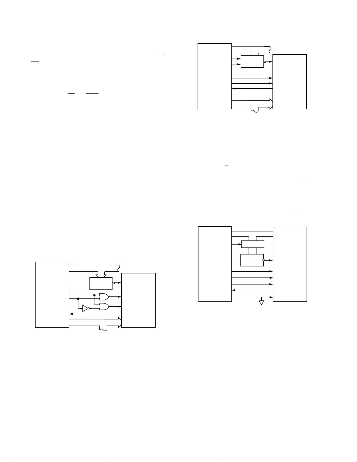
AD7859/AD7859L
DSP56000/
DSP56002*
CS
DB15–DB0
AD7859/
AD7859L*
*ADDITIONAL PINS OMITTED FOR CLARITY
D23–D0
ADDR
DECODE
DS
DATA BUS
WR
RD
ADDRESS BUS
WR
RD
IRQ
A15–A0
X/Y
BUSY
8051*
ADDR
DECODE
CS
DB7–DB0
AD7859/
AD7859L*
*ADDITIONAL PINS OMITTED FOR CLARITY
WR
RD
WR
RD
INT0
P0
BUSY
LATCH
ALE
P2.1 DB8/HBEN
W/B
DGND
The parallel interface on the AD7859/AD7859L is fast enough
to interface to the TMS32020 with no extra wait states. If high
speed glue logic such as 74AS devices are used to drive the
and
RD lines when interfacing to the TMS320C25, then again
no wait states are necessary. However, if slower logic is used,
data accesses may be slowed sufficiently when reading from and
writing to the part to require the insertion of one wait state. In
such a case, this wait state can be generated using the single OR
gate to combine the
CS and MSC signals to drive the READY
line of the TMS320C25, as shown in Figure 39. Extra wait
states will be necessary when using the TMS320C5x at their
fastest clock speeds. Wait states can be programmed via the
IOWSR and CWSR registers (please see TMS320C5x User
Guide for details).
Data is read from the ADC using the following instruction:
IN D,ADC
where D is the memory location where the data is to be stored
and ADC is the I/O address of the AD7859/AD7859L.
AD7859/AD7859L to TMS320C30
Figure 40 shows a parallel interface between the AD7859/
AD7859L and the TMS320C3x family of DSPs. The AD7859/
AD7859L is interfaced to the Expansion Bus of the TMS320C3x.
A single wait state is required in this interface. This can be programmed using the WTCNT bits of the Expansion Bus Control
register (see TMS320C3x Users Guide for details). Data from
the AD7859/AD7859L can be read using the following instruction:
LDI *ARn,Rx
where ARn is an auxiliary register containing the lower 16 bits
of the address of the AD7859/AD7859L in the TMS320C3x
memory space and Rx is the register into which the ADC data is
loaded.
WR
Figure 41. AD7859/AD7859L to DSP5600x Parallel Interface
Interfacing the AD7859/AD7859L to an 8-Bit Data Bus
AD7859/AD7859L to 8051
This mode of operation allows the AD7859/AD7859L to be interfaced directly to microcontrollors with an 8-bit data bus. The
AD7859/AD7859L is placed in byte mode by placing a logic
low signal on the W/
B pin.
Figure 42 shows a parallel interface between the AD7859/
AD7859L and the 8051 microcontroller. Here the W/
B pin is
tied logic low and the DB8/HBEN pin connected to line 1 of
Port 2. Port 0 serves as a multiplexed address/data bus to the
AD7859/AD7859L. Alternatively if the 8051 is not using external memory or other memory mapped peripheral devices, line 2
of Port 2 (or any other line) could be used as the
CS signal.
XA12–XA0
TMS320C30*
IOSTRB
XR/W
INTx
XD23–XD0
*ADDITIONAL PINS OMITTED FOR CLARITY
Figure 40. AD7859/AD7859L to TMS320C30 Parallel Interface
AD7859/AD7859L to DSP5600x
Figure 41 shows a parallel interface between the AD7859/
AD7859L and the DSP5600x series of DSPs. The AD7859/
AD7859L should be mapped into the top 64 locations of Y data
memory. If extra wait states are needed in this interface, they
can be programmed using the Port A Bus Control Register
(please see DSP5600x Users Manual for details). Data can be
read from the AD7859/AD7859L using the following instruction:
where ADC is the address in the DSP5600x address space
which the AD7859/AD7859L has been mapped to.
EXPANSION ADDRESS BUS
ADDR
DECODE
EXPANSION DATA BUS
MOVEO Y:ADC,X0
CS
AD7859/
AD7859L*
WR
RD
BUSY
DB15–DB0
Figure 42. AD7859/AD7859L to 8051 Parallel Interface
APPLICATION HINTS
Grounding and Layout
The analog and digital supplies of the AD7859/AD7859L are
independent and separately pinned out to minimize coupling
between the analog and digital sections of the device. The part
has very good immunity to noise on the power supplies as can
be seen by the PSRR versus Frequency graph. However, care
should still be taken with regard to grounding and layout.
The printed circuit board on which the AD7859/AD7859L is
mounted should be designed such that the analog and digital
sections are separated and confined to certain areas of the
board. This facilitates the use of ground planes that can be easily separated. A minimum etch technique is generally best for
ground planes as it gives the best shielding. Digital and analog
ground planes should only be joined in one place. If the
AD7859/AD7859L is the only device requiring an AGND to
–26–
REV. A

AD7859/AD7859L
DGND connection, then the ground planes should be connected at the AGND and DGND pins of the AD7859/
AD7859L. If the AD7859/AD7859L is in a system where multiple devices require AGND to DGND connections, the connection should still be made at one point only, a star ground
point which should be established as close as possible to the
AD7859/AD7859L.
Avoid running digital lines under the device as these couple
noise onto the die. The analog ground plane should be allowed
to run under the AD7859/AD7859L to avoid noise coupling.
The power supply lines to the AD7859/AD7859L should use as
large a trace as possible to provide low impedance paths and
reduce the effects of glitches on the power supply line. Fast
switching signals like clocks and the data inputs should be
shielded with digital ground to avoid radiating noise to other
sections of the board and clock signals should never be run near
the analog inputs. Avoid crossover of digital and analog signals.
Traces on opposite sides of the board should run at right angles
to each other. This reduces the effects of feedthrough through
the board. A microstrip technique is by far the best but is not always possible with a double-sided board. In this technique, the
component side of the board is dedicated to ground planes
while signals are placed on the solder side.
Good decoupling is also important. All analog supplies should
be decoupled with a 10 µF tantalum capacitor in parallel with
0.1 µF disc ceramic capacitor to AGND. All digital supplies
should have a 0.1 µF disc ceramic capacitor to DGND. To
achieve the best performance from these decoupling components, they must be placed as close as possible to the device,
ideally right up against the device. In systems where a common
supply voltage is used to drive both the AV
AD7859/AD7859L, it is recommended that the system’s AV
and DVDD of the
DD
DD
supply is used. In this case an optional 10 Ω resistor between
the AV
pin and DVDD pin can help to filter noise from digital
DD
circuitry. This supply should have the recommended analog
supply decoupling capacitors between the AV
pin of the
DD
AD7859/AD7859L and AGND and the recommended digital
supply decoupling capacitor between the DV
pin of the
DD
AD7859/AD7859L and DGND.
Evaluating the AD7859/AD7859L Performance
The recommended layout for the AD7859/AD7859L is outlined
in the evaluation board for the AD7859/AD7859L. The evaluation board package includes a fully assembled and tested evaluation board, documentation, and software for controlling the
board from the PC via the EVAL-CONTROL BOARD. The
EVAL-CONTROL BOARD can be used in conjunction with
the AD7859/AD7859L Evaluation board, as well as many other
Analog Devices evaluation boards ending in the CB designator,
to demonstrate/evaluate the ac and dc performance of the
AD7859/AD7859L.
The software allows the user to perform ac (fast Fourier transform) and dc (histogram of codes) tests on the AD7859/
AD7859L. It also gives full access to all the AD7859/AD7859L
on-chip registers allowing for various calibration and powerdown options to be programmed.
AD785x Family
All parts are 12 bits, 200 kSPS, 3.0 V to 5.5 V.
AD7853 – Single-Channel Serial
AD7854 – Single-Channel Parallel
AD7858 – Eight-Channel Serial
AD7859 – Eight-Channel Parallel
REV. A
–27–

PAGE INDEX
Topic Page
FEATURES . . . . . . . . . . . . . . . . . . . . . . . . . . . . . . . . . . . . . . . . 1
GENERAL DESCRIPTION . . . . . . . . . . . . . . . . . . . . . . . . . . . 1
PRODUCT HIGHLIGHTS . . . . . . . . . . . . . . . . . . . . . . . . . . . . 1
SPECIFICATIONS . . . . . . . . . . . . . . . . . . . . . . . . . . . . . . . . . . 2
TIMING SPECIFICATIONS . . . . . . . . . . . . . . . . . . . . . . . . . . 4
ABSOLUTE MAXIMUM RATINGS . . . . . . . . . . . . . . . . . . . . 5
ORDERING GUIDE . . . . . . . . . . . . . . . . . . . . . . . . . . . . . . . . . 5
PINOUTS . . . . . . . . . . . . . . . . . . . . . . . . . . . . . . . . . . . . . . . . . . 5
TERMINOLOGY . . . . . . . . . . . . . . . . . . . . . . . . . . . . . . . . . . . . 6
PIN FUNCTION DESCRIPTION . . . . . . . . . . . . . . . . . . . . . . 7
AD7859/AD7859L ON-CHIP REGISTERS . . . . . . . . . . . . . . . 8
Addressing the On-Chip Registers . . . . . . . . . . . . . . . . . . . . . . 8
Writing/Reading . . . . . . . . . . . . . . . . . . . . . . . . . . . . . . . . . . . . 8
CONTROL REGISTER . . . . . . . . . . . . . . . . . . . . . . . . . . . . . . . 9
STATUS REGISTER . . . . . . . . . . . . . . . . . . . . . . . . . . . . . . . . 11
CALIBRATION REGISTERS . . . . . . . . . . . . . . . . . . . . . . . . . 12
Addressing the Calibration Registers . . . . . . . . . . . . . . . . . . . 12
Writing to/Reading from the Calibration Registers . . . . . . . . 12
Adjusting the Offset Calibration Register . . . . . . . . . . . . . . . . 13
Adjusting the Gain Calibration Registers . . . . . . . . . . . . . . . . 13
CIRCUIT INFORMATION . . . . . . . . . . . . . . . . . . . . . . . . . . 14
CONVERTER DETAILS . . . . . . . . . . . . . . . . . . . . . . . . . . . . 14
TYPICAL CONNECTION DIAGRAM . . . . . . . . . . . . . . . . . 14
ANALOG INPUT . . . . . . . . . . . . . . . . . . . . . . . . . . . . . . . . . . 15
Acquisition Time . . . . . . . . . . . . . . . . . . . . . . . . . . . . . . . . . . 15
DC/AC Applications . . . . . . . . . . . . . . . . . . . . . . . . . . . . . . 15
Input Ranges . . . . . . . . . . . . . . . . . . . . . . . . . . . . . . . . . . . . 16
Transfer Functions . . . . . . . . . . . . . . . . . . . . . . . . . . . . . . . 16
REFERENCE SECTION . . . . . . . . . . . . . . . . . . . . . . . . . . . . . 17
AD7859/AD7859L PERFORMANCE CURVES . . . . . . . . . . 17
POWER-DOWN OPTIONS . . . . . . . . . . . . . . . . . . . . . . . . . . 18
POWER-UP TIMES . . . . . . . . . . . . . . . . . . . . . . . . . . . . . . . . 18
POWER VS. THROUGHPUT RATE . . . . . . . . . . . . . . . . . . 19
CALIBRATION SECTION . . . . . . . . . . . . . . . . . . . . . . . . . . 21
Calibration Overview . . . . . . . . . . . . . . . . . . . . . . . . . . . . . . . 21
Calibration on Power-On . . . . . . . . . . . . . . . . . . . . . . . . . . . . 21
Self-Calibration Description . . . . . . . . . . . . . . . . . . . . . . . . . 21
Self-Calibration Timing . . . . . . . . . . . . . . . . . . . . . . . . . . . . . 22
System Calibration Description . . . . . . . . . . . . . . . . . . . . . . . 22
System Gain and Offset Interaction . . . . . . . . . . . . . . . . . . . . 23
System Calibration Timing . . . . . . . . . . . . . . . . . . . . . . . . . . 23
PARALLEL INTERFACE . . . . . . . . . . . . . . . . . . . . . . . . . . . 24
MICROPROCESSOR INTERFACING . . . . . . . . . . . . . . . . 25
APPLICATIONS HINTS . . . . . . . . . . . . . . . . . . . . . . . . . . . . . 27
Grounding and Layout . . . . . . . . . . . . . . . . . . . . . . . . . . . . . 27
Evaluating the AD7859/AD7859L Performance . . . . . . . . . . 27
INDEX . . . . . . . . . . . . . . . . . . . . . . . . . . . . . . . . . . . . . . . . . . . 28
OUTLINE DIMENSIONS . . . . . . . . . . . . . . . . . . . . . . . . . . . 28
0.048 (1.21)
0.042 (1.07)
0.020
(0.50)
R
0.037 (0.95)
0.026 (0.65)
0.398 (10.1)
0.390 (9.9)
0.040 (1.02)
0.032 (0.82)
OUTLINE DIMENSIONS
Dimensions shown in inches and (mm).
44-Lead PLCC
(P-44A)
7
17
0.048 (1.21)
0.042 (1.07)
6
18
PIN 1
IDENTIFIER
TOP VIEW
0.656 (16.66)
0.650 (16.51)
0.695 (17.65)
0.685 (17.40)
0.056 (1.42)
0.042 (1.07)
40
39
29
28
SQ
SQ
44-Pin PQFP
(S-44)
0.096 (2.45)
MAX
8°
0.083 (2.1)
0.077 (1.95)
0°
0.040 (1.02)
0.032 (0.82)
33
34
44
1
0.016 (0.4)
0.012 (0.3)
PIN 1
0.180 (4.57)
0.165 (4.19)
0.110 (2.79)
0.085 (2.16)
0.557 (14.15)
0.537 (13.65)
0.397 (10.1)
0.390 (9.9)
TOP VIEW
0.025 (0.63)
0.015 (0.38)
0.021 (0.53)
0.013 (0.33)
0.032 (0.81)
0.026 (0.66)
0.050
(1.27)
BSC
0.040 (1.01)
0.025 (0.64)
0.033 (0.85)
0.029 (0.75)
0.63 (16.00)
0.59 (14.99)
23
22
12
11
C2109–7–1/96
PRINTED IN U.S.A.
–28–
 Loading...