Analog Devices AD7849TQ, AD7849CR, AD7849CN, AD7849BR, AD7849BN Datasheet
...
REV. B
Information furnished by Analog Devices is believed to be accurate and
reliable. However, no responsibility is assumed by Analog Devices for its
use, nor for any infringements of patents or other rights of third parties
which may result from its use. No license is granted by implication or
otherwise under any patent or patent rights of Analog Devices.
a
Serial Input,
14-Bit/16-Bit DAC
AD7849*
FEATURES
14-Bit/16-Bit Multiplying DAC
Guaranteed Monotonicity
Output Control on Power-Up and Power-Down
Internal or External Control
Versatile Serial Interface
DAC Clears to 0 V in Both Unipolar and Bipolar Output
Ranges
APPLICATIONS
Industrial Process Control
PC Analog I/O Boards
Instrumentation
GENERAL DESCRIPTION
The AD7849 is a 14-bit/16-bit serial input multiplying DAC.
The DAC architecture ensures excellent differential linearity
performance, and monotonicity is guaranteed to 14 bits for the
A grade and to 16 bits for all other grades over the specified
temperature ranges.
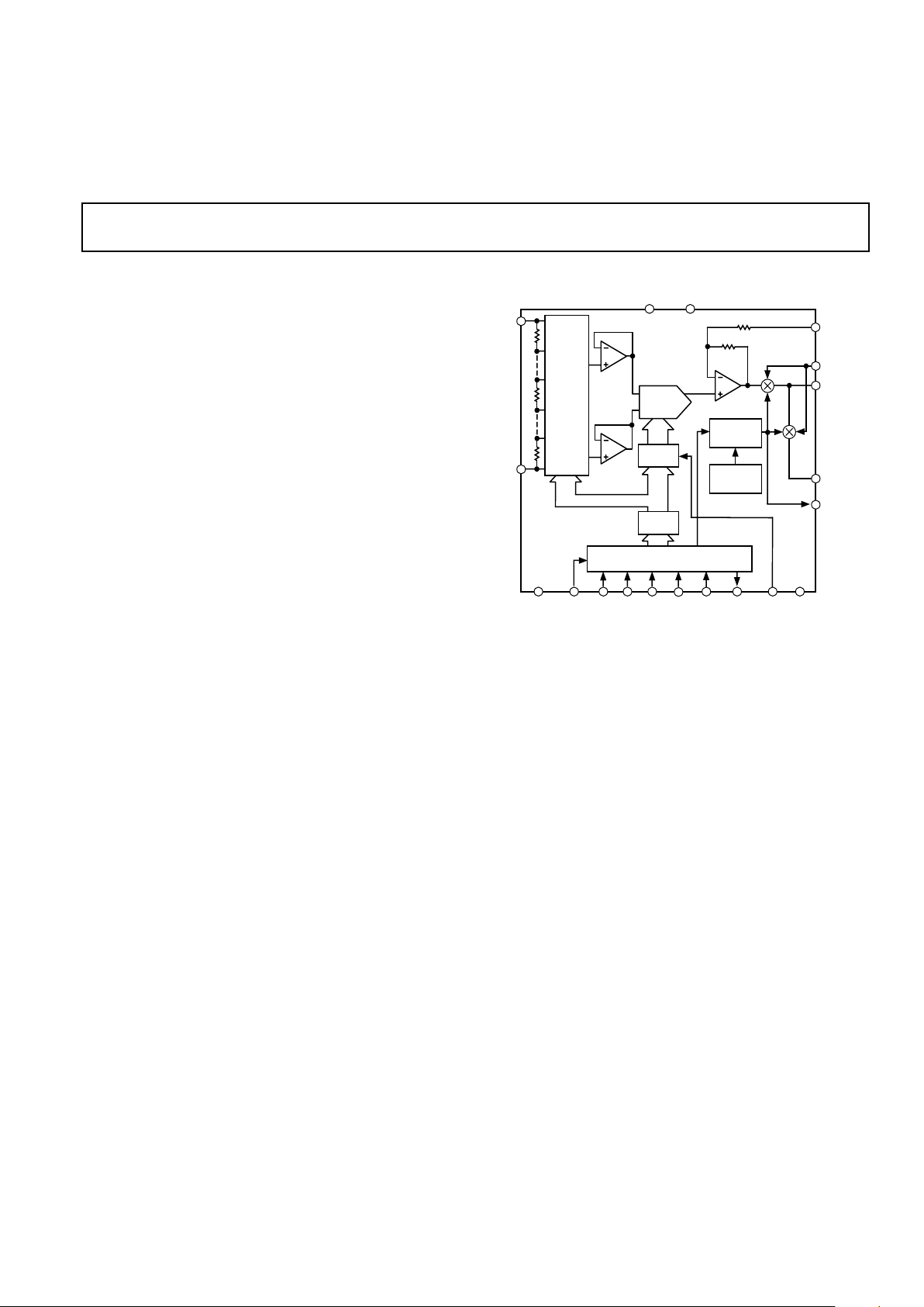
During power-up and power-down sequences (when the supply
voltages are changing), the V
OUT
pin is clamped to 0 V via a low
impedance path. To prevent the output of A3 being shorted to
0 V during this time, transmission gate G1 is also opened.
These conditions are maintained until the power supplies
stabilize and a valid word is written to the DAC register. At this
time, G2 opens and G1 closes. Both transmission gates are also
externally controllable via the Reset In (RST IN) control input.
For instance, if the RST IN input is driven from a battery supervisor chip, then on power-off or during a brown out, the RST
IN input will be driven low to open G1 and close G2. The DAC
must be reloaded, with RST IN high, to re-enable the output.
Conversely, the on-chip voltage detector output (RST OUT) is
also available to the user to control other parts of the system.
FUNCTIONAL BLOCK DIAGRAM
V
DDVCC
R
R
R
R
R
AD7849
R
OFS
RST IN
V
OUT
AGND
RST OUT
G1
G2
SDIN SCLK
SYNC CLR BIN/
COMP
DCEN SDOUT
LDAC
V
SS
DGND
DAC
LATCH
10/
12
10/
12
10-BIT/
12-BIT
DAC
A1
A2
16-
SEG-
MENT
SWITCH
MATRIX
4
V
REF+
V
REF–
A3
LOGIC
CIRCUITRY
VOLTAGE
MONITOR
INPUT
LATCH
INPUT SHIFT REGISTER/
CONTROL LOGIC
The AD7849 has a versatile serial interface structure and can be
controlled over three lines to facilitate opto-isolator applications.
SDOUT is the output of the on-chip shift register and can be
used in a daisy-chain fashion to program devices in the multichannel system. The DCEN (Daisy Chain Enable) input controls this function.
The BIN/COMP pin sets the DAC coding; with BIN/COMP
set to 0, the coding is straight binary; and with it set to 1, the
coding is 2s complement. This allows the user to reset the DAC
to 0 V in both the unipolar and bipolar output ranges.
The part is available in a 20-lead DIP and 20-lead SOIC package.
*Protected by U.S. Patent No. 5,319,371.
One Technology Way, P.O. Box 9106, Norwood, MA 02062-9106, U.S.A.
Tel: 781/329-4700 World Wide Web Site: http://www.analog.com
Fax: 781/326-8703 © Analog Devices, Inc., 2000

AB, TC
Parameter Versions Versions Versions Units Test Conditions/Comments
RESOLUTION 14 16 16 Bits A Versions: 1 LSB = 2 (V
REF+–VREF–
)/2
14
B, C, T Versions: 1 LSB = 2 (V
REF+–VREF–
)/2
16
UNIPOLAR OUTPUT V
REF–
= 0 V, V
OUT
= 0 V to +10 V
Relative Accuracy @ +25°C ±4 ±6 ±4 LSBs typ
T
MIN
to T
MAX
±5 ±16 ±8 LSBs max
Differential Nonlinearity ±0.25 ±0.9 ±0.5 LSBs max All Grades Guaranteed Monotonic Over Temperature
Gain Error @ +25°C ±1 ± 4 ± 4 LSBs typ V
OUT
Load = 10 MΩ
T
MIN
to T
MAX
±4 ±16 ±16 LSBs max
Offset Error @ +25°C ±1 ±4 ±4 LSBs typ
T
MIN
to T
MAX
±6 ±24 ±16 LSBs max
Gain TC
3
±2 ±2 ±2 ppm FSR/°C typ
Offset TC
3
±2 ±2 ±2 ppm FSR/°C typ
BIPOLAR OUTPUT V
REF–
= –5 V, V
OUT
= –10 V to +10 V
Relative Accuracy @ +25°C ±2 ±3 ±2 LSBs typ
T
MIN
to T
MAX
±3 ±8 ±4 LSBs max
Differential Nonlinearity ±0.25 ±0.9 ±0.5 LSBs max All Grades Guaranteed Monotonic Over Temperature
Gain Error @ +25°C ±1 ± 4 ± 4 LSBs typ V
OUT
Load = 10 MΩ
T
MIN
to T
MAX
±4 ±16 ±16 LSBs max
Offset Error @ +25°C ±0.5 ±2 ±2 LSBs typ
T
MIN
to T
MAX
±3 ±12 ±8 LSBs max
Bipolar Zero Error @ +25°C ±0.5 ±2 ±2 LSBs typ
T
MIN
to T
MAX
±4 ±12 ±8 LSBs max
Gain TC
3
±2 ±2 ±2 ppm FSR/°Ctyp
Offset TC
3
±2 ±2 ±2 ppm FSR/°Ctyp
Bipolar Zero TC
3
±2 ±2 ±2 ppm FSR/°Ctyp
REFERENCE INPUT
Input Resistance 25 25 25 kΩ min Resistance from V
REF+
to V
REF–
43 43 43 kΩ max Typically 34 kΩ
V
REF+
Range VSS + 6 to VSS + 6 to VSS + 6 to Volts
VDD – 6 VDD – 6 VDD – 6
V
REF–
Range VSS + 6 to VSS + 6 to VSS + 6 to Volts
VDD – 6 VDD – 6 VDD – 6
OUTPUT CHARACTERISTICS
Output Voltage Swing VSS + 4 to VSS + 4 to VSS + 4 to V max
VDD – 4 VDD – 4 VDD – 4
Resistive Load 2 2 2 kΩ min To 0 V
Capacitive Load 200 200 200 pF max To 0 V
Output Resistance 0.3 0.3 0.3 Ω typ
Short Circuit Current ± 25 ± 25 ± 25 mA typ Voltage Range: –10 V to +10 V
DIGITAL INPUTS
V
INH
, Input High Voltage 2.4 2.4 2.4 V min
V
INL
, Input Low Voltage 0.8 0.8 0.8 V max
I
INH
, Input Current ±10 ±10 ±10 µA max
CIN, Input Capacitance 10 10 10 pF max
DIGITAL OUTPUTS
VOL (Output Low Voltage) 0.4 0.4 0.4 Volts max I
SINK
= 1.6 mA
VOH (Output High Voltage) 4.0 4.0 4.0 Volts min I
SOURCE
= 400 µA
Floating State Leakage Current ±10 ±10 ±10 µA max
Floating State Output
Capacitance 10 10 10 pF max
POWER REQUIREMENTS
4
V
DD
+14.25/+15.75 +14.25/+15.75 +14.25/+15.75 V min/V max
V
SS
–14.25/–15.75 –14.25/–15.75 –14.25/–15.75 V min/V max
V
CC
+4.75/+5.25 +4.75/+5.25 +4.75/+5.25 V min/V max
I
DD
5 5 5 mA max V
OUT
Unloaded, V
INH
= VDD – 0.1 V, V
INL
= 0.1 V
I
SS
5 5 5 mA max V
OUT
Unloaded, V
INH
= VDD – 0.1 V, V
INL
= 0.1 V
I
CC
2.5 2.5 2.5 mA max V
INH
= VDD – 0.1 V, V
INL
= 0.1 V
Power Supply Sensitivity
5
0.4 1.5 1.5 LSB/V max
Power Dissipation 100 100 100 mW typ V
OUT
Unloaded
NOTES
1
Temperature ranges: A, B, C Versions: –40°C to +85°C; T Version: –55°C to +125°C.
2
Minimum load for T Version is 3 kΩ.
3
Guaranteed by design and characterization, not production tested.
4
The AD7849 is functional with power supplies of ± 12 V. See Typical Performance Curves.
5
Sensitivity of Gain Error, Offset Error and Bipolar Zero Error to VDD, VSS variations.
Specifications subject to change without notice.
AD7849–SPECIFICATIONS
1
REV. B
–2–
(V
DD
= +14.25 V to +15.75 V; VSS = –14.25 V to –15.75 V; VCC = +4.75 V to +5.25 V; V
OUT
loaded with 2 kΩ,2 200 pF to 0 V; V
REF+
= +5 V;
R
OFS
connected to 0 V; TA = T
MIN
to T
MAX
, unless otherwise noted)

Limit at +25ⴗC Limit at T
MIN
, T
MAX
Parameter (All Versions) (All Versions) Units Conditions/Comments
t
1
3
200 200 ns min SCLK Cycle Time
t
2
50 50 ns min SYNC to SCLK Setup Time
t
3
70 70 ns min SYNC to SCLK Hold Time
t
4
10 10 ns min Data Setup Time
t
5
40 40 ns min Data Hold Time
t
6
4
80 80 ns max SCLK Falling Edge to SDO Valid
t
7
80 80 ns min LDAC, CLR Pulsewidth
t
r
30 30 µs max Digital Input Rise Time
t
f
30 30 µs max Digital Input Fall Time
NOTES
1
Guaranteed by characterization.
2
All input signals are specified with tr = tf = 5 ns (10% to 90% of 5 V) and timed from a voltage level of 1.6 V.
3
SCLK mark/space ratio range is 40/60 to 60/40.
4
SDO load capacitance is 50 pF.
Specification subject to change without notice.
AD7849
REV. B
–3–
RESET SPECIFICATIONS
(These specifications apply when the device goes into the Reset mode during a power-up or
power-down sequence.) V
OUT
unloaded.
Parameter All Versions Units Test Conditions/Comments
V
A
1
, Low Threshold Voltage for VDD, VSS1.2 Volt max This is the lower VDD/VSS threshold voltage for the reset
0 Volts typ function. Above this, the reset is activated.
V
B
, High Threshold Voltage for VDD, VSS9.5 Volts max This is the higher VDD/V
SS
threshold voltage for the reset
6.4 Volts min function. Below this, the reset is activated. Typically 8 volts.
V
C
, Low Threshold Voltage for V
CC
1 Volt max This is the lower threshold voltage for the reset function.
0 Volts typ Above this, the reset is activated.
V
D
, High Threshold Voltage for V
CC
4 Volts max This is the higher VCC threshold voltage for the reset function.
2.5 Volts min Below this, the reset is activated. Typically 3 volts.
G2 R
ON
1kΩ typ On Resistance of G2; VDD = 2 V; VSS = –2 V; IG2 = 1 mA.
NOTES
1
A pull-down resistor (65 kΩ) on V
OUT
maintains 0 V output when VDD/VSS is below VA.
Specifications subject to change without notice.
TIMING CHARACTERISTICS
1, 2
(V
DD
= +14.25 V to +15.75 V; V
SS
= –14.25 V to –15.75 V; VCC = +4.75 V to +5.25 V;
RL = 2 kΩ, CL = 200 pF. All Specifications T
MIN
to T
MAX
unless otherwise noted.)
AC PERFORMANCE CHARACTERISTICS
(These characteristics are included for Design Guidance and are not
subject to test. (V
REF+
= +5 V; VDD= +14.25 V to +15.75 V; VSS= –14.25 V to –15.75 V; VCC= +4.75 V to +5.25 V; R
OFS
connected to 0 V.)
T A, B, C
Parameter Version Versions Units Test Conditions/Comments
DYNAMIC PERFORMANCE
Output Settling Time
1
77µs typ To 0.006% FSR. V
OUT
Loaded. V
REF–
= 0 V.
10 10 µs typ To 0.003% FSR. V
OUT
Loaded. V
REF–
= –5 V.
Slew Rate 4 4 V/µs typ
Digital-to-Analog Glitch Impulse 250 250 nV-s typ DAC Alternately Loaded with 00 . . . 00 and
111 . . . 11. V
OUT
Unloaded. LDAC Perma-
nently Low. BIN/COMP Set to 1. V
REF–
= –5 V.
150 150 nV-s typ LDAC Frequency = 100 kHz
AC Feedthrough 1 1 mV pk-pk typ V
REF–
= 0 V, V
REF+
= 1 V rms, 10 kHz Sine Wave.
DAC Loaded with All 0s. BIN/COMP Set to 0.
Digital Feedthrough 5 5 nV-s typ DAC Alternately Loaded with All 1s and All 0s.
SYNC High.
Output Noise Voltage Density
1 kHz–100 kHz 80 80 nV/√Hz typ Measured at V
OUT
. V
REF+
= V
REF–
= 0 V.
BIN/COMP Set to 0.
NOTES
1
LDAC = 0. Settling time does not include deglitching time of 5 µs (typ).
Specification subject to change without notice.

REV. B
–4–
AD7849
ABSOLUTE MAXIMUM RATINGS
1
(TA = +25°C unless otherwise noted)
VDD to DGND . . . . . . . . . . . . . . . . . . . . . . . . . –0.4 V to +17 V
V
CC
to DGND2 . . . . . . . . . . . . . . . . . . –0.4 V, VDD + 0.4 V or
+7 V (Whichever Is Lower)
V
SS
to DGND . . . . . . . . . . . . . . . . . . . . . . . . . –0.4 V to –17 V
V
REF+
to DGND . . . . . . . . . . . . . . . . VDD + 0.4 V, VSS – 0.4 V
V
REF–
to DGND . . . . . . . . . . . . . . . . VDD + 0.4 V, VSS – 0.4 V
V
OUT
to DGND3 . . . . . . . . . . . . . . VDD + 0.4 V, VSS – 0.4 V or
±10 V (Whichever Is Lower)
R
OFS
to DGND . . . . . . . . . . . . . . . . . VDD + 0.4 V, VSS – 0.4 V
Digital Input Voltage to DGND . . . . . . –0.4 V to V
CC
+ 0.4 V
Input Current to any Pin Except Supplies
4
. . . . . . . . . ± 10 mA
Operating Temperature Range
Commercial/Industrial (A, B, C Versions). . . . –40°C to +85°C
Extended (T Version) . . . . . . . . . . . . . . . .–55°C to +125°C
Storage Temperature Range . . . . . . . . . . . . . –65°C to +150°C
Junction Temperature . . . . . . . . . . . . . . . . . . . . . . . . . +150°C
Plastic DIP Package, Power Dissipation . . . . . . . . . . . 875 mW
θ
JA
Thermal Impedance . . . . . . . . . . . . . . . . . . . . . 102°C/W
Lead Temperature (Soldering, 10 secs) . . . . . . . . . . +260° C
SOP Package, Power Dissipation . . . . . . . . . . . . . . . . .875 mW
θ
JA
Thermal Impedance . . . . . . . . . . . . . . . . . . . . . . 74°C/W
Lead Temperature, Soldering
Vapor Phase (60 secs) . . . . . . . . . . . . . . . . . . . . . . +215°C
Infrared (15 secs) . . . . . . . . . . . . . . . . . . . . . . . . . +220°C
Cerdip Package, Power Dissipation . . . . . . . . . . . . . . . 875 mW
θ
JA
Thermal Impedance . . . . . . . . . . . . . . . . . . . . . . 71°C/W
Lead Temperature, Soldering (Soldering 10 secs) . . . 260°C
NOTES
1
Stresses above those listed under Absolute Maximum Ratings may cause permanent damage to the device. This is a stress rating only; functional operation of the
device at these or any other conditions above those listed in the operational sections
of this specification is not implied. Exposure to absolute maximum rating
conditions for extended periods may affect device reliability.
2
VCC must not exceed VDD by more than 0.4 V. If it is possible for this to happen
during power-up or power-down (for example, if V
CC
is greater than +0.4 V while
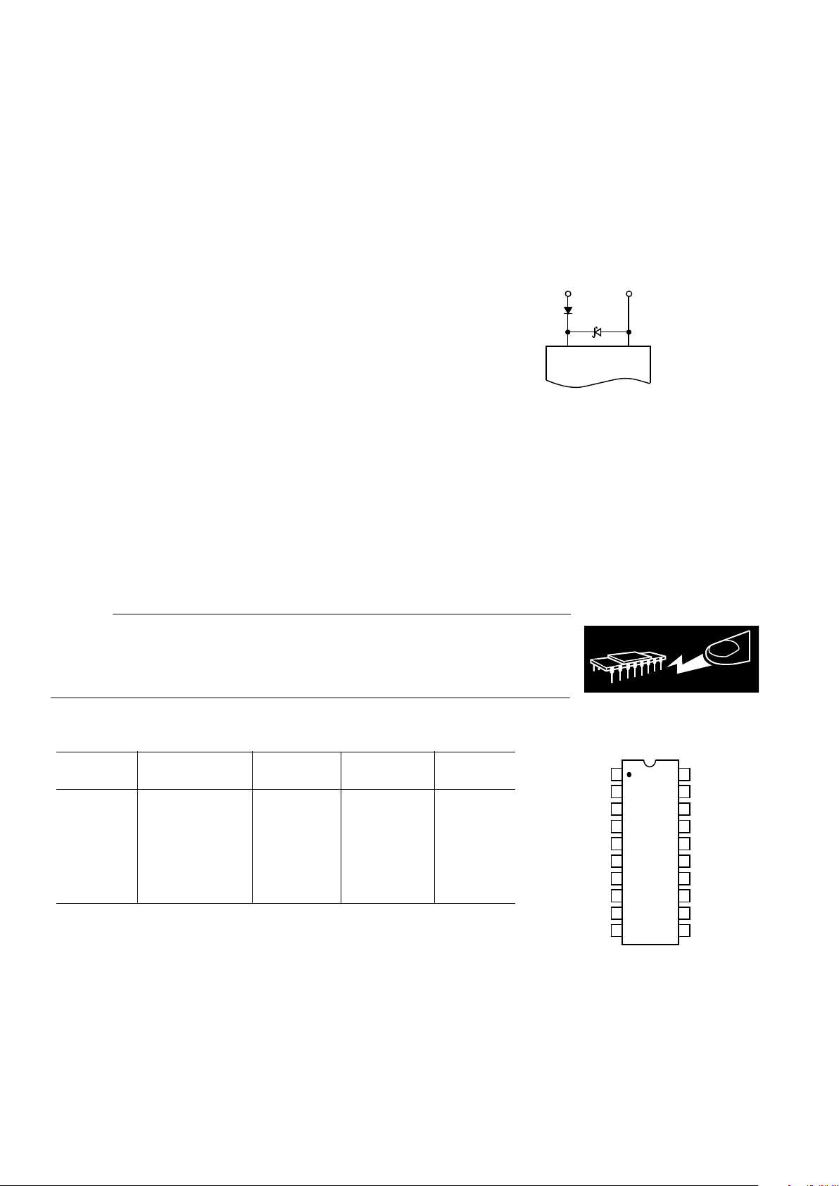
VDD is still 0 V), the following diode protection scheme will ensure protection.
SD103C
1N5711
1N5712
1N4148
V
DD
V
CC
V
DD
V
CC
AD7849
3
V
OUT
may be shorted to DGND, +10 V, –10 V, provided that the power dissipation
of the package is not exceeded.
4
Transient currents of up to 100 mA will not cause SCR latch-up.
CAUTION
ESD (electrostatic discharge) sensitive device. Electrostatic charges as high as 4000 V readily
accumulate on the human body and test equipment and can discharge without detection.
Although the AD7849 features proprietary ESD protection circuitry, permanent damage may
occur on devices subjected to high energy electrostatic discharges. Therefore, proper ESD
precautions are recommended to avoid performance degradation or loss of functionality.
ORDERING GUIDE
Temperature Resolution Bipolar Package
Model Range (Bits) INL (LSBs) Option
*
AD7849AN –40°C to +85°C14 ± 3 N-20
AD7849BN –40°C to +85°C16 ± 8 N-20
AD7849CN –40°C to +85°C16 ±4 N-20
AD7849AR –40°C to +85°C14 ± 3 R-20
AD7849BR –40°C to +85°C16 ± 8 R-20
AD7849CR –40°C to +85°C16 ± 4 R-20
AD7849TQ –55°C to +125°C16 ± 8 Q-20
*N = Plastic DIP; R = SOP (Small Outline Package); Q = Cerdip.
PIN CONFIGURATION
14
13
12
11
17
16
15
20
19
18
10
9
8
1
2
3
4
7
6
5
TOP VIEW
(Not to Scale)
AD7849
NC = NO CONNECT
V
REF+
V
DD
NC
V
OUT
R
OFS
V
REF–
V
SS
SYNC
RSTIN
RSTOUT
AGND
SCLK
V
CC
SDOUT
DCEN
BIN/COMP
DGND
LDAC
SDIN
CLR
WARNING!
ESD SENSITIVE DEVICE

AD7849
REV. B
–5–
TERMINOLOGY
Least Significant Bit
This is the analog weighting of 1 bit of the digital word in a DAC.
For the AD7849, B, C and T versions, 1 LSB = (V
REF+–VREF–
)/
2
16
. For the AD7849, A version, 1 LSB = (V
REF+
– V
REF–
)/214.
Relative Accuracy
Relative accuracy or endpoint nonlinearity is a measure of the
maximum deviation from a straight line passing through the
endpoints of the DAC transfer function. It is measured after
adjusting for both endpoints (i.e., offset and gain errors are adjusted out) and is normally expressed in least significant bits or
as a percentage of full-scale range.
Differential Nonlinearity
Differential nonlinearity is the difference between the measured
change and the ideal change between any two adjacent codes. A
specified differential nonlinearity of less than ±1 LSB over the
operating temperature range ensures monotonicity.
Gain Error
Gain error is a measure of the output error between an ideal
DAC and the actual device output with all 1s loaded after offset
error has been adjusted out. Gain error is adjustable to zero
with an external potentiometer.
Offset Error
This is the error present at the device output with all 0s loaded
in the DAC. It is due to op amp input offset voltage and bias
current and the DAC leakage current.
Bipolar Zero Error
When the AD7849 is connected for bipolar output and
(100 . . . 000) is loaded to the DAC, the deviation of the analog
output from the ideal midscale of 0 V, is called the bipolar zero
error.
Digital-to-Analog Glitch Impulse
This is the amount of charge injected from the digital inputs to
the analog output when the inputs change state. This is normally specified as the area of the glitch in nV-secs.
Multiplying Feedthrough Error
This is an ac error due to capacitive feedthrough from either of
the V
REF
terminals to V
OUT
when the DAC is loaded with all 0s.
Digital Feedthrough
When the DAC is not selected (SYNC is held high), high frequency logic activity on the digital inputs is capacitively coupled
through the device to show up as noise on the V
OUT
pin. This
noise is digital feedthrough.
PIN FUNCTION DESCRIPTION
Pin Mnemonic Description
1V
REF+
V
REF+
Input. The DAC is specified for V
REF+
of +5 V. The DAC is fully multiplying so that the V
REF+
range is +5 V to –5 V.
2V
REF–
V
REF–
Input. The DAC is specified for V
REF–
of –5 V. Since the DAC is fully multiplying the V
REF–
range is –5 V to +5 V.
3V
SS
Negative supply for the analog circuitry. This is nominally –15 V.
4 SYNC Data Synchronization Logic Input. When it goes low, the internal logic is initialized in readiness for a new data word.
5 SCLK Serial Clock Logic Input. Data is clocked into the input register on each SCLK falling edge.
6V
CC
Positive supply for the digital circuitry. This is nominally +5 V.
7 SDOUT Serial Data Output. With DCEN at Logic “1,” this output is enabled and the serial data in the input shift register is
clocked out on each rising edge of SCLK.
8 DCEN Daisy-Chain Enable Logic Input. Connect this pin high if a daisy-chain interface is being used, otherwise this pin must be
connect low.
9 BIN/COMP Logic Input. This input selects the data format to be either binary or 2s complement. In the unipolar output range,
natural binary format is selected by connecting the input to a Logic “0.” In the bipolar output range, offset binary is
selected by connecting this input to a Logic “0” and 2s complement is selected by connecting it to a Logic “1.”
10 DGND Digital Ground. Ground reference point for the on-chip digital circuitry.
11 LDAC Load DAC Logic Input. This input updates the DAC output. The DAC output is updated on the falling edge of this
signal or alternatively, if this input is permanently low, an automatic update mode is selected whereby the DAC is updated
on the 16th falling SCLK edge.
12 SDIN Serial Data Input. The 16-bit serial data word is applied to this input.
13 CLR Clear Logic Input. Taking this input low sets V
OUT
to 0 V in both the unipolar output range and the bipolar 2s comple-
ment output range. It sets V
OUT
to V
REF–
in the offset binary bipolar output range.
14 RSTIN Reset Logic Input. This input allows external access to the internal reset logic. Applying a Logic “0” to this input, resets
the DAC output to 0 V. In normal operation it should be tied to Logic “1.”
15 RSTOUT Reset Logic Output. This is the output from the on-chip voltage monitor used in the reset circuit. It may used to control
other system components if desired.
16 AGND This is the analog ground for the device. It is the point to which the output gets shorted in the reset mode.
17 V
DD
Positive supply for the analog circuitry. This is +15 V nominal.
18 NC No Connect. Leave unconnected.
19 V
OUT
DAC Output Voltage Pin.
20 R
OFS
Input to summing resistor of DAC output amplifier. This is used to select output voltage ranges. See Figures 16 to 19
in “APPLYING THE AD7849.”
 Loading...