

2.7 V to 5.5 V, 4.5 s, 8-Bit
a
FEATURES
8-Bit ADC with 4 s Conversion Time
Small Footprint 8-Lead microSOIC Package
Specified Over a –40ⴗC to +125ⴗC Temperature Range
Inherent Track-and-Hold Functionality
Operating Supply Range: 2.7 V to 5.5 V
Specifications at 2.7 V to 5.5 V and 5 V ⴞ 10%
Microcontroller Compatible Serial Interface
Optional Automatic Power-Down
Low Power Operation:
570 W at 10 kSPS Throughput Rate
2.9 mW at 50 kSPS Throughput Rate
Analog Input Range: 0 V to V
Reference Input Range: 0 V to V
“Drop In” Upgrade to 10 Bits Available (AD7810)
APPLICATIONS
Low Power, Hand-Held Portable Applications
Requiring Analog-to-Digital Conversion
with 8-Bit Accuracy, e.g.,
Battery Powered Test Equipment
Battery Powered Communications Systems
REF
DD
ADC in 8-Lead microSOIC/DIP
AD7823
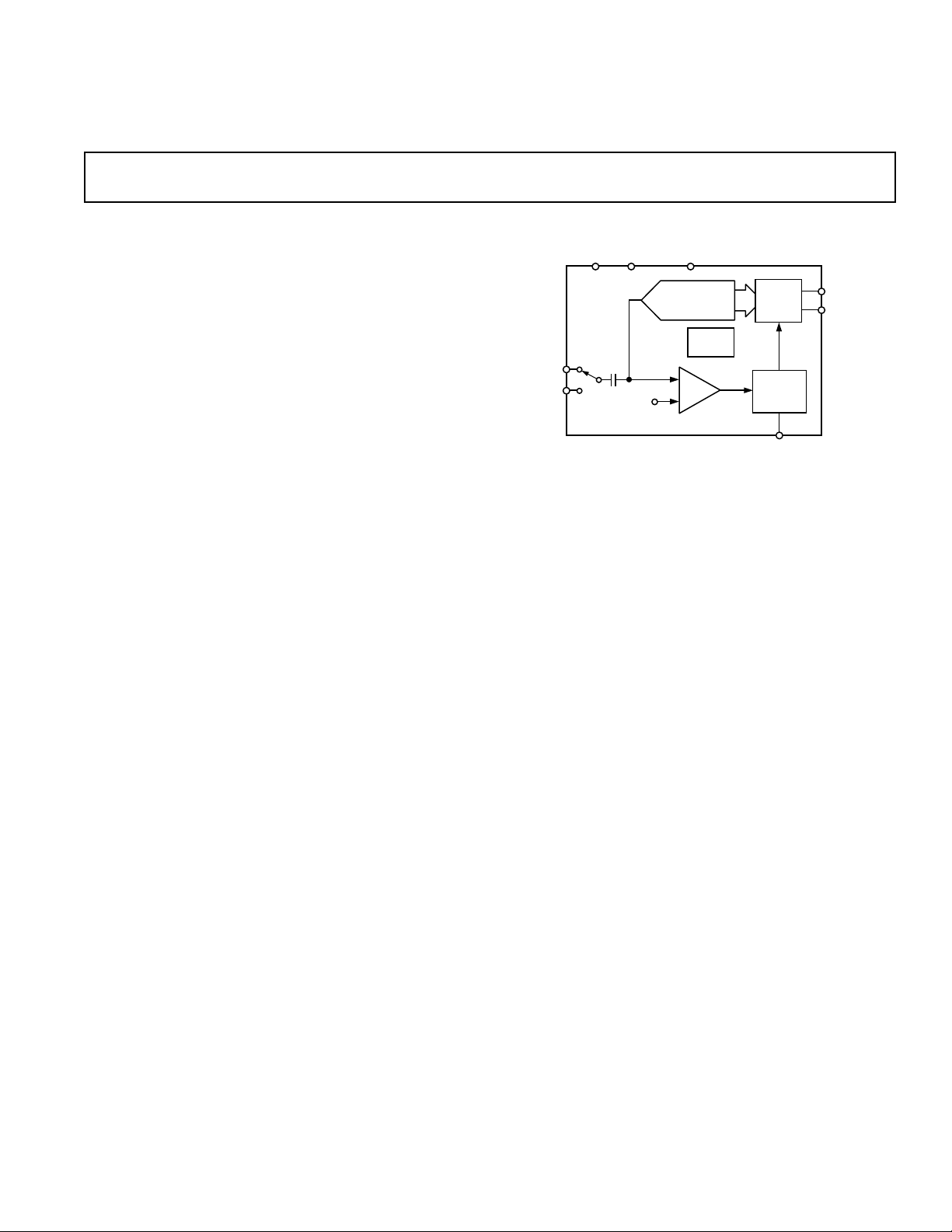
FUNCTIONAL BLOCK DIAGRAM
V
AGND
DD
AD7823
V
IN+
V
IN–
VDD/3
V
REF
CHARGE
REDISTRIBUTION
DAC
CLOCK
OSC
COMP
SERIAL
PORT
CONTROL
LOGIC
CONVST
D
OUT
SCLK
GENERAL DESCRIPTION
The AD7823 is a high speed, low power, 8-bit A/D converter
that operates from a single 2.7 V to 5.5 V supply. The part contains a 4 µs typ successive approximation A/D converter, inherent
track-and-hold functionality (with a pseudo differential input)
and a high speed serial interface that interfaces to most microcontrollers. The AD7823 is fully specified over a temperature range
of –40°C to +125°C.
By using a technique that samples the state of the CONVST
(convert start) signal at the end of a conversion, the AD7823
may be used in an automatic power-down mode. When used in
this mode, the AD7823 powers down automatically at the end
of a conversion and “wakes up” at the start of a new conversion.
This feature significantly reduces the power consumption of the
part at lower throughput rates. The AD7823 can also operate in
a high speed mode where the part is not powered down between
conversions. In this high speed mode of operation, the conversion time of the AD7823 is 4 µs typ. The maximum throughput
rate is dependent on the speed of the serial interface of the
microcontroller.
The part is available in a small, 8-lead 0.3" wide, plastic dualin-line package (mini-DIP); in an 8-lead, small outline IC
(SOIC); and in an 8-lead microSOIC package.
PRODUCT HIGHLIGHTS
1. Complete, 8-Bit ADC in 8-Lead Package
The AD7823 is an 8-bit 4 µs ADC with inherent track-and-
hold functionality and a high speed serial interface—all in an
8-lead microSOIC package. V
may be connected to V
REF
DD
to eliminate the need for an external reference. The result is
a high speed, low power, space saving ADC solution.
2. Low Power, Single Supply Operation
The AD7823 operates from a single +2.7 V to +5.5 V supply
and typically consumes only 9 mW of power. The power
dissipation can be significantly reduced at lower throughput
rates by using the automatic power-down mode, e.g., at a
throughput rate of 10 kSPS the power consumption is only
570 µW.
3. Automatic Power-Down
The automatic power-down mode, whereby the AD7823
“powers down” at the end of a conversion and “wakes up”
before the next conversion, means the AD7823 is ideal for
battery powered applications. See Power vs. Throughput
Rate section.
4. Serial Interface
An easy to use, fast serial interface allows connection to most
popular microprocessors with no external circuitry.
REV. B
Information furnished by Analog Devices is believed to be accurate and
reliable. However, no responsibility is assumed by Analog Devices for its
use, nor for any infringements of patents or other rights of third parties
which may result from its use. No license is granted by implication or
otherwise under any patent or patent rights of Analog Devices.
One Technology Way, P.O. Box 9106, Norwood, MA 02062-9106, U.S.A.
Tel: 781/329-4700 World Wide Web Site: http://www.analog.com
Fax: 781/326-8703 © Analog Devices, Inc., 2000

AD7823–SPECIFICATIONS
(GND = 0 V, V
= +VDD. All specifications –40ⴗC to +125ⴗC unless otherwise noted.)
REF
Parameter Y Version Unit Test Conditions/Comments
DYNAMIC PERFORMANCE f
Signal to (Noise + Distortion) Ratio
Total Harmonic Distortion
Peak Harmonic or Spurious Noise
Intermodulation Distortion
1
2
1, 2
48 dB min
1
–70 dB typ
–70 dB typ
2nd Order Terms –77 dB typ
3rd Order Terms –77 dB typ
DC ACCURACY
Resolution 8 Bits
Relative Accuracy
Differential Nonlinearity (DNL)
Gain Error
Offset Error
Total Unadjusted Error
1
1
1
1
1
± 0.5 LSB max
± 0.5 LSB max
± 1LSB max
± 1LSB max
± 1LSB max
Minimum Resolution for Which
No Missing Codes Are Guaranteed 8 Bits
ANALOG INPUT
Input Voltage Range 0 V min
V max
V max
Input Leakage Current
Input Capacitance
2
REFERENCE INPUTS
V
Input Voltage Range 1.2 V min
REF
V
2
REF
± 1 µA max
15 pF max
2
V
DD
Input Leakage Current ± 1 µA max
Input Capacitance 20 pF max
LOGIC INPUTS
V
Input High Voltage 2.0 V min
INH,
Input Low Voltage 0.4 V max
V
INL,
Input Current, I
Input Capacitance, C
2
IN
IN
± 1 µA max Typically 10 nA, VIN = 0 V to V
8 pF max
LOGIC OUTPUTS
Output High Voltage, V
Output Low Voltage, V
OL
OH
2.4 V min I
0.4 V max I
High Impedance Leakage Current ± 1 µA max
High Impedance Capacitance 15 pF max
= 30 kHz, f
IN
SAMPLE
= 133 kHz
fa = 48 kHz, fb = 48.5 kHz
= 200 µA
SOURCE
= 200 µA
SINK
DD
CONVERSION RATE
Conversion Time 4 µs typ
Track/Hold Acquisition Time
1
100 ns max See DC Acquisition Section
POWER SUPPLY
V
DD
I
DD
2.7–5.5 Volts For Specified Performance
3.5 mA max Sampling at 133 kSPS and Logic
Inputs @ V
DD
Power Dissipation 17.5 mW max Nominal Supplies
Power-Down Mode
I
DD
1 µA max
Power Dissipation 5 µW max Nominal Supplies
Automatic Power Down V
DD
= 3 V
1 kSPS Throughput 54 µW max
10 kSPS Throughput 540 µW max
50 kSPS Throughput 2.7 mW max
NOTES
1
See Terminology.
2
Sample tested during initial release and after any redesign or process change that may affect this parameter.
Specifications subject to change without notice.
–2–
or 0 V. VDD = 5 V
REV. B
1, 2
TIMING CHARACTERISTICS
(–40ⴗC to +125ⴗC, unless otherwise noted)
Parameter VDD = 5 V ⴞ 10% VDD = 3 V ⴞ 10% Unit Conditions/Comments
AD7823
t
1
t
2
t
3
t
4
3
t
5
3
t
6
3
t
7
3, 4
t
8
55µs (max) Conversion Time Mode 1 Operation (High Speed Mode)
20 20 ns (min) CONVST Pulsewidth
25 25 ns (min) SCLK High Pulsewidth
25 25 ns (min) SCLK Low Pulsewidth
5 5 ns (min) CONVST Rising Edge to SCLK Rising Edge Set-Up Time
10 10 ns (max) SCLK Rising Edge to D
Data Valid Delay
OUT
5 5 ns (max) Data Hold Time after Rising Edge SCLK
20 20 ns (max) Bus Relinquish Time After Falling Edge of SCLK
10 10 ns (min)
t
POWERUP
NOTES
1
Sample tested to ensure compliance.
2
See Figures 14, 15 and 16.
3
These numbers are measured with the load circuit of Figure 1. They are defined as the time required for the o/p to cross 0.8 V or 2.4 V for VDD = 5 V ± 10% and
0.4 V or 2 V for VDD = 3 V ± 10%.
4
Derived from the measured time taken by the data outputs to change 0.5 V when loaded with the circuit of Figure 1. The measured number is then extrapolated back
to remove the effects of charging or discharging the 50 pF capacitor. This means that the time quoted in the Timing Characteristics, t8, is the true bus relinquish time
of the part and as such is independent of external bus loading capacitances.
Specifications subject to change without notice.
ABSOLUTE MAXIMUM RATINGS*
(TA = +25°C unless otherwise noted)
V
to GND . . . . . . . . . . . . . . . . . . . . . . . . . . –0.3 V to +7 V
DD
Digital Input Voltage to GND
(CONVST, SCLK) . . . . . . . . . . . . . . –0.3 V, V
Digital Output Voltage to GND
) . . . . . . . . . . . . . . . . . . . . . . . . . –0.3 V, VDD + 0.3 V
(D
OUT
V
to GND . . . . . . . . . . . . . . . . . . . . . . –0.3 V, V
REF
Analog Inputs
, V
(V
IN +
Storage Temperature Range . . . . . . . . . . . . –65°C to +150°C
Junction Temperature . . . . . . . . . . . . . . . . . . . . . . . . .+150°C
Plastic DIP Package, Power Dissipation . . . . . . . . . . 450 mW
Thermal Impedance . . . . . . . . . . . . . . . . . . . +125°C/W
θ
JA
θ
Thermal Impedance . . . . . . . . . . . . . . . . . . . . +50°C/W
JC
Lead Temperature, Soldering (10 sec) . . . . . . . . . . +260°C
11µs (max) Power-Up Time
SOIC Package, Power Dissipation . . . . . . . . . . . . . . . 450 mW
θ
Thermal Impedance . . . . . . . . . . . . . . . . . . . . 160°C/W
JA
Thermal Impedance . . . . . . . . . . . . . . . . . . . . . 56°C/W
θ
JC
Lead Temperature, Soldering
+ 0.3 V
DD
Vapor Phase (60 sec) . . . . . . . . . . . . . . . . . . . . . .+215°C
Infrared (15 sec) . . . . . . . . . . . . . . . . . . . . . . . . . .+220°C
MicroSOIC Package, Power Dissipation . . . . . . . . . . 450 mW
+ 0.3 V
DD
) . . . . . . . . . . . . . . . . . . . . . –0.3 V, VDD + 0.3 V
IN –
Thermal Impedance . . . . . . . . . . . . . . . . . . . . 206°C/W
θ
JA
Thermal Impedance . . . . . . . . . . . . . . . . . . . . . 44°C/W
θ
JC
Lead Temperature, Soldering
Vapor Phase (60 sec) . . . . . . . . . . . . . . . . . . . . . .+215°C
Infrared (15 sec) . . . . . . . . . . . . . . . . . . . . . . . . . .+220°C
*Stresses above those listed under Absolute Maximum Ratings may cause perma-
nent damage to the device. This is a stress rating only; functional operation of the
device at these or any other conditions above those listed in the operational sections
of this specification is not implied. Exposure to absolute maximum rating conditions for extended periods may affect device reliability.
REV. B
ORDERING GUIDE
Linearity Temperature Branding Package
Model Error Range Information Option*
AD7823YN ± 1 LSB –40°C to +125°C N-8
AD7823YR ± 1 LSB –40°C to +125°C SO-8
AD7823YRM ± 1 LSB –40°C to +125°C C2Y RM-8
*N = plastic DIP; RM = microSOIC; SO = small outline IC (SOIC).
I
OL
200mA
TO
OUTPUT
PIN
50pF
C
L
I
OH
200A
1.6V
Figure 1. Load Circuit for Digital Output Timing Specifications
–3–
AD7823
PIN FUNCTION DESCRIPTIONS
Pin No. Mnemonic Description
1 CONVST Convert Start. Falling edge puts the track-and-hold into hold mode and initiates a conversion.
A rising edge on the CONVST pin enables the serial port of the AD7823. This is useful in
multipackage applications where a number of devices share the same serial bus. The state of
this pin at the end of conversion also determines whether the part is powered down or not.
See Operating Modes section of this data sheet.
2V
3V
IN+
IN–
4 GND Ground reference for analog and digital circuitry.
5V
6D
REF
OUT
7 SCLK Serial Clock. An external serial clock is applied here.
8VDDPositive Supply Voltage 2.7 V to 5.5 V.
Positive input of the pseudo differential analog input.
Negative input of the pseudo differential analog input.
External reference is connected here.
Serial data is shifted out on this pin.
PIN CONFIGURATION
DIP/SOIC/microSOIC
CONVST
V
V
GND
IN+
IN–
1
2
AD7823
TOP VIEW
3
(Not to Scale)
4
8
7
6
5
V
DD
SCLK
D
OUT
V
REF
–4–
REV. B

AD7823
TERMINOLOGY
Signal to (Noise + Distortion) Ratio
This is the measured ratio of signal to (noise + distortion) at the
output of the A/D converter. The signal is the rms amplitude of
the fundamental. Noise is the rms sum of all nonfundamental
signals up to half the sampling frequency (f
/2), excluding dc.
S
The ratio is dependent upon the number of quantization levels
in the digitization process; the more levels, the smaller the
quantization noise. The theoretical signal to (noise + distortion)
ratio for an ideal N-bit converter with a sine wave input is given
by:
Signal to (Noise + Distortion) = (6.02N + 1.76) dB
Thus for an 8-bit converter, this is 50 dB.
Total Harmonic Distortion
Total harmonic distortion (THD) is the ratio of the rms sum of
harmonics to the fundamental. For the AD7823 it is defined as:
2
2
2
2
2
+ V
5
6
THD (dB ) = 20 log
V
+ V
+ V
2
3
+ V
4
V
1
where V1 is the rms amplitude of the fundamental and V2, V3,
, V5 and V6 are the rms amplitudes of the second through the
V
4
sixth harmonics.
Peak Harmonic or Spurious Noise
Peak harmonic or spurious noise is defined as the ratio of the
rms value of the next largest component in the ADC output
spectrum (up to f
/2 and excluding dc) to the rms value of the
S
fundamental. Normally, the value of this specification is
determined by the largest harmonic in the spectrum, but for
parts where the harmonics are buried in the noise floor, it will
be a noise peak.
Intermodulation Distortion
With inputs consisting of sine waves at two frequencies, fa and
fb, any active device with nonlinearities will create distortion
products at sum and difference frequencies of mfa ± nfb where
m, n = 0, 1, 2, 3, etc. Intermodulation terms are those for
which neither m nor n are equal to zero. For example, the
second order terms include (fa + fb) and (fa – fb), while the
third order terms include (2fa + fb), (2fa – fb), (fa + 2fb) and
(fa – 2fb).
The AD7823 is tested using the CCIF standard where two
input frequencies near the top end of the input bandwidth are
used. In this case, the second and third order terms are of
different significance. The second order terms are usually
distanced in frequency from the original sine waves while the
third order terms are usually at a frequency close to the input
frequencies. As a result, the second and third order terms are
specified separately. The calculation of the intermodulation
distortion is as per the THD specification where it is the ratio of
the rms sum of the individual distortion products to the rms
amplitude of the fundamental expressed in dBs.
Relative Accuracy
Relative accuracy or endpoint nonlinearity is the maximum
deviation from a straight line passing through the endpoints of
the ADC transfer function.
Differential Nonlinearity
This is the difference between the measured and the ideal
1 LSB change between any two adjacent codes in the ADC.
Offset Error
This is the deviation of the first code transition (0000 . . . 000)
to (0000 . . . 001) from the ideal, i.e., AGND + 1 LSB.
Gain Error
This is the deviation of the last code transition (1111 . . . 110)
to (1111 . . . 111) from the ideal (i.e., V
– 1 LSB) after the
REF
offset error has been adjusted out.
Track/Hold Acquisition Time
Track/hold acquisition time is the time required for the output
of the track/hold amplifier to reach its final value, within
± 1/2 LSB, after the end of conversion (the point at which the
track/hold returns to track mode). It also applies to situations
where there is a step input change on the input voltage applied
to the V
input of the AD7823. It means that the user must
IN+
wait for the duration of the track/hold acquisition time, after the
end of conversion or after a step input change to V
, before
IN
starting another conversion to ensure that the part operates to
specification.
Typical Performance Characteristics
10
0
POWER – mW
0.1
REV. B
0.01
030
10
Figure 2. Power vs. Throughput
20 40 50
THROUGHPUT – kSPS
–5–
–10
–20
–30
–40
–50
dBs
–60
–70
–80
–90
–100
0
AD7823
2048 POINT FFT
SAMPLING 136.054
F
29.961
IN
1
234567
89
111
133
155
177
199
221
243
265
287
309
331
353
375
397
419
441
463
485
507
529
551
573
595
617
639
661
683
705
727
749
771
793
815
837
859
881
903
925
947
969
991
FREQUENCY BINS
1013
Figure 3. AD7823 SNR

AD7823
D
OUT
SCLK
V
REF
AGND
V
DD
V
IN+
V
IN–
CONVST
SUPPLY
+2.7V TO +5.5V
0V TO V
REF
INPUT
AD7823
0.1F
TWO-WIRE
SERIAL
INTERFACE
C/P
10F
CIRCUIT DESCRIPTION
Converter Operation
The AD7823 is a successive approximation analog-to-digital
converter based around a charge redistribution DAC. The ADC
can convert analog input signals in the range 0 V to VDD. Figures
4 and 5 below show simplified schematics of the ADC. Figure 4
shows the ADC during its acquisition phase. SW2 is closed and
SW1 is in Position A; the comparator is held in a balanced
condition; and the sampling capacitor acquires the signal on
.
V
IN+
CHARGE
REDISTRIBUTION
SAMPLING
CAPACITOR
SW1
A
B
ACQUISITION
PHASE
VDD/3
SW2
COMPARATOR
V
IN+
V
IN–
Figure 4. ADC Acquisition Phase
When the ADC starts a conversion (see Figure 5) SW2 will
open, and SW1 will move to Position B causing the comparator
to become unbalanced. The control logic and the charge redistribution DAC are used to add and subtract fixed amounts of
charge from the sampling capacitor in order to bring the comparator back into a balanced condition. When the comparator
is rebalanced, the conversion is complete. The control logic
generates the ADC output code. Figure 11 shows the ADC
transfer function.
SAMPLING
CAPACITOR
V
IN+
V
A
SW1
B
CONVERSION
PHASE
IN–
VDD/3
SW2
COMPARATOR
Figure 5. ADC Conversion Phase
TYPICAL CONNECTION DIAGRAM
Figure 6 shows a typical connection diagram for the AD7823.
The serial interface is implemented using two wires; the rising
edge of CONVST enables the serial interface—see Serial
Interface section for more details. V
decoupled V
V
. When VDD is first connected, the AD7823 powers up in
DD
pin to provide an analog input range of 0 V to
DD
is connected to a well
REF
a low current mode, i.e., power-down. A rising edge on the
CONVST input will cause the part to power up—see Operating
Modes. If power consumption is of concern, the automatic
power-down at the end of a conversion should be used to improve power performance. See Power vs. Throughput Rate
section of the data sheet.
DAC
CONTROL
LOGIC
CLOCK
OSC
CHARGE
REDISTRIBUTION
DAC
CONTROL
LOGIC
CLOCK
OSC
Figure 6. Typical Connection Diagram
Analog Input
Figure 7 shows an equivalent circuit of the analog input structure of the AD7823. The two diodes, D1 and D2, provide ESD
protection for the analog inputs. Care must be taken to ensure
that the analog input signal never exceeds the supply rails by
more than 200 mV. This will cause these diodes to become
forward biased and start conducting current into the substrate.
The maximum current these diodes can conduct without causing irreversible damage to the part is 20 mA. The capacitor C2
is typically about 4 pF and can be primarily attributed to pin
capacitance. The resistor R1 is a lumped component made up of
the on resistance of a multiplexer and a switch. This resistor is
typically about 125 Ω. The capacitor C1 is the ADC sampling
capacitor and has a capacitance of 3.5 pF.
V
DD
D1
V
IN+
4pF
C2
D2
CONVERT PHASE – SWITCH OPEN
ACQUISITION PHASE – SWITCH CLOSED
R1
125⍀
C1
3.5pF
V
/3
DD
Figure 7. Equivalent Analog Input Circuit
The analog input of the AD7823 is made up of a pseudo
differential pair, V
The signal is applied to V
scheme the sampling capacitor is connected to V
pseudo differential with respect to V
IN+
but in the pseudo differential
IN+
during
IN–
IN–
.
conversion—see Figure 8. This input scheme can be used to
remove offsets that exist in a system. For example, if a system
had an offset of 0.5 V, the offset could be applied to V
the signal applied to V
. This has the effect of offsetting the
IN+
IN–
and
input span by 0.5 V. It is only possible to offset the input span
when the reference voltage (V
SAMPLING
CAPACITOR
CONVERSION
PHASE
VDD/3
VIN(+)
V
OFFSET
V
OFFSET
V
IN+
V
IN–
) is less than V
REF
SW2
COMPARATOR
– V
DD
OFFSET
CHARGE
REDISTRIBUTION
DAC
CONTROL
LOGIC
CLOCK
.
OSC
–6–
Figure 8. Pseudo Differential Input Scheme
REV. B

AD7823
000...010
000...001
000...000
ADC CODE
0V +V
REF
–1LSB
ANALOG INPUT
111...111
111...110
111...000
011...111
1LSB
1LSB = V
REF
/256
When using the pseudo differential input scheme the signal on
V
must not vary by more than a 1/2 LSB during the conver-
IN–
sion process. If the signal on V
varies during conversion, the
IN–
conversion result will be incorrect. For single ended operation,
is always connected to AGND. Figure 9 shows the AD7823
V
IN–
pseudo differential input being used to make a unipolar dc current
measurement. A sense resistor is used to convert the current to a
voltage, and the voltage is applied to the differential input as
shown.
V
DD
V
V
IN+
AD7823
IN–
R
SENSE
R
L
Figure 9. DC Current Measurement Scheme
DC Acquisition Time
The ADC starts a new acquisition phase at the end of a conversion and ends on the falling edge of the CONVST signal. At the
end of a conversion there is a settling time associated with the
sampling circuit. This settling time lasts approximately 100 ns.
The analog signal on V
is also being acquired during this
IN+
settling time; therefore, the minimum acquisition time needed is
approximately 100 ns.
Figure 10 shows the equivalent charging circuit for the sampling
capacitor when the ADC is in its acquisition phase. R2 represents the source impedance of a buffer amplifier or resistive
network; R1 is an internal multiplexer resistance and C1 is the
sampling capacitor.
For small values of source impedance, the settling time associated with the sampling circuit (100 ns) is, in effect, the acquisition time of the ADC. For example, with a source impedance
(R2) of 10 Ω, the charge time for the sampling capacitor is
approximately 2 ns. The charge time becomes significant for
source impedances of 4.6 kΩ and greater.
AC Acquisition Time
In ac applications it is recommended to always buffer analog
input signals. The source impedance of the drive circuitry must
be kept as low as possible to minimize the acquisition time of
the ADC. Large values of source impedance will cause the THD
to degrade at high throughput rates. In addition, better performance can generally be achieved by using an external 1 nF
capacitor on V
IN+
.
ADC TRANSFER FUNCTION
The output coding of the AD7823 is straight binary. The
designed code transitions occur at successive integer LSB values
(i.e., 1 LSB, 2 LSBs, etc.). The LSB size is = V
/256. The
REF
ideal transfer characteristic for the AD7823 is shown in Figure
11 below.
Figure 10. Equivalent Sampling Circuit
During the acquisition phase, the sampling capacitor must be
charged to within a 1/2 LSB of its final value. The time it takes
to charge the sampling capacitor (t
following formula:
t
CHARGE
REV. B
V
R2
IN+
125⍀
CHARGE
= 6.2 × (R2 + 125 Ω) × 3.5 pF
R1
C1
3.5F
) is given by the
Figure 11. Transfer Characteristic
–7–

AD7823
POWER-UP TIMES
The AD7823 has a 1 µs power-up time. When VDD is first
connected, the AD7823 is in a low current mode of operation.
In order to carry out a conversion, the AD7823 must first be
powered up. The ADC is powered up by a rising edge on the
CONVST pin. A conversion is initiated on the falling edge of
CONVST. Figure 12 shows how to power up the AD7823 when
is first connected or after the AD7823 is powered down
V
DD
using the CONVST pin.
Care must be taken to ensure that the CONVST pin of the
AD7823 is logic low when V
V
CONVST
V
CONVST
DD
DD
t
POWER-UP
1s
t
POWER-UP
1s
is first applied.
DD
MODE 1 (
MODE 2 (
CONVST
1µs
CONVST
IDLES HIGH)
IDLES LOW)
Figure 12. Power-Up Times
POWER VS. THROUGHPUT RATE
By operating the AD7823 in Mode 2, the average power consumption of the AD7823 decreases at lower throughput rates.
Figure 13 shows how the automatic power-down is implemented using the CONVST signal to achieve the optimum
power performance for the AD7823. The AD7823 is operated
in Mode 2. As the throughput rate is reduced, the device remains in its power-down state for longer, and the average power
consumption over time drops accordingly.
t
CONVERT
1s
4.5s
t
100s @ 10kSPS
POWER-DOWN
CYCLE
CONVST
t
POWER-UP
OPERATING MODES
Mode 1 Operation (High Speed Sampling)
When the AD7823 is used in this mode of operation, the part is
not powered down between conversions. This mode of operation allows high throughput rates to be achieved. The timing
diagram in Figure 14 shows how this optimum throughput rate
is achieved by bringing the CONVST signal high before the end
of the conversion. The AD7823 leaves its tracking mode and
goes into hold on the falling edge of CONVST. A conversion is
also initiated at this time and takes 4 µs typ to complete. At this
point, the result of the current conversion is latched into the
serial shift register, and the state of the CONVST signal is
checked. The CONVST signal should be high at the end of the
conversion to prevent the part from powering down.
t
1
CONVST
SCLK
D
OUT
A
t
2
B
CURRENT CONVERSION
RESULT
Figure 14. Mode 1 Operation Timing
The serial port on the AD7823 is enabled on the rising edge of
the CONVST signal–see Serial Interface section. As explained
earlier, this rising edge should occur before the end of the
conversion process if the part is not to be powered down. A
serial read can take place at any stage after the rising edge of
CONVST. If a serial read is initiated before the end of the
current conversion process (i.e., at time “A”), then the result of
the previous conversion is shifted out on the D
pin. It is
OUT
possible to allow the serial read to extend beyond the end of a
conversion. In this case, the new data will not be latched into
the output shift register until the read has finished. If the user
waits until the end of the conversion process, i.e., 4 µs typ after
falling edge of CONVST (Point “B”), before initiating a read,
the current conversion result is shifted out.
Figure 13. Automatic Power-Down
For example, if the AD7823 is operated in a continuous
sampling mode with a throughput rate of 10 kSPS, the power
consumption is calculated as follows. The power dissipation
during normal operation is 10.5 mW, V
= 3 V. If the power-
DD
up time is 1 µs and the conversion time is 4.5 µs, then the
AD7823 can be said to dissipate 10.5 mW for 5.5 µs (worst
case) during each conversion cycle. If the throughput rate is
10 kSPS, the cycle time is 100 µs, and the average power
dissipated during each cycle is (5.5/100) × (10.5 mW) = 570 µW.
Figure 2 shows a graph of Power vs. Throughput.
–8–
REV. B

AD7823
Mode 2 Operation (Automatic Power-Down)
When used in this mode of operation, the part automatically
powers down at the end of a conversion. This is achieved by
leaving the CONVST signal low until the end of the conversion.
The timing diagram in Figure 15 shows how to operate the part
in this mode. If the AD7823 is powered down, the rising edge of
the CONVST pulse causes the part to power up. When the part
has powered up (≈ 1 µs after the rising edge of CONVST ), the
CONVST signal is brought low, and a conversion is initiated
on this falling edge of the CONVST signal. The conversion
takes 5 µs max and after this time, the conversion result is
latched into the serial shift register and the part powers down.
Therefore, when the part is operated in Mode 2, the effective
conversion time is equal to the power-up time (1 µs) and the
SAR conversion time (5 µs), i.e., 6 µs.
As in the case of Mode 1 operation, the rising edge of the
CONVST pulse enables the serial port of the AD7823—see
Serial Interface section. If a serial read is initiated soon after this
rising edge (Point “A”), i.e., before the end of the conversion,
then the result of the previous conversion is shifted out on pin
. In order to read the result of the current conversion, the
D
OUT
user must wait at least 5 µs max after the falling edge of CONVST
before initiating a serial read. The serial port of the AD7823 is
still functional even though the AD7823 has been powered
down. Note: A serial read should not cross the reset rising edge
of CONVST.
Because it is possible to do a serial read from the part while it is
powered down, the AD7823 is powered up only to do the conversion and is immediately powered down at the end of a conversion. This significantly improves the power consumption of
the part at slower throughput rates—see Power vs. Throughput
Rate section.
Note: Although the AD7823 takes 1 µs to power up after the
rising edge of CONVST, it is not necessary to leave CONVST
high for 1 µs after the rising edge before bringing it low to
initiate a conversion. If the CONVST signal goes low before 1 µs
in time has elapsed, the power-up time is timed out internally
and a conversion is initiated. Hence the AD7823 is guaranteed
to have always powered up before a conversion is initiated—even if
the CONVST pulsewidth is <1 µs. If the CONVST width is
>1 µs a conversion is initiated on the falling edge.
SERIAL INTERFACE
The serial interface of the AD7823 consists of three wires, a
serial clock input SCLK, serial port enable CONVST and a
serial data output D
, see Figure 16 below. The serial inter-
OUT
face is designed to allow easy interfacing to most microcontrollers,
e.g., PIC16C, PIC17C, QSPI and SPI, without the need for any
gluing logic. When interfacing to the 8051, the SCLK must be
inverted. The “Microprocessor Interface” section explains how
to interface to some popular microcontrollers.
Figure 16 shows the timing diagram for a serial read from the
AD7823. The serial interface works with both a continuous and
a noncontinuous serial clock. The rising edge of the CONVST
signal RESETS a counter, which counts the number of serial
clocks to ensure the correct number of bits are shifted out of the
serial shift registers. The SCLK is ignored once the correct
number of bits have been shifted out. In order for another serial
transfer to take place, the counter must be reset by the falling
edge of the eighth SCLK. Data is clocked out from the D
OUT
line on the first rising SCLK edge after the rising edge of the
CONVST signal and on subsequent SCLK rising edges. The
D
pin goes back into a high impedance state on the falling
OUT
edge of the eighth SCLK. In multipackage applications, the
CONVST signal can be used as a chip select signal. The serial
interface will not shift data out until it receives a rising edge on
the CONVST pin.
REV. B
CONVST
SCLK
D
OUT
CONVST
SCLK
D
OUT
t
POWER-UP
1s
A
t
1
B
CURRENT CONVERSION
RESULT
Figure 15. Mode 2 Operation Timing
t
3
12345678
t
t
5
t
6
DB7 DB6 DB5 DB4 DB3 DB2 DB1 DB0
4
t
7
Figure 16. Serial Interface Timing
–9–
t
8

AD7823
MICROPROCESSOR INTERFACING
The serial interface on the AD7823 allows the parts to be directly
connected to a range of many different microprocessors. This
section explains how to interface the AD7823 with some of the
more common microcontroller serial interface protocols.
AD7823 to PIC16C6x/7x
The PIC16C6x Synchronous Serial Port (SSP) is configured as
an SPI Master with the Clock Polarity Bit = 0. This is done by
writing to the Synchronous Serial Port Control Register
(SSPCON). See PIC16/17 Microcontroller User Manual. Figure
17 shows the hardware connections needed to interface to the
PIC16/PIC17. In this example I/O port RA1 is being used to
pulse CONVST and enable the serial port of the AD7823.
AD7823* PIC16C6x/7x*
SCLK
D
OUT
CONVST
*ADDITIONAL PINS OMITTED FOR CLARITY
SCK/RC3
SDO/RC5
RA1
Figure 17. Interfacing to the PIC16/PIC17
AD7823 to MC68HC11
The Serial Peripheral Interface (SPI) on the MC68HC11 is
configured for Master Mode (MSTR = 0), Clock Polarity Bit
(CPOL) = 0, and the Clock Phase Bit (CPHA) = 1. The SPI is
configured by writing to the SPI Control Register (SPCR)—see
68HC11 User Manual. A connection diagram is shown in
Figure 18.
AD7823 to 8051
The AD7823 requires a clock synchronized to the serial data;
therefore, the 8051 serial interface must be operated in Mode 0.
In this mode serial data enters and exits through RXD, and a
serial clock is output on TXD (half duplex). Figure 19 shows
how the 8051 is connected to the AD7823. Here, because the
AD7823 shifts data out on the rising edge of the serial clock, the
serial clock must be inverted.
AD7823* 8051*
SCLK
D
OUT
CONVST
*ADDITIONAL PINS OMITTED FOR CLARITY
TXD
RXD
P1.1
Figure 19. Interfacing to the 8051 Serial Port
It is possible to implement a serial interface using the data ports
on the 8051 (or any microcontroller). This would allow direct
interfacing between the AD7823 and 8051 to be implemented
without the need for any “gluing” logic. The technique involves
“bit banging” an I/O port (e.g., P1.0) to generate a serial clock
and using another I/O port (e.g., P1.1) to read in data, see
Figure 20.
AD7823* 8051*
SCLK
D
OUT
CONVST
P1.0
P1.1
P1.2
AD7823* MC68HC11*
SCLK
D
OUT
CONVST
*ADDITIONAL PINS OMITTED FOR CLARITY
SCLK/PD4
MISO/PD2
PA0
Figure 18. Interfacing to the MC68HC11
*ADDITIONAL PINS OMITTED FOR CLARITY
Figure 20. Interfacing to the 8051 Using I/O Ports
–10–
REV. B

0.210 (5.33)
MAX
0.160 (4.06)
0.115 (2.93)
0.022 (0.558)
0.014 (0.356)
0.1574 (4.00)
0.1497 (3.80)
OUTLINE DIMENSIONS
Dimensions shown in inches and (mm).
8-Lead Plastic DIP
(N-8)
0.430 (10.92)
0.348 (8.84)
8
14
PIN 1
0.100
(2.54)
BSC
5
0.280 (7.11)
0.240 (6.10)
0.060 (1.52)
0.015 (0.38)
0.070 (1.77)
0.045 (1.15)
0.130
(3.30)
MIN
SEATING
PLANE
0.325 (8.25)
0.300 (7.62)
0.015 (0.381)
0.008 (0.204)
8-Lead Small Outline Package
(SO-8)
0.1968 (5.00)
0.1890 (4.80)
8
5
0.2440 (6.20)
41
0.2284 (5.80)
AD7823
0.195 (4.95)
0.115 (2.93)
C2981a–0–6/00 (rev. B) 01322
0.0098 (0.25)
0.0040 (0.10)
SEATING
PLANE
0.122 (3.10)
0.114 (2.90)
0.006 (0.15)
0.002 (0.05)
SEATING
PIN 1
0.0500
(1.27)
BSC
0.0688 (1.75)
0.0532 (1.35)
0.0192 (0.49)
0.0138 (0.35)
0.0098 (0.25)
0.0075 (0.19)
8-Lead microSOIC Package
(RM-8)
0.122 (3.10)
0.114 (2.90)
85
0.199 (5.05)
1
PIN 1
0.0256 (0.65) BSC
0.120 (3.05)
0.112 (2.84)
0.018 (0.46)
0.008 (0.20)
PLANE
0.187 (4.75)
4
0.043 (1.09)
0.037 (0.94)
0.011 (0.28)
0.003 (0.08)
0.0196 (0.50)
0.0099 (0.25)
8ⴗ
0ⴗ
0.0500 (1.27)
0.0160 (0.41)
0.120 (3.05)
0.112 (2.84)
33
ⴗ
27
ⴗ
x 45ⴗ
0.028 (0.71)
0.016 (0.41)
PRINTED IN U.S.A.
REV. B
–11–
 Loading...