Dual Sigma-Delta ADC
a
FEATURES
+3 V Supply Voltage
Baseband Serial Port (BSPORT)
Differential IRx and QRx
ADC Channels
Two 15-Bit Sigma-Delta A/D Converters
FIR Digital Filters
64 dB SNR
Output Word Rate 270.83 kHz
Twos Complement Coding
On-Chip Offset Calibration
Power-Down Mode
Auxiliary D/A Converter
Auxiliary Serial Port (ASPORT)
On-Chip Voltage Reference
Low Power
28-Lead TSSOP/28-Lead SOIC
APPLICATIONS
GSM Basestations
Pagers
with Auxiliary DAC
AD7729
GENERAL DESCRIPTION
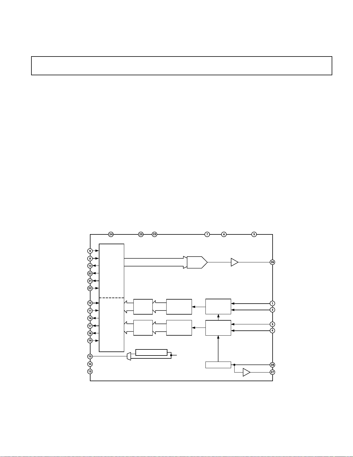
This monolithic 3 V CMOS device is a low power, two-channel,
input port with signal conditioning. The receive path is composed of two high performance sigma-delta ADCs with digital
filtering. A common bandgap reference feeds the ADCs.
A control DAC is included for such functions as AFC. The auxiliary functions can be accessed via the auxiliary port (ASPORT).
This device is available in a 28-lead TSSOP package or a
28-lead SOIC package.
ASDI
ASDIFS
ASCLK
ASDO
ASDOFS
ASE
BSDI
BSDIFS
BSCLK
BSDO
BSDOFS
BSE
MCLK
RxON
RESETB
AUXILIARY
SERIAL
INTERFACE
BASEBAND
SERIAL
INTERFACE
FUNCTIONAL BLOCK DIAGRAM
10-BIT
AUXDAC
DECIMATION
FIR DIGITAL
FILTER
DECIMATION
FIR DIGITAL
FILTER
MUX
OFFSET
ADJUST
OFFSET
ADJUST
DIVIDE BY 2
AVDD1DGNDDVDD1DVDD2 AGND
SD
MODULATOR
SD
MODULATOR
REFERENCE
AVDD2
AUXDAC
IRxP
IRxN
QRxP
QRxN
REFCAP
REFOUT
REV. 0
Information furnished by Analog Devices is believed to be accurate and
reliable. However, no responsibility is assumed by Analog Devices for its
use, nor for any infringements of patents or other rights of third parties
which may result from its use. No license is granted by implication or
otherwise under any patent or patent rights of Analog Devices.
One Technology Way, P.O. Box 9106, Norwood, MA 02062-9106, U.S.A.
Tel: 781/329-4700 World Wide Web Site: http://www.analog.com
Fax: 781/326-8703 © Analog Devices, Inc., 1998

1
AD7729–SPECIFICATIONS
0 V, f
= 13 MHz; RxPOWER1 = 0; RxPOWER0 = 1; MCLKDIV = 0; TA = T
CLK
Parameter AD7729A Units Test Conditions/Comments
REFERENCE
REFCAP
Absolute Voltage, V
REFCAP
REFCAP TC 50 ppm/°C typ 0.1 µF Capacitor Required from REFCAP to AGND
REFOUT
Absolute Voltage, V
REFOUT
REFOUT TC 50 ppm/°C typ 0.1 µF Capacitor Required from REFOUT to AGND
ADC CHANNEL SPECIFICATIONS RxON = 1
Resolution 15 Bits
ADC Signal Range 2 V
V
BIAS
Differential Signal Range V
Single-Ended Signal Range V
Input Sample Rate 13 MSPS
Output Word Rate 270.83 kHz
DC Accuracy
Precalibration Offset Error ±45 mV typ
Post Calibration Offset Error ±10 mV max
Post Calibration Offset Error TC 50 µV/°C typ TC = Temperature Coefficient
Input Resistance (DC) 1.23 MΩ typ
Input Capacitance 10 pF typ
Dynamic Specifications Input Frequency = 67.7 kHz
Dynamic Range 67 dB typ
Signal to (Noise + Distortion) 64 dB min
Gain Error ±1 dB max Input Frequency = 67.7 kHz, wrt 1.3 V
Gain Match Between Channels ±0.2 dB max
Filter Settling Time 47 µs typ
Frequency Response Does Not Include Input Antialias RC Circuit
0 kHz–70 kHz ±0.05 dB max/min
85 kHz –1 dB max
96 kHz –3.0 dB max
135 kHz –55 dB max
>170 kHz –55 dB max
Absolute Group Delay 23 µs typ
Group Delay Between Channels
(0 kHz–96 kHz) 5 ns typ
Coding Twos Complement
AUXILIARY CONVERTER
2
Resolution 10 Bits
Output Range
Code 000 2/32 × V
Offset Error ±35 mV max
Code 3FF 2 V
Gain Error –60 mV min
DC Accuracy Maximum Output for Specified Accuracy = AVDD –
Integral Nonlinearity ±4 LSB max
Differential Nonlinearity ±2 LSB max Guaranteed Monotonic to 9 Bits
Update Rate 540 kHz max
Load Resistance 10 kΩ min See Figure 1
Load Capacitance 50 pF max See Figure 1
I
SINK
Full-Scale Settling Time 4 µs typ
LSB Settling Time 2 µs typ
Coding Binary
1.3 ± 5% V min/max
1.3 ± 10% V min/max
REFCAP
V
/2 to (AVDD – V
REFCAP
V
to (AVDD – V
REFCAP
± V
BIAS
REFCAP
± V
BIAS
REFCAP
±0.5 dB max Input Frequency = 67.7 kHz, wrt V
REFCAP
REFCAP
+100 mV max
50 µA typ
(AVDD1 = AVDD2 = +3 V ⴞ 10%; DVDD1 = DVDD2 = +3 V ⴞ 10%; DGND = AGND =
to T
MIN
/2) Volts Differential
REFCAP
) Volts Single-Ended
REFCAP
/2 V min/max For Both Positive and Negative Analog Inputs
unless otherwise noted)
MAX
V p-p
V min/max For Positive Analog Inputs; Negative Analog Inputs = V
REFCAP
V
V
0.2 V or 2.6 V, Whichever Is Lower
BIAS
–2– REV. 0
AD7729
Parameter AD7729A Units Test Conditions/Comments
LOGIC INPUTS
V
, Input High Voltage VDD – 0.8 V min
INH
V
, Input Low Voltage 0.8 V max
INL
I
, Input Current 10 µA max
IH
CIN, Input Capacitance 10 pF max
LOGIC OUTPUTS
VOH, Output High Voltage VDD – 0.4 V min |I
VOL, Output Low Voltage 0.4 V max |I
I
, Low Level Output Three-State Leakage Current 10 µA max
OZL
I
, High Level Output Three-State Leakage Current 10 µA max
OZH
POWER SUPPLIES
AVDD1, AVDD2 2.7/3.3 V min/max
DVDD1, DVDD2 2.7/3.3 V min/max
I
DD
NOTES
1
Operating Temperature Range: – 40°C to +105°C. Therefore, T
2
During power-down, the AUXDAC has an output resistance of 30 kΩ approximately to AGND.
Specifications subject to change without notice.
= –40°C and T
MIN
= +105°C.
MAX
| < 100 µA
OUT
| < 100 µA
OUT
See Table I
50pF
C
L
R
L
10kV
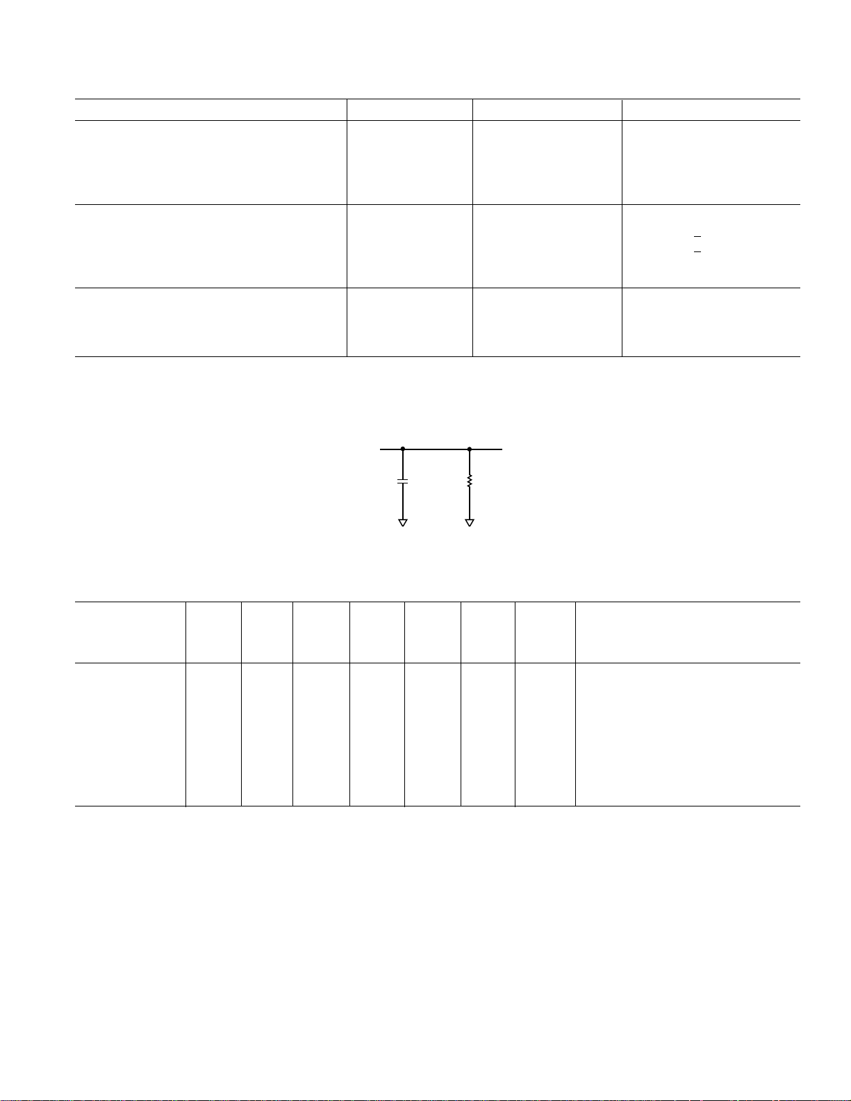
Figure 1. AUXDAC Load Equivalent Circuit
Table I. Current Summary (AVDD1 = AVDD2 = DVDD1 = DVDD2 = +3.3 V, RxPOWER1 = 0, RxPOWER0 = 1)
Internal External
Analog Digital Interface Total
Current Current Current Current MCLK
Conditions (typ) (typ) (typ) (max) BSE ASE ON Comments
ADCs On Only 4.2 3.4 4 13.5 1 0 YES REFOUT Enabled, BSCLK = MCLK
AUXDAC On Only 2 0.86 0.1 3.4 0 1 YES REFOUT Disabled, ASCLK = MCLK/48
REFCAP On Only 0.7 0.0001 0.002 1.1 0 0 NO REFOUT Disabled
REFCAP and
REFOUT On Only 1 0.0001 0.002 1.7 0 0 NO REFOUT Enabled
All Sections Off 0.0001 0.04 0.015 0.1 0 0 YES MCLK Active Levels Equal to 0 V and DVDD
All Sections Off 0.0001 0.0001 0.005 0.05 0 0 NO Digital Inputs Static and Equal to 0 V or
DVDD
The above values are in mA.
–3–REV. 0

AD7729
Table II. Receive Section Signal Ranges
Baseband Section Signal Range
V
REFCAP
V
REFOUT
1.3 V ± 5%
1.3 V ± 10%
ADC
ADC Signal Range 2 V
V
BIAS
Differential Input V
Single-Ended Input V
REFCAP
/2 to (AVDD1 – V
REFCAP
to (AVDD1 – V
REFCAP
REFCAP
REFCAP
AUXDAC Signal Range
Output Code
Code 000 2/32 × V
Code 3FF 2 V
/2)
)
Table III. Auxiliary Section Signal Ranges
REFCAP
REFCAP
Signal Range
Differential V
Single-Ended V
BIAS
BIAS
± V
± V
REFCAP
REFCAP
/2
(AVDD1 = AVDD2 = +3 V ⴞ 10%; DVDD1 = DVDD2 = +3 V ⴞ 10%; AGND = DGND = 0 V;
TIMING CHARACTERISTICS
TA = T
MIN
to T
, unless otherwise noted)
MAX
Limit at
Parameter TA = –40ⴗC to +105ⴗC Units Description
AUXILIARY FUNCTIONS
Clock Signals See Figure 2.
t
1
t
2
t
3
t
4
t
5
t
6
t
10
t
11
t
12
t
13
t
14
t
15
t
16
t
17
76 ns min MCLK Period
30.4 ns min MCLK Width Low
30.4 ns min MCLK Width High
t
1
0.4 × t
0.4 × t
1
1
ns min ASCLK Period. See Figures 4 and 6.
ns min ASCLK Width Low
ns min ASCLK Width High
20 ns min ASDI/ASDIFS Setup Before ASCLK Low
10 ns min ASDI/ASDIFS Hold After ASCLK Low
15 ns max ASDOFS Delay from ASCLK High
0 ns min ASDOFS Hold After ASCLK High
0 ns min ASDO Hold After ASCLK High
15 ns max ASDO Delay from ASCLK High
10 ns min ASDIFS Low to ASDI LSB Read by ASPORT
t4 + 15 ns min Interval Between Consecutive ASDIFS Pulses
Receive Section
Clock Signals See Figures 5 and 7.
t
7
t
8
t
9
t
18
t
19
t
20
t
21
t
22
t
23
t
24
t
25
ASCLK = MCLK/(2 × ASCLKRATE). ASCLKRATE can have a value from 0 . . . 1023. When ASCLKRATE = 0, ASCLK = 13 MHz.
BSCLK = MCLK/(2 × BSCLKRATE). BSCLKRATE can have a value from 0 . . . 1023. When BSCLKRATE = 0, BSCLK = 13 MHz.
Specifications subject to change without notice.
t
1
0.4 × t
0.4 × t
1
1
ns min BSCLK Period
ns min BSCLK Width Low
ns min BSCLK Width High
20 ns min BSDI/BSDIFS Setup Before BSCLK Low
10 ns min BSDI/BSDIFS HoldAfter BSCLK Low
15 ns max BSDOFS Delay from BSCLK High
0 ns min BSDOFS Hold After BSCLK High
0 ns min BSDO Hold After BSCLK High
15 ns max BSDO Delay from BSCLK High
10 ns min BSDIFS Low to ASDI LSB Read by BSPORT
t7 + 15 ns min Interval Between Consecutive BSDIFS Pulses
–4– REV. 0
TIMING DIAGRAMS
t
6
t
4
t
1
t
3
t
2
t
5
MCLK
*ASCLK
*ASCLK IS INDIVIDUALLY PROGRAMMABLE IN FREQUENCY
(MCLK/4 SHOWN HERE).
t
9
t
7
t
1
t
3
t
2
t
8
MCLK
*BSCLK
*BSCLK IS INDIVIDUALLY PROGRAMMABLE IN FREQUENCY
(MCLK/4 SHOWN HERE).
t
3
AD7729
t
1
t
2
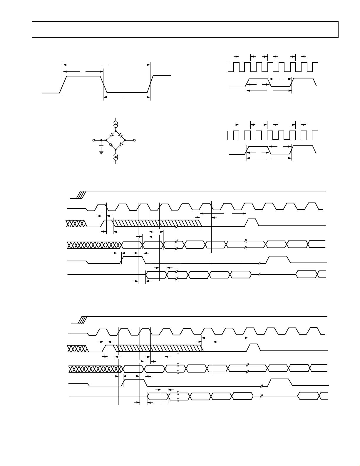
Figure 2. Clock Timing
TO OUTPUT PIN
15pF
C
L
100mAI
100mA
OL
+2.1V
I
OH
Figure 3. Load Circuit for Timing Specifications
ASE (I)
ASCLK (O)
ASDIFS (I)
ASDOFS (O)
ASDO (O)
THREE-STATE
ASDI (I)
THREE-STATE
THREE-STATE
NOTE
I = INPUT, O = OUTPUT
t
10
t
11
D9 D8
t
12
t
11
t
10
t
13
D9
t
15
Figure 4. ASCLK
Figure 5. BSCLK
t
t
16
A1 A0
t
14
A2
17
D9 D8
A1
A0
D7
D8D9
BSE (I)
BSCLK (O)
BSDIFS (I)
BSDOFS (O)
BSDO (O)
THREE-STATE
BSDI (I)
THREE-STATE
THREE-STATE
NOTE
I = INPUT, O = OUTPUT
Figure 6. Auxiliary Serial Port ASPORT
t
18
t
t
19
D9 D8
t
20
t
19
t
18
A1 A0 D9 D8 D7
t
21
t
22
D9
t
23
A2
t
24
25
A1
D8D9A0
Figure 7. Baseband Serial Port BSPORT
–5–REV. 0
 Loading...