16-Bit 900 kSPS - ADC with a
2.5V
REFERENCE
POST-
PROCESSOR
DEFAULT FILTER
(ROM )
XTAL
CLOCK
PRESET
FILTER
MOD
CONTROL
LOGIC
UNI
HALF
PWR
STBY
SYNC
S/P
V
IN
(+)
V
IN
(–)
RD/ WR
SOE/ CS
CFMT/RS
DVAL/ INT
SDI/DB0
ERR/ DB1
DB2
DB3
RESETCFG/DB4
INT/DB5
FSI/ DB6
SCO/ DB7
SDO/ DB8
SCR/ DB13
CFGEND/DB12
DB11
DB10
FSO/DB9
SMODE1/ DB15
SMODE0/ DB14
XTAL_OFF
XTAL
CLKIN
DV
DD
DGND
REF2
REF1
AV
DD
AGND
AD7725
Programmable Postprocessor
AD7725
FEATURES
Programmable Filtering:
Any Characteristic up to 108 Tap FIR and/or IIR
Polynomial Signal Conditioning up to 8
th
Order
Programmable Decimation and Output Word Rate
Flexible Programming Modes:
Boot from DSP or External EPROM
Parallel/Serial Interface
Internal Default Filter for Evaluation
14.4 MHz Max Master Clock Frequency
0 V to +4 V (Single-Ended) or 2 V (Differential) Input
Range
Power Supplies: AVDD, DVDD: 5 V 5%
On-Chip 2.5 V Voltage Reference
44-Lead MQFP Package
TYPICAL APPLICATIONS
Radar
Sonar
Auxiliary Car Functions
Medical Communications
GENERAL DESCRIPTION
The AD7725 is a complete 16-bit, - analog-to-digital converter with on-chip, user-programmable signal conditioning. The
output of the modulator is processed by three cascaded finite
impulse response (FIR) filters, followed by a fully user-programmable postprocessor. The postprocessor provides processing
power of up to 130 million accumulates (MAC) per second. The
user has complete control over the filter response, the filter coefficients, and the decimation ratio.
The postprocessor permits the signal conditioning characteristics
to be programmed through a parallel or serial interface.
is programmed by loading a user-defined filter in the form of a
configuration file. This filter can be loaded from a DSP or an
external serial EPROM. It is generated using a digital filter
design package called Filter Wizard, which is available from the
AD7725 section on the Analog
Devices
website.
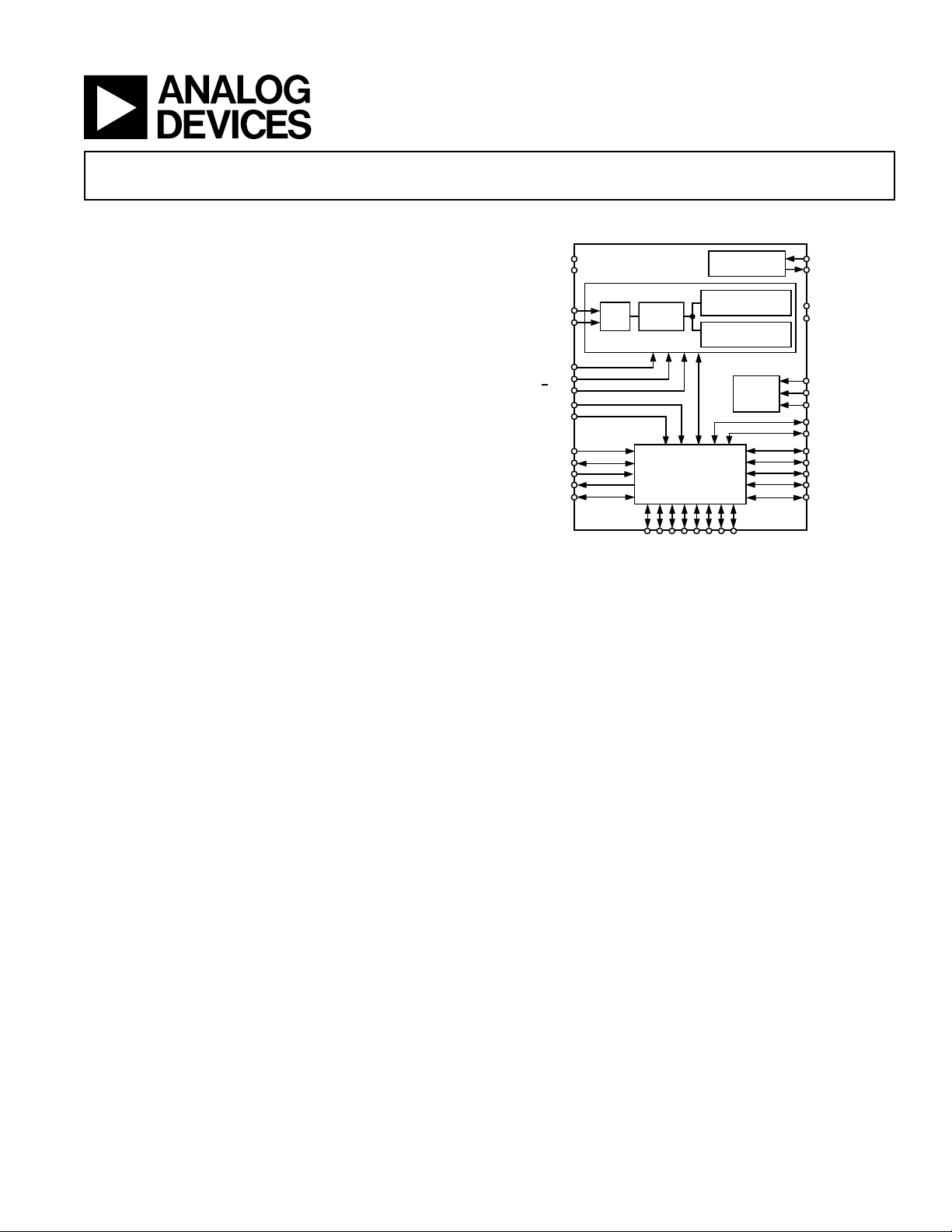
FUNCTIONAL BLOCK DIAGRAM
t
Filter Wizard allows the user
and generates the appropriate
loaded to the postprocessor. The
o design different filter types
configuration file to be down-
AD7725 also has an internal
default filter for evaluation purposes.
It provides 16-bit performance for input bandwidths up to
350 kHz with an output word rate of 900 kHz maximum. The
input sample rate is set either by the crystal oscillator or an
external clock.
This part has an accurate on-chip 2.5 V reference for the modu-
It
lator. A reference input/output function allows either the
internal reference or an external system reference to be used as
the reference source for the modulator.
The device is available in a 44-lead MQFP package and is specified over a –40°C to +85°C temperature range.
REV. A
Information furnished by Analog Devices is believed to be accurate and
reliable. However, no responsibility is assumed by Analog Devices for its
use, nor for any infringements of patents or other rights of third parties that
may result from its use. No license is granted by implication or otherwise
under any patent or patent rights of Analog Devices. Trademarks and
registered trademarks are the property of their respective owners.
One Technology Way, P.O. Box 9106, Norwood, MA 02062-9106, U.S.A.
Tel: 781/329-4700 www.analog.com
Fax: 781/326-8703 © 2004 Analog Devices, Inc. All rights reserved.

(AVDD = 5 V 5%, AGND = AGND1 = AGND2 = DGND = 0 V,
1
AD7725–SPECIFICATIONS
2
f
= 9.6 MHz, REF2 = 2.5 V, TA = T
CLKIN
MIN
to T
, unless otherwise noted.)
MAX
B Version
Parameter Test Conditions/Comments Min Typ Max Unit
DYNAMIC SPECIFICATIONS When tested with the FIR filter in
Figure 1, HALF_PWR = Logic High
Bipolar Mode
Signal-to-Noise
3
Measurement Bandwidth = 0.5 f
4
O
2.5 V Reference 77 83 dB
3 V Reference 79 85 dB
3, 5
Measurement Bandwidth = 0.5 f
4
O
–94 –86 dB
–98 –89 dB
83 dB
–94 dB
Total Harmonic Distortion
Spurious Free Dynamic Range
Unipolar Mode
Signal-to-Noise
3
Total Harmonic Distortion
3, 5
3, 5
ANALOG INPUTS
Full-Scale Input Span V
Bipolar Mode Differential or Single-Ended Input ±4/5 V
Unipolar Mode Single-Ended Input 0 8/5 V
Absolute Input Voltage V
Input Sampling Capacitance 2 pF
Input Sampling Rate, f
CLKIN
(+) – VIN(–)
IN
(+) and/or VIN(–) AGND AV
IN
14.4
DD
V
REF2
REF2
V
V
6
MHz
CLOCK
CLKIN Duty Ratio 45 55 %
REFERENCE
REF1 Output Resistance 3.5 kΩ
Reference Buffer
Offset Voltage Offset between REF1 and REF2 ±3mV
Using Internal Reference
REF2 Output Voltage 2.39 2.54 2.69 V
REF2 Output Voltage Drift 60 ppm/°C
Using External Reference
REF2 Input Impedance REF1 = AGND 8 kΩ
REF2 External Voltage Input
7
2.5 V
STATIC PERFORMANCE
Resolution 16 Bits
Differential Nonlinearity (DNL)
Integral Nonlinearity (INL)
3
3
Guaranteed Monotonic ±0.5 ±1
±2 LSB
8
LSB
DC CMRR 80 dB
Offset Error ±20 mV
Gain Error
3, 9
±0.5 %FSR
LOGIC INPUTS (Excluding CLKIN)
V
, Input High Voltage 2.0 V
INH
V
, Input Low Voltage 0.8 V
INL
CLOCK INPUT (CLKIN)
V
, Input High Voltage 0.7 DV
INH
V
, Input Low Voltage 0.3 DV
INL
DD
DD
V
V
REV. A–2–
AD7725
B Version
Parameter Test Conditions/Comments Min Typ Max Unit
ALL LOGIC INPUTS
IIN, Input Current VIN = 0 V to DV
DD
CIN, Input Capacitance 10 pF
LOGIC OUTPUTS
, Output High Voltage |I
V
OH
VOL, Output Low Voltage |I
POWER SUPPLIES
AV
DD
11
AI
DD
DV
DD
13
DI
DD
Power Consumption
NOTES
1
Operating temperature range is as follows: B Version: –40°C to +85°C.
2
f
is the CLKIN frequency.
CLKIN
3
See Terminology section.
4
FO = output data rate.
5
When using the internal reference, THD and SFDR specifications apply only to input signals above 10 kHz with a 10 µF decoupling capacitor between REF2 and
AGND2. At frequencies below 10 kHz, THD degrades to –80 dB and SFDR degrades to –83 dB.
6
See Figures 23 and 24 for information regarding the number of filter taps allowed and the current consumption as the CLKIN frequency is varied.
7
The AD7725 can operate with an external reference input in the range of 1.2 V to 3.15 V.
8
Guaranteed by the design.
9
Gain Error excludes reference error.
10
All IDD tests are done with the digital inputs equal to 0 V or DVDD.
11
Analog current does not vary as the CLKIN frequency and the number of filter taps used in the postprocessor is varied.
12
If HALF_PWR is logic low, AIDD will typically double.
13
Digital current varies as the CLKIN frequency and the number of filter taps used in the postprocessor is varied. See Figures 23 and 24.
14
Digital inputs static and equal to 0 V or DVDD.
Specifications subject to change without notice.
10
14
| = 200 µA 4.0 V
OUT
| = 1.6 mA 0.4 V
OUT
HALF_PWR = Logic High
12
4.75 5.25 V
28 33 mA
4.75 5.25 V
With the Filter in Figure 1 84 90 mA
Standby Mode 30 mW
±10 µA
0
–20
–40
–60
–80
ATTENUATION – dB
–100
–120
–140
0 30050
CUTOFF FREQUENCY = 50kHz
STOP-BAND FREQUENCY = 116kHz
NUMBER OF FILTER TAPS USED IN
THE POSTPROCESSOR = 108
OUPUT DATA RATE = CLKIN/16
100 150 200 250
116
FREQUENCY – kHz
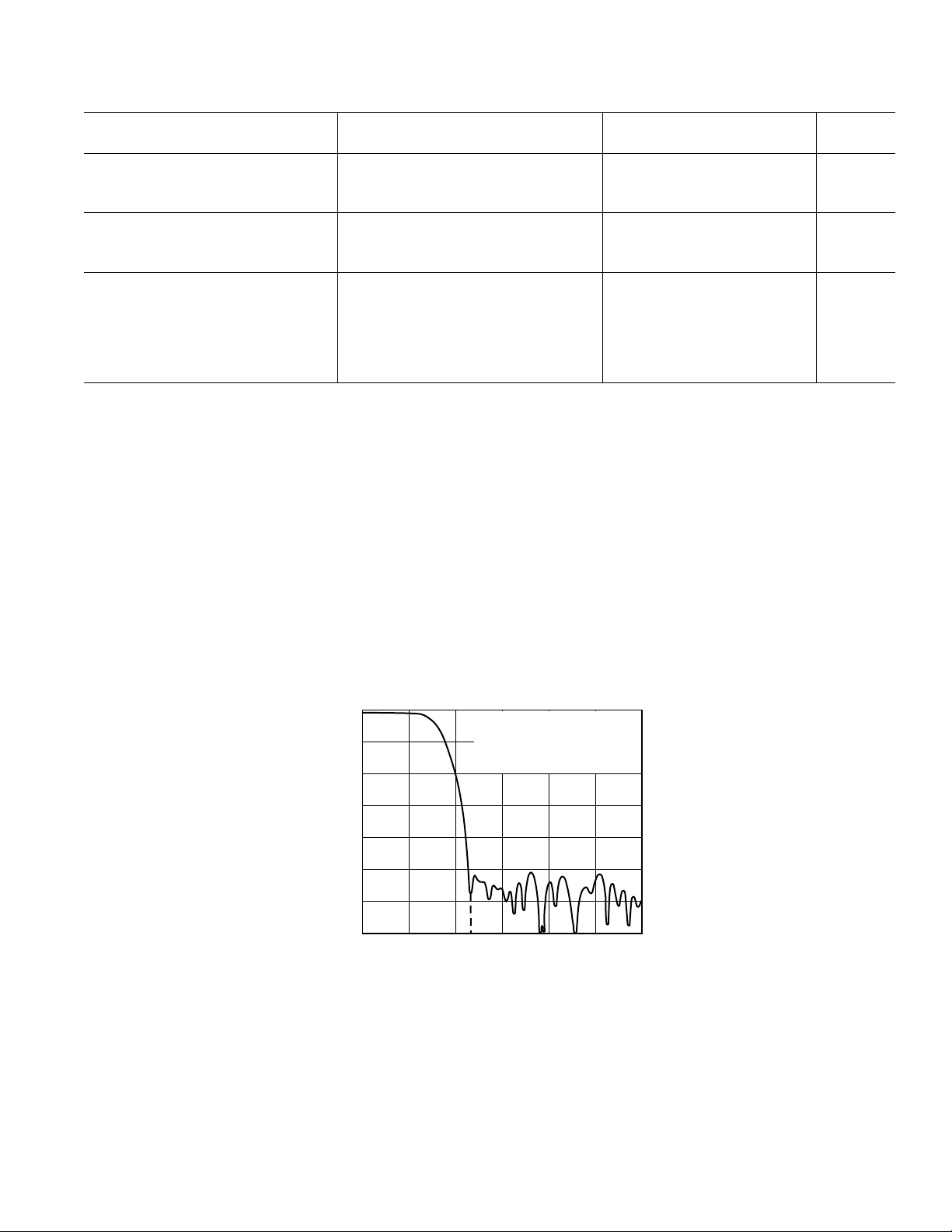
Figure 1. Digital Filter Characteristics Used for Specifications
REV. A
–3–

AD7725
Preset Filter, Default Filter, and Postprocessor Characteristics
1, 2
Parameter Test Conditions/Comments Min Typ Max Unit
DIGITAL FILTER RESPONSE
PRESET FIR
Data Output Rate f
/8 Hz
CLKIN
Stop-Band Attenuation 70 dB
Low-Pass Corner Frequency f
Group Delay
Settling Time
3
3
/16 Hz
CLKIN
133/(2 f
133/f
CLKIN
)s
CLKIN
s
DEFAULT FILTER Internal FIR Filter Stored in ROM
Number of Taps 106
Frequency Response
0 kHz to f
/195.04 –3 dB
f
CLKIN
f
/184.08 –6 dB
CLKIN
/133.2 to f
f
CLKIN
Group Delay
Settling Time
Output Data Rate, f
/546.08 ± 0.001 dB
CLKIN
/2 –120 dB
CLKIN
3
3
O
2141/(2 f
2141/f
CLKIN
f
/32 Hz
CLKIN
)s
CLKIN
s
POSTPROCESSOR CHARACTERISTICS
Input Data Rate f
Coefficient Precision
4
24 Bits
/8 Hz
CLKIN
Arithmetic Precision 30 Bits
Number of Taps Permitted 108
Decimation Factor 2 256
Number of Decimation Stages 1 5
Output Data Rate f
NOTES
1
These characteristics are fixed by the design.
2
f
is the CLKIN frequency.
CLKIN
3
See Terminology section.
4
See the Configuration File Format section for more information.
/4096 f
CLKIN
/16 Hz
CLKIN
REV. A–4–

TIMING SPECIFICATIONS
(AVDD = 5 V 5%; DVDD = 5 V 5%; AGND = DGND = 0 V, REF2 = 2.5 V,
unless otherwise noted.)
AD7725
1, 2
Parameter Symbol Min Typ Max Unit
CLKIN Frequency f
CLKIN Period (t
CLK
= 1/f
)t
CLKIN
CLKIN Low Pulse Width t
CLKIN High Pulse Width t
CLKIN Rise Time t
CLKIN Fall Time t
CLKIN to SCO Delay t
SCO Period: SCR = 0 t
SCR = 1 t
CLKIN
1
2
3
4
5
6
7
7
114.4MHz
0.07 1 µs
0.45 t
0.45 t
1
1
0.55 t
0.55 t
1
1
5ns
5ns
35 50 ns
1t
2t
SERIAL INTERFACE (DSP MODE ONLY)
FSI Setup Time before SCO Transition t
FSI Hold Time after SCO Transition t
SDI Setup Time t
SDI Hold Time t
8
9
10
11
30 ns
0ns
30 ns
0ns
SERIAL INTERFACE (DSP AND BFR MODES)
SCO Transition to FSO High Delay t
SCO Transition to FSO Low Delay t
SDO Setup before SCO Transition t
SDO Hold after SCO Transition t
12
13
14
15
0ns
20 ns
20 ns
10 ns
SERIAL INTERFACE (EPROM MODE)
SCO High Time t
SCO Low Time t
SOE Low to First SCO Rising Edge t
Data Setup before SCO Rising Edge t
16
17
18
19
22 ns
8t
8t
20 t
PARALLEL INTERFACE
DATA WRITE
RS Low to CS Low t
WR Setup before CS Low t
RS Hold after CS Rising Edge t
CS Pulse Width t
WR Hold after CS Rising Edge t
Data Setup Time t
Data Hold Time t
20
21
22
23
24
25
26
15 ns
15 ns
0ns
50 ns
0ns
10 ns
5ns
DATA READ
RS Low to CS Low t
RD Setup before CS Low t
RS Hold after CS Rising Edge t
RD Hold after CS Rising Edge t
Data Valid after CS Falling Edge
3
Data Hold after CS Rising Edge t
27
28
29
30
t
31
32
15 ns
15 ns
0ns
0ns
30 ns
10 ns
STATUS READ/INSTRUCTION WRITE
CS Duty Cycle t
Interrupt Clear after CS Low t
RD Setup to CS Low t
RD Hold after CS Rising Edge t
Read Data Access Time
3
Read Data Hold after CS Rising Edge t
Write Data Setup before CS Rising Edge t
Write Data Hold after CS Rising Edge t
NOTES
1
Guaranteed by design.
2
Guaranteed by characterization. All input signals are specified with tr tf 5 ns (10% to 90% of DVDD) and timed from a voltage level of 1.6 V.
3
Measured with the load circuit in Figure 2 and defined as the time required for the output to cross 0.8 V and 2.4 V.
33
34
35
36
t
37
38
39
40
1t
15 ns
15 ns
0ns
30 ns
10 ns
10 ns
5ns
CLK
CLK
CLK
CLK
CLK
CLK
REV. A
–5–
AD7725
I
OL
1.6mA
TO
OUTPUT
PIN
25pF
C
L
I
OH
200A
1.6V
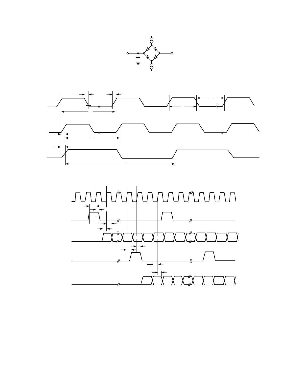
Figure 2. Load Circuit for Digital Output Timing Specifications
CLKIN
SCO
SCR = 0
SCO
SCR = 1
2.3V
CFMT = 0
SCO
FSI
SDI
t
5
0.8V
t
1
t
6
t
6
t
7
t
4
t
3
t
7
t
2
Figure 3. CLKIN to SCO Relationship
t
8
t
9
t
t
10
11
D15 D0 D15 D4 D3 D2 D1
D4 D2D3 D1
t
13
t
14
t
15
D15 D14 D13 D12 D1 D0 D15 D14
FSO
SDO
t
12
Figure 4. Serial Mode (DSP Mode and Boot from ROM (BFR) Mode). In BFR Mode, FSI and SDI are not used.
REV. A–6–
S
INT
RD/WR
RS
CS
t
16
SCO
t
17
t
19
CO
SDI
t
18
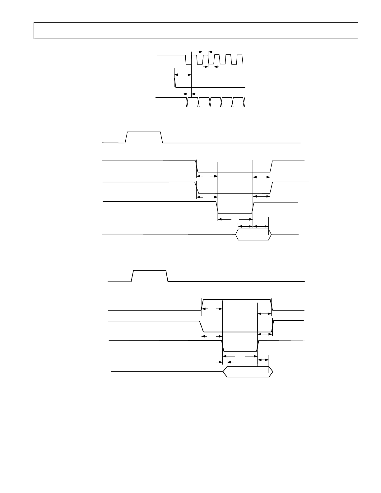
Figure 5. Serial Mode (EPROM Mode)
t
21
t
20
AD7725
t
24
t
22
DB0 DB15
–
RD/WR
DB0 DB15
–
INT
RS
CS
t
23
THREE-STATE
t
t
26
25
VALID DATA
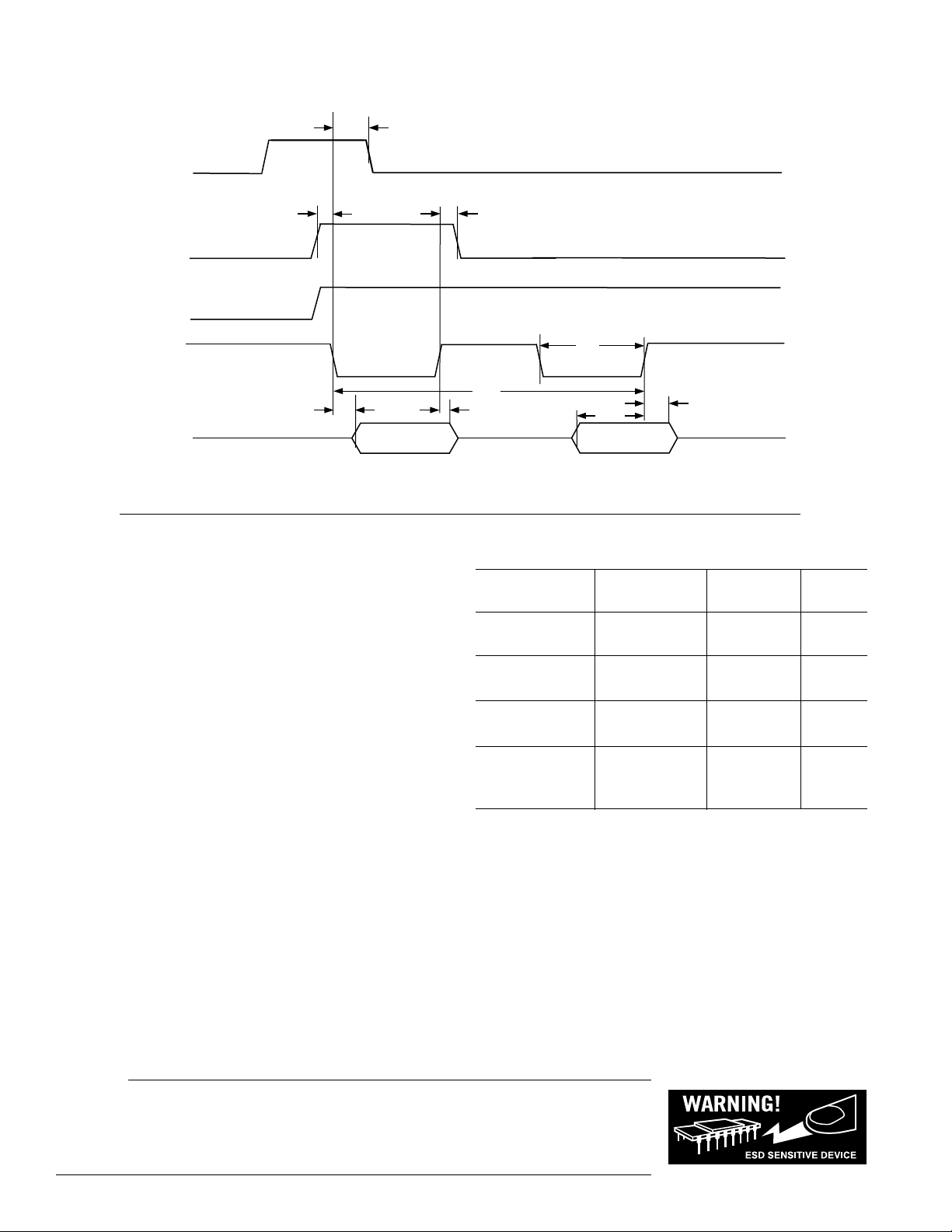
Figure 6. Parallel Mode (Writing Data to the AD7725)
t
THREE-STATE
28
t
27
t
t
31
23
VA LID DATA
t
30
t
29
t
32
Figure 7. Parallel Mode (Reading Data from the AD7725)
THREE-STATE
THREE-STATE
REV. A
–7–
AD7725
INT
t
34
RD/WR
RS
CS
DB0 DB15
–
t
35
t
37
STATU
THREE-STATE THREE-STATE THREE-STATE
S
t
36
t
23
t
33
t
38
t
39
INSTRUCTI
ON
Figure 8. Parallel Mode (Reading the Status Register and Writing Instructions)
ABSOLUTE MAXIMUM RATINGS
(TA = 25°C, unless otherwise noted.)
to DGND . . . . . . . . . . . . . . . . . . . . . . . . –0.3 V to +7 V
DV
DD
to AGND . . . . . . . . . . . . . . . . . . . . . . . . . –0.3 V to +7 V
AV
DD
AV
DD
, AV
to DVDD . . . . . . . . . . . . . . . . . . . . –1 V to +1 V
DD1
1
ORDERING GUIDE
Temperature Package Package
Model Range Description Option
AD7725BS –40°C to +85°CMetric Quad S-44-2
AGND, AGND1 to DGND . . . . . . . . . . . . . –0.3 V to +0.3 V
Digital Inputs to DGND . . . . . . . . . . –0.3 V to DV
Digital Outputs to DGND . . . . . . . . . –0.3 V to DV
V
(+), VIN(–) to AGND . . . . . . . . . . . –0.3 V to AVDD + 0.3 V
IN
REF1 to AGND . . . . . . . . . . . . . . . . . –0.3 V to AV
REF2 to AGND . . . . . . . . . . . . . . . . . –0.3 V to AV
REFIN to AGND . . . . . . . . . . . . . . . . –0.3 V to AV
DGND, AGND . . . . . . . . . . . . . . . . . . . . . . . . . . . . . . . ± 0.3 V
Input Current to Any Pin except Supplies
I
(AI
DD
+ DIDD) . . . . . . . . . . . . . . . . . . . . . . . . . . . . 150 mA
DD
2
. . . . . . . . . ± 10 mA
Operating Temperature Range . . . . . . . . . . . .–40°C to +85°C
Storage Temperature Range . . . . . . . . . . . . . –65°C to +150°C
Junction Temperature . . . . . . . . . . . . . . . . . . . . . . . . . . 150°C
Thermal Impedance . . . . . . . . . . . . . . . . . . . . . . . . 58°C/W
JA
Thermal Impedance . . . . . . . . . . . . . . . . . . . . . . . . 20°C/W
JC
Lead Temperature, Soldering
Vapor Phase (60 sec) . . . . . . . . . . . . . . . . . . . . . . . . . 215°C
Infrared (15 sec) . . . . . . . . . . . . . . . . . . . . . . . . . . . . 220°C
ESD . . . . . . . . . . . . . . . . . . . . . . . . . . . . . . . . . . . . . . . . . . 2 kV
NOTES
1
Stresses above those listed under Absolute Maximum Ratings may cause permanent damage to the device. This is a stress rating only; functional operation of the
device at these or any other conditions above those indicated in the operational
section of this specification is not implied. Exposure to absolute maximum rating
conditions for extended periods may affect device reliability.
2
Transient currents of up to 100 mA will not cause SCR latch-up.
+ 0.3 V
DD
+ 0.3 V
DD
+ 0.3 V
DD
+ 0.3 V
DD
+ 0.3 V
DD
AD7725BS-REEL –40°C to +85°CMetric Quad S-44-2
EVAL- Evaluation
AD7725CB
2
EVAL- Controller
CONTROL Board
3
BRD2
NOTES
1
S = Metric Quad Flat Package (MQFP).
2
This board can be used as a standalone evaluation board or in conjunction with the
Evaluation Board Controller for evaluation/demonstration purposes. It is accompanied by software and technical documentation.
3
Evaluation Board Controller. This board is a complete unit allowing a PC to
control and communicate with all Analog Devices boards ending in the CB
designator. To obtain the complete evaluation kit, the following needs to be
ordered: EVAL-AD7725CB, EVAL-CONTROL BRD2, and a 12 V ac transformer.
The Filter Wizard software can be downloaded from the Analog Devices website.
CAUTION
ESD (electrostatic discharge) sensitive device. Electrostatic charges as high as 4000 V readily
accumulate on the human body and test equipment and can discharge without detection. Although the
AD7725 features proprietary ESD protection circuitry, permanent damage may occur on devices
subjected to high energy electrostatic discharges. Therefore, proper ESD precautions are recommended
to avoid performance degradation or loss of functionality.
t
40
1
Flatpack
Flatpack
Board
REV. A–8–

EFMT/DB2
ERR/DB1
SDI/DB0
CFMT/RS
DVAL/INT
DGND
RD/WR
S/P
AGND1
AGND1
AV
DD1
PIN CONFIGURATION
DD
RESETCFG/DB4
DGND/DB3
1
PIN 1
IDENTIFIER
2
3
4
5
6
7
8
9
10
11
12 13 14 15 1 6 17 18 19 20 21 2 2
CLKIN
FSI/DB6
INIT/DB5
(Not to Scale)
XTAL
XTALOFF
HALF_PWR
SDO/DB8
DV
SCO/DB7
40 39 3841424344 36 35 3437
AD7725
TOP VIEW
DD
AGND
AV
AGND
DGND/DB10
FSO/DB9
)
)
–
+
(
(
IN
IN
V
V
CFGEND/DB12
DGND/DB11
33
32
31
30
29
28
27
26
25
24
23
REF1
AGND2
SCR/DB13
SMODE0/DB14
SMODE1/DB15
SOE/CS
SYNC
DGND
STBY
AV
DD
AGND
UNI
REF2
AD7725
PIN FUNCTION DESCRIPTIONS
Pin No. Mnemonic S/P Description
1 EFMT/DB2 Serial Mode. EFMT–Serial Clock Format, Logic Input. This clock format pin selects
the clock edge to be used during configuration. When EFMT is low, Serial Data In is
valid on the rising edge of SCO; when EFMT is high, Serial Data In is valid
on the falling edge of SCO. During normal operation, this pin is ignored.
Parallel Mode. DB2–Data Input/Output Bit.
2 ERR/DB1 Serial Mode. ERR–Configuration Error Flag, Logic Output. If an error occurs during
configuration, this output goes low and is reset high by a pulse on the RESETCFG pin.
Parallel Mode. DB1–Data Input/Output Bit.
3 SDI/DB0 Serial Mode. SDI–Serial Data Input. Serial data is shifted in to the AD7725 MSB first, in
twos complement format, synchronous with SCO.
Parallel Mode. DB0–Data Input/Output Bit (LSB).
4 CFMT/RS Serial Mode. CFMT–Serial Clock Format, Logic Input. This clock format pin selects the
clock edge to be used during normal operation. When CFMT is low, Serial Data Out is
valid on the rising edge of SCO; when CFMT is high, Serial Data Out is valid on the
falling edge of SCO. During configuration, this pin is ignored.
Parallel Mode. RS–Register Select. RS selects between the data register, used to read
conversion data or write configuration data, and the instruction register. When RS is high,
the status register can be read or an instruction can be written to the AD7725. When RS
is low, data such as the configuration file can be written to the ADC while data such as the
device ID or a conversion result can be read from the AD7725 (see Table I).
REV. A
–9–
 Loading...