

Analog Devices AD7723BS Datasheet
16-Bit, 1.2 MSPS
a
FEATURES
16-Bit Sigma-Delta ADC
1.2 MSPS Output Word Rate
32/16 3 Oversampling Ratio
Low-Pass and Band-Pass Digital Filter
Linear Phase
On-Chip 2.5 V Voltage Reference
Standby Mode
Flexible Parallel or Serial Interface
Crystal Oscillator
Single +5 V Supply
AV
AGND
VIN(+)
VIN(–)
UNI
HALF_PWR
STBY
MODE 1
MODE 2
SYNC
DVDD/CS
CFMT/RD
DGND/DRDY
DGND/DB0
CMOS, Sigma-Delta ADC
AD7723
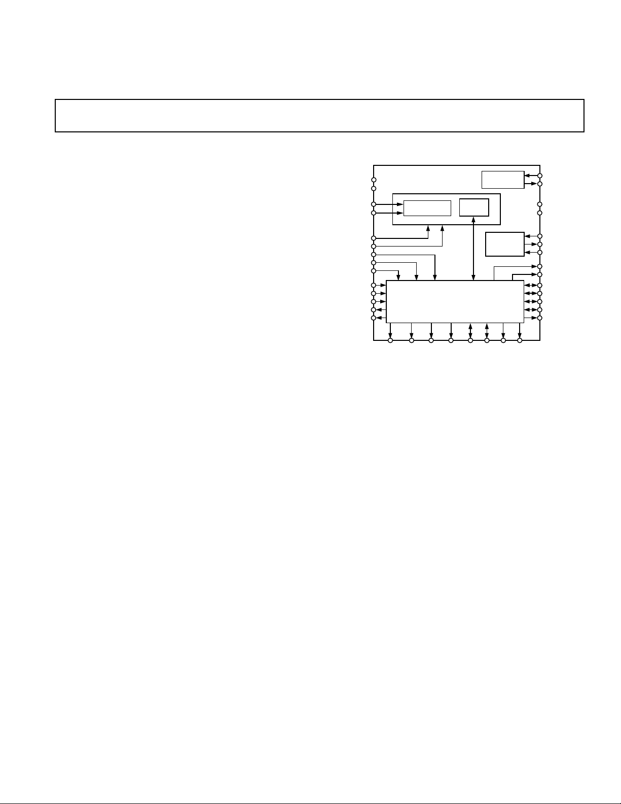
FUNCTIONAL BLOCK DIAGRAM
FIR
FSI/
DB6
2.5V
REFERENCE
XTAL
CLOCK
SCO/
DB7
SDO/
DB8
DD
DGND/
DB1
AD7723
MODULATOR
DGND/
DGND/
DB2
DB3
CONTROL
LOGIC
DOE/
SFMT/
DB4
FILTER
DB5
REF2
REF1
DV
DD
DGND
XTAL_OFF
XTAL
CLKIN
DGND/DB15
DGND/DB14
SCR/DB13
SLDR/DB12
SLP/DB11
TSI/DB10
FSO/DB9
GENERAL DESCRIPTION
The AD7723 is a complete 16-bit, sigma-delta ADC. The part
operates from a +5␣ V supply. The analog input is continuously
sampled, eliminating the need for an external sample-and-hold.
The modulator output is processed by a finite impulse response
(FIR) digital filter. The on-chip filtering combined with a high
oversampling ratio reduces the external antialias requirements
to first order in most cases. The digital filter frequency response
can be programmed to be either low pass or band pass.
The AD7723 provides 16-bit performance for input bandwidths
up to 460␣ kHz at an output word rate up to 1.2 MHz. The
sample rate, filter corner frequencies and output word rate are
set by the crystal oscillator or external clock frequency.
Data can be read from the device in either serial or parallel
format. A stereo mode allows data from two devices to share a
single serial data line. All interface modes offer easy, high speed
connections to modern digital signal processors.
The part provides an on-chip 2.5␣ V reference. Alternatively, an
external reference can be used.
A power-down mode reduces the idle power consumption to
200 µW.
The AD7723 is available in a 44-lead PQFP package and is
specified over the industrial temperature range from –40°C to
+85°C.
Two input modes are provided, allowing both unipolar and
bipolar input ranges.
REV. 0
Information furnished by Analog Devices is believed to be accurate and
reliable. However, no responsibility is assumed by Analog Devices for its
use, nor for any infringements of patents or other rights of third parties
which may result from its use. No license is granted by implication or
otherwise under any patent or patent rights of Analog Devices.
One Technology Way, P.O. Box 9106, Norwood, MA 02062-9106, U.S.A.
Tel: 781/329-4700 World Wide Web Site: http://www.analog.com
Fax: 781/326-8703 © Analog Devices, Inc., 1998

(AVDD = DVDD = +5 V 6 5%; AGND = AGND1 = AGND2 = DGND = 0 V;
1
f
AD7723–SPECIFICATIONS
= 19.2 MHz; REF2 = 2.5 V; TA = T
CLKIN
MIN
to T
; unless otherwise noted)
MAX
B Version
Parameter Test Conditions/Comments Min Typ Max Units
DYNAMIC SPECIFICATIONS
Decimate by 32
Bipolar Mode
Signal to Noise
Full Power 2.5 V Reference 87 90 dB
Half Power 86.5 89 dB
Total Harmonic Distortion
Spurious Free Dynamic Range
Unipolar Mode
Signal to Noise 87 dB
Total Harmonic Distortion
Spurious Free Dynamic Range
Bandpass Filter Mode
Bipolar Mode
Signal to Noise 76 79 dB
Decimate by 16
Bipolar Mode
Signal to Noise Measurement Bandwidth = 0.383 × F
Signal to Noise Measurement Bandwidth = 0.5 × F
Total Harmonic Distortion
Spurious Free Dynamic Range
Unipolar Mode
Signal to Noise Measurement Bandwidth = 0.383 × F
Signal to Noise Measurement Bandwidth = 0.5 × F
Total Harmonic Distortion
DIGITAL FILTER RESPONSE
Low Pass Decimate by 32
0 kHz to f
f
/66.9 –3 dB
CLKIN
f
/64 –6 dB
CLKIN
f
/51.9 to f
CLKIN
/83.5 ±0.001 dB
CLKIN
CLKIN
Group Delay 1293/2f
Settling Time 1293/f
Low Pass Decimate by 16
0 kHz to f
f
/33.45 –3 dB
CLKIN
f
/32 –6 dB
CLKIN
f
/25.95 to f
CLKIN
/41.75 ±0.001 dB
CLKIN
CLKIN
Group Delay 541/2f
Settling Time 541/f
Band Pass Decimate by 32
f
/51.90 to f
CLKIN
f
/62.95, f
CLKIN
f
/64, f
CLKIN
0 kHz to f
CLKIN
CLKIN
/32 –6 dB
CLKIN
/83.5, f
CLKIN
Group Delay 1293/2f
Settling Time 1293/f
Output Data Rate, F
O
Decimate by 32 f
Decimate by 16 f
ANALOG INPUTS
Full-Scale Input Span VIN(+) – VIN(–)
Bipolar Mode ±4/5 × V
Unipolar Mode 0 8/5 × V
2, 3
HALF_PWR = 0 or 1
f
= 10 MHz When HALF-PWR = 1
CLKIN
3 V Reference 88.5 91 dB
4
4
2.5 V Reference –92 dB
–96 –90 dB
3 V Reference –90 dB
4
4
O
–89 dB
–90 dB
2.5 V Reference 82 86 dB
3 V Reference 83 87 dB
4
2.5 V Reference –88 dB
3 V Reference –86 dB
4
2.5 V Reference –90 dB
O
78 81.5 dB
3 V Reference –88 dB
O
4
O
84 dB
81 dB
–89 dB
/2 –90 dB
CLKIN
CLKIN
/2 –90 dB
CLKIN
CLKIN
/41.75 ±0.001 dB
/33.34 –3 dB
CLKIN
/25.95 to f
/2 –90 dB
CLKIN
CLKIN
CLKIN
/32
CLKIN
/16
CLKIN
REF2
REF2
V
V
–2– REV. 0

AD7723
B Version
Parameter Test Conditions/Comments Min Typ Max Units
ANALOG INPUTS (Continued)
Absolute Input Voltage VIN(+) and/or VIN(–) AGND AV
DD
Input Sampling Capacitance 2pF
Input Sampling Rate, f
CLKIN
19.2 MHz
CLOCK
CLKIN Duty Ratio 45 55 %
REFERENCE
REF1 Output Resistance 3kΩ
Using Internal Reference
REF2 Output Voltage 2.39 2.54 2.69 V
REF2 Output Voltage Drift 60 ppm/°C
Using External Reference
REF2 Input Impedance REF1 = AGND 4 kΩ
REF2 External Voltage Range 1.2 2.5 3.15 V
STATIC PERFORMANCE
Resolution 16 Bits
Differential Nonlinearity Guaranteed Monotonic ±0.5 ±1 LSB
Integral Nonlinearity ±2 LSB
DC CMRR 80 dB
Offset Error ±20 mV
Gain Error
5
±0.5 % FSR
LOGIC INPUTS (Excluding CLKIN)
, Input High Voltage 2.0 V
V
INH
V
, Input Low Voltage 0.8 V
INL
CLOCK INPUT (CLKIN)
V
, Input High Voltage 3.8 V
INH
V
, Input Low Voltage 0.4 V
INL
ALL LOGIC INPUTS
I
, Input Current VIN = 0 V to DV
IN
DD
±10 µA
CIN, Input Capacitance 10 pF
LOGIC OUTPUTS
, Output High Voltage |I
V
OH
VOL, Output Low Voltage |I
| = 200 µA 4.0 V
OUT
| = 1.6 mA 0.4 V
OUT
POWER SUPPLIES
AV
I
AVDD
DD
HALF_PWR = Logic Low 50 60 mA
4.75 5.25 V
HALF_PWR = Logic High 25 33 mA
DV
DD
I
DVDD
Power Consumption
NOTES
1
Operating temperature range is as follows: B Version: –40°C to +85°C.
2
Typical values for SNR apply for parts soldered directly to a printed circuit board ground plane.
3
Dynamic specifications apply for input signal frequencies from dc to 0.0240 × f
4
When using the internal reference, THD and SFDR specifications apply only to input signals above 10 kHz with a 10 µF decoupling capacitor between REF2 and
AGND2. At frequencies below 10 kHz, THD degrades to 84 dB and SFDR degrades to 86 dB.
5
Gain Error excludes Reference Error.
6
CLKIN and digital inputs static and equal to 0 or DVDD.
Specifications subject to change without notice.
6
HALF_PWR = Logic Low 25 35 mA
HALF_PWR = Logic High 15 20 mA
Standby Mode 200 µW
in decimate by 16 mode and from dc to 0.0120 × f
CLKIN
4.75 5.25 V
in decimate by 32 mode.
CLKIN
V
–3–REV. 0
AD7723
TIMING SPECIFICATIONS
(AVDD = DVDD = +5 V 6 5%; AGND = AGND1 = DGND = 0 V; f
Logic Low or High, CFMT = Logic Low or High; TA = T
MIN
to T
= 19.2 MHz; CL = 50 pF; SFMT =
CLKIN
unless otherwise noted)
MAX
Parameter Symbol Min Typ Max Units
CLKIN Frequency F
CLKIN Period (t
CLK
= 1/f
)t
CLK
CLKIN Low Pulsewidth t
CLKIN High Pulsewidth t
CLKIN Rise Time t
CLKIN Fall Time t
FSI Setup Time t
FSI Hold Time t
FSI High Time
CLKIN to SCO Delay t
SCO Period
1
2
, SCR = 1 t
SCO Period2, SCR = 0 t
SCO Transition to FSO High Delay t
SCO Transition to FSO Low Delay t
SCO Transition to SDO Valid Delay t
SCO Transition from FSI
3
SDO Enable Delay Time t
SDO Disable Delay Time t
DRDY High Time
2
Conversion Time2 (Refer to Tables I and II) t
CLKIN to DRDY Transition t
CLKIN to DATA Valid t
CS/RD Setup Time to CLKIN t
CS/RD Hold Time to CLKIN t
Data Access Time t
Bus Relinquish Time t
SYNC Input Pulsewidth t
SYNC Low Time before CLKIN Rising t
DRDY High Delay after Rising SYNC t
DRDY Low Delay after SYNC Low t
NOTES
1
FSO pulses are gated by the release of FSI (going low).
2
Guaranteed by design.
3
Frame Sync is initiated on the falling edge of CLKIN.
Specifications subject to change without notice.
CLK
1
2
3
4
5
6
7
t
8
9
10
10
11
12
13
t
14
15
16
t
17
18
19
20
21
22
23
24
25
26
27
28
1 19.2 MHz
0.052 1 µs
0.45 × t
0.45 × t
1
1
0.55 × t
0.55 × t
1
1
5ns
5ns
05ns
05ns
1t
CLK
25 40 ns
2t
1t
CLK
CLK
05 ns
05 ns
512 ns
60 t
CLK
+ t
2
520 ns
520 ns
2t
16/32 t
CLK
CLK
35 50 ns
20 35 ns
0ns
20 ns
20 35 ns
20 35 ns
1t
CLK
0ns
25 35 ns
2049 t
CLK
I
OL
1.6mA
TO
OUTPUT
PIN
50pF
C
L
I
OH
200mA
+1.6V
Figure 1. Load Circuit for Timing Specifications
–4– REV. 0
AD7723
CLKIN
FSI
SCO
(SFMT = 1)
(CFMT = 0)
2.3V
t
5
0.8V
t
1
t
9
t
10
t
4
t
3
t
t
6
t
8
t
9
7
t
2
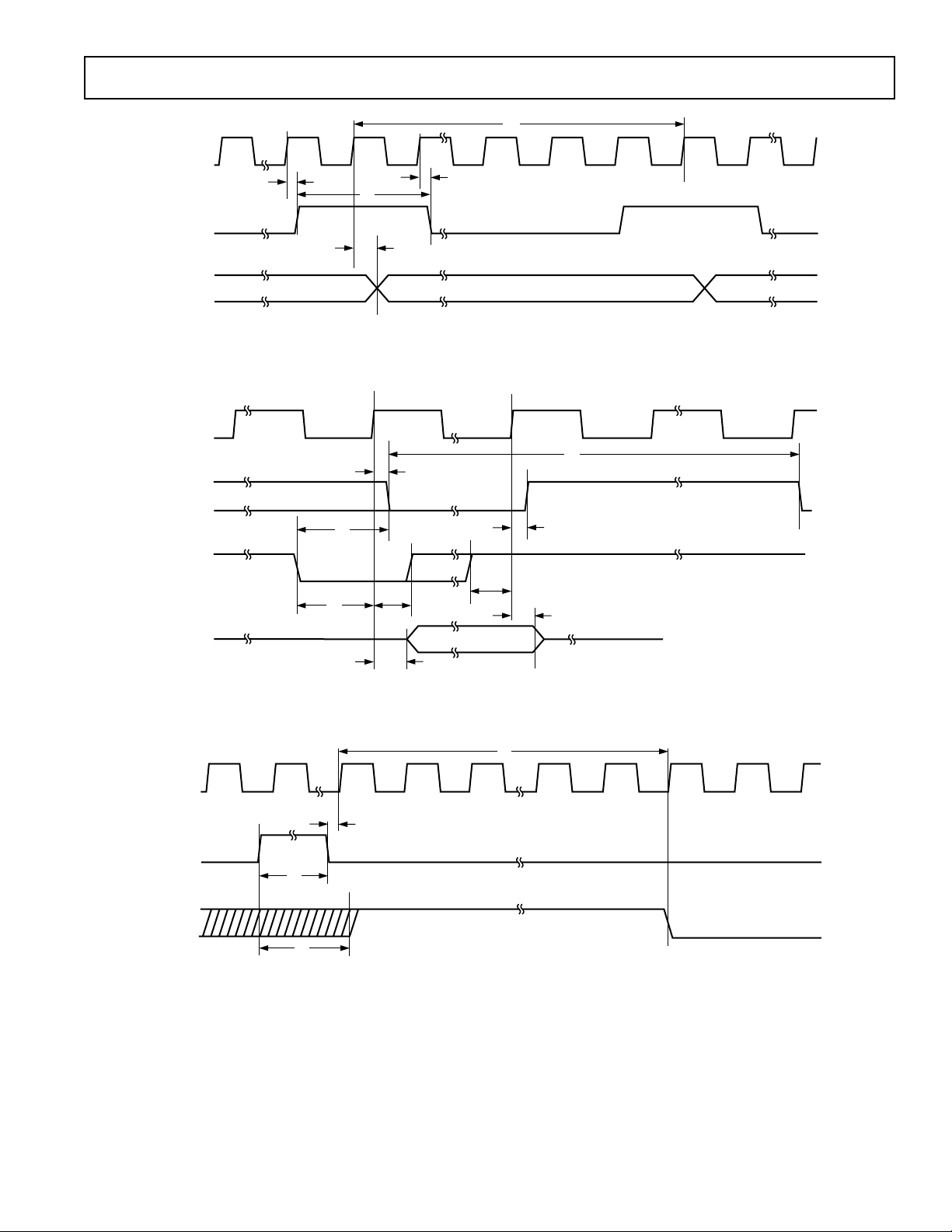
Figure 2. Serial Mode Timing for Clock Input, Frame Sync Input and Serial Clock Output
32 CLKIN CYCLES
CLKIN
t
8
FSI
t
14
SCO
t
11
FSO
(SFMT = 0)
t
11
FSO
(SFMT = 1)
SDO
t
12
t
13
D15 D14 D13 D2 D1 D0 D15 D14
Figure 3. Serial Mode 1. Timing for Frame Sync Input, Frame Sync Output, Serial Clock Output and Serial Data Output
(Refer to Table I for Control Inputs, TSI = DOE)
32 CLKIN CYCLES
CLKIN
t
8
FSI
t
SCO
(CFMT = 0)
FSO
14
t
11
t
12
t
13
SDO
D2 D1 D0 D15 D14 D13 D12 D11
D3 D2 D1 D0 D15 D14
D4
D5
Figure 4. Serial Mode 2. Timing for Frame Sync Input, Frame Sync Output, Serial Clock Output and Serial Data Output
(Refer to Table I for Control Inputs, TSI = DOE)
–5–REV. 0
AD7723
16 CLKIN CYCLES
CLKIN
t
8
FSI
t
SCO
(CFMT = 0)
FSO
SDO
Figure 5. Serial Mode 3. Timing for Frame Sync Input, Frame Sync Output, Serial Clock Output and Serial Data Output
(Refer to Table I for Control Inputs, TSI = DOE)
14
t
11
t
13
D2 D1 D0 D15 D14 D13 D12 D11 D5 D4 D3 D2 D1 D0 D15 D14
t
12
Table I. Serial Interface (Mode1 = 0, Mode2 = 0)
Decimation Digital Filter SCO Frequency Output Data Control Inputs
Serial Mode Ratio (SLDR) Mode (SLP) (SCR) Rate SLDR SLP SCR
1 32 Low Pass f
1 32 Band Pass f
2 32 Low Pass f
2 32 Band Pass f
3 16 Low Pass f
CLKIN
CLKIN
/2 f
CLKIN
/2 f
CLKIN
CLKIN
f
/32 1 1 0
CLKIN
f
/32 1 0 0
CLKIN
/32 1 1 1
CLKIN
/32 1 0 1
CLKIN
f
/16 0 1 0
CLKIN
Table II. Parallel Interface
Digital Filter Decimation Output Control Inputs
Mode Ratio Data Rate MODE1 MODE2
Band Pass 32 f
Low Pass 32 f
Low Pass 16 f
DOE
t
15
SDO
/32 0 1
CLKIN
/32 1 0
CLKIN
/16 1 1
CLKIN
t
16
Figure 6. Serial Mode Timing for Data Output Enable and Serial Data Output
–6– REV. 0
CLKIN
DRDY
AD7723
t
18
t
t
19
t
17
t
20
19
DB0–DB15
CLKIN
DRDY
RD/CS
DB0–DB15
WORD N – 1 WORD N + 1
Figure 7a. Parallel Mode Read Timing, CS and
t
19
t
22
t
t
21
22
VALID DATA
t
23
Figure 7b. Parallel Mode Read Timing, CS =
WORD N
RD
Tied Logic Low
t
18
t
19
t
21
t
24
RD
CLKIN
SYNC
DRDY
t
28
t
26
t
25
t
27
Figure 8. SYNC Timing
–7–REV. 0
 Loading...