Analog Devices AD7722 Datasheet
16-Bit, 195 kSPS
AV
DD
DV
DD
REF1
AGNDDGND
VIN(+)
VIN(–)
P/S
REF2
XTAL
CLKIN
UNI
DB15
DB14
DB12
DB11
DB10
DB9/FSO
CAL
RESET
SYNC
CS
DVAL/RD
CFMT/DRDY
DB0
DB1
DB2
DB3/
TSI
DB4/
DOE
DB5/
SFMT
DB6/
FSI
DB7/
SCO
DB8/
SDO
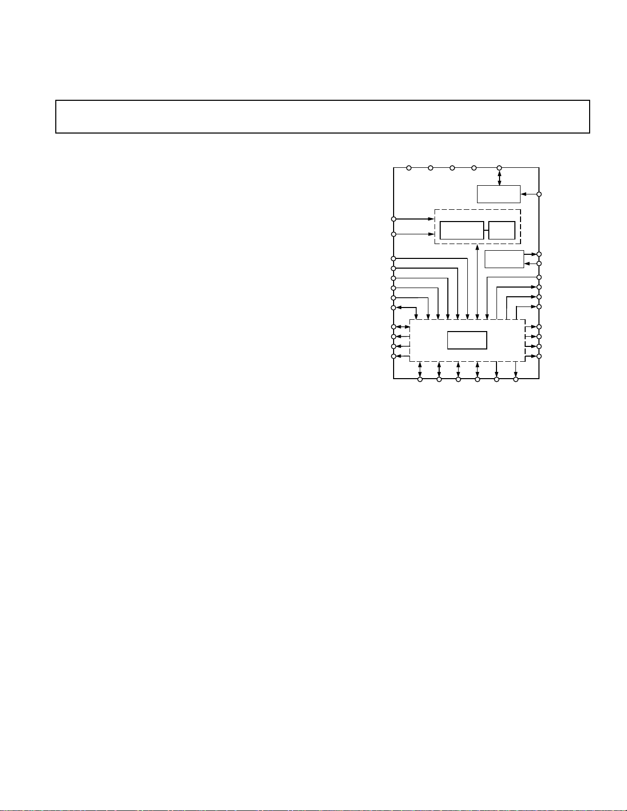
16-BIT A/D CONVERTER
Σ∆
MODULATOR
FIR
FILTER
CLOCK
CIRCUITRY
CONTROL
LOGIC
DB13
AD7722
2.5V
REFERENCE
a
FEATURES
16-Bit Sigma-Delta ADC
643 Oversampling Ratio
Up to 220 kSPS Output Word Rate
Low-Pass, Linear Phase Digital Filter
Inherently Monotonic
On-Chip 2.5 V Voltage Reference
Single Supply +5 V
High Speed Parallel or Serial Interface
GENERAL DESCRIPTION
The AD7722 is a complete low power, 16-bit, sigma-delta
ADC. The part operates from a +5 V supply and accepts a
differential input voltage range of 0 V to +2.5 V or ± 1.25 V
centered around a common-mode bias. The AD7722 provides
16-bit performance for input bandwidths up to 90.625 kHz.
The part provides data at an output word rate of 195.3 kHz.
The analog input is continuously sampled by an analog modulator eliminating the need for external sample-and-hold circuitry.
The modulator output is processed by two Finite Impulse
Response (FIR) digital filters in series. The on-chip filtering
reduces the external antialias requirements to first order, in
most cases. The group delay for the filter is 215.5 µs, while the
settling time for a step input is 431 µs. The sample rate, filter
corner frequency, and output word rate are set by an external
clock that is nominally 12.5 MHz.
Use of a single bit DAC in the modulator guarantees excellent
linearity and dc accuracy. Endpoint accuracy is ensured by onchip calibration. This calibration procedure minimizes the zeroscale and full-scale errors.
CMOS, Sigma-Delta ADC
AD7722
FUNCTIONAL BLOCK DIAGRAM
Conversion data is provided at the output register through a
flexible serial port or a parallel port. This offers 3-wire, high
speed interfacing to digital signal processors. The serial interface
operates in an internal clocking (master) mode, whereby an
internal serial data clock and framing pulse are device outputs.
Additionally, two AD7722s can be configured with the serial
data outputs connected together. Each converter alternately
transmits its conversion data on a shared serial data line.
The part provides an accurate on-chip 2.5 V reference. A
reference input/output function is provided to allow either the
internal reference or an external system reference to be used as
the reference source for the part.
The AD7722 is available in a 44-pin PQFP package and is
specified over the industrial temperature range from –40°C to
+85°C.
REV. 0
Information furnished by Analog Devices is believed to be accurate and
reliable. However, no responsibility is assumed by Analog Devices for its
use, nor for any infringements of patents or other rights of third parties
which may result from its use. No license is granted by implication or
otherwise under any patent or patent rights of Analog Devices.
One Technology Way, P.O. Box 9106, Norwood, MA 02062-9106, U.S.A.
Tel: 617/329-4700 World Wide Web Site: http://www.analog.com
Fax: 617/326-8703 © Analog Devices, Inc., 1996

1
AD7722–SPECIFICATIONS
UNI = Logic Low or High; f
= 12.5 MHz; FS = 195.3 kSPS; REF2 = +2.5 V; TA = T
CLKLIN
(AVDD = AV
Parameter Test Conditions/Comments Min Typ Max Units
INH
2
VCM = 2.5 V, VIN(+) = VIN(–) =1.25 V pk-pk
(–) =1.25 V, VIN(+) = 0 to 2.5
or, V
3
3
IN
Input Bandwidth 0 kHz–90.625 kHz 86/84.5 90 dB
Input Bandwidth 0 kHz–100 kHz, f
Input Bandwidth 0 kHz–90.625 kHz –90/–88 dB
DYNAMIC SPECIFICATIONS
Bipolar Mode, UNI = V
Signal to (Noise + Distortion)
Total Harmonic Distortion
Input Bandwidth 0 kHz–100 kHz, f
Spurious Free Dynamic Range Input Bandwidth 0 kHz–90.625 kHz –90 dB
Input Bandwidth 0 kHz–100 kHz, f
Unipolar Mode,
UNI = V
INL
Signal to (Noise + Distortion)
Total Harmonic Distortion
3
VIN(–) = 0 V, VIN(+) = 0 to 2.5
3
Input Bandwidth 0 kHz–90.625 kHz 84.5/83 88 dB
Input Bandwidth 0 kHz–97.65 kHz –89/–87 dB
Spurious Free Dynamic Range Input Bandwidth 0 kHz–97.65 kHz –90 dB
Intermodulation Distortion –93 dB
AC CMRR V
(+) = VIN(–) = 2.5 V pk-pk
IN
= 1.25 V to 3.75 V, 20 kHz 96 dB
V
CM
Digital Filter Response
Pass-Band Ripple 0 kHz–90.625 kHz ±0.005 dB
Cutoff Frequency 96.92 kHz
Stop-Band Attenuation 104.6875 kHz to 12.395 MHz 90 dB
= +5 V 6 5%; DVDD = +5 V 6 5%; AGND = AGND1 = DGND = 0 V;
DD1
to T
MIN
; unless otherwise noted)
MAX
A Version
= 14 MHz 84.5/83 dB
CLKIN
= 14 MHz –88/–86 dB
CLKIN
= 14 MHz –88 dB
CLKIN
ANALOG INPUTS
Full-Scale Input Span V
Bipolar Mode
Unipolar Mode
Absolute Input Voltage V
(+)–VIN(–)
IN
UNI = V
UNI = V
INH
INL
(+) and VIN(–) 0 AV
IN
–V
/2 +V
REF2
0V
REF2
REF2
DD
/2 V
V
V
Input Sampling Capacitance 2pF
Input Sampling Rate Guaranteed by Design 2 × f
CLKIN
Differential Input Impedance 1/8E-09 × f
CLKIN
Hz
kΩ
CLOCK
CLKIN Mark Space Ratio 45 55 %
REFERENCE
REF1 Output Voltage 2.32 2.47 2.62 V
REF1 Output Voltage Drift 60 ppm/°C
REF1 Output Impedance 3kΩ
Reference Buffer
Offset Voltage Offset Between REF1 and REF2 ±12 mV
Using Internal Reference
REF2 Output Voltage 2.32 2.47 2.62 V
REF2 Output Voltage Drift 60 ppm/°C
Using External Reference
REF2 Input Impedance REF1 = AGND 1/16E-09 ×f
CLKIN
kΩ
External Reference Voltage Range Applied to REF1 or REF2 2.32 2.5 2.62 V
STATIC PERFORMANCE
Resolution 16 Bits
Differential Nonlinearity Guaranteed Monotonic ± 0.5 ± 1 LSB
Integral Nonlinearity ±2 LSB
After Calibration
Offset Error
Gain Error
4, 5
4
±3mV
±0.6 % FSR
Without Calibration
Offset Error ±6mV
Gain Error
5
±0.6 % FSR
Offset Error Drift ±1 LSB/°C
Gain Error Drift REF2 Is an Ideal Reference, REF1 = AGND
Unipolar Mode ±1 LSB/°C
Bipolar Mode ±0.5 LSB/°C
–2–
REV. 0
AD7722
WARNING!
ESD SENSITIVE DEVICE
I
OL
1.6mA
I
OH
200µA
+1.6V
C
L
50pF
TO
OUTPUT
PIN
Parameter Test Conditions/Comments Min Typ Max Units
A Version
LOGIC INPUTS (Excluding CLKIN)
, Input High Voltage 2.0 V
V
INH
V
, Input Low Voltage 0.8 V
INL
CLOCK INPUT (CLKIN)
, Input High Voltage 4.0 V
V
INH
V
, Input Low Voltage 0.4 V
INL
ALL LOGIC INPUTS
, Input Current VIN = 0 V to DV
I
IN
DD
±10 µA
CIN, Input Capacitance 10 pF
LOGIC OUTPUTS
, Output High Voltage |I
V
OH
VOL, Output Low Voltage |I
| = 200 µA 4.0 V
OUT
| = 1.6 mA 0.4 V
OUT
POWER SUPPLIES
AV
DV
I
DD
DD
DD
, AV
DD1
Total from AVDD and DV
DD
4.75 5.25 V
4.75 5.25 V
75 mA
Power Consumption 375 mW
NOTES
1
Operating temperature range is as follows : A Version ; –40°C to +85°C.
2
Measurement Bandwidth = 0.5 × FS; Input Level = –0.05 dB.
3
TA = +25°C to +85°C/TA = T
4
Applies after calibration at temperature of interest.
5
Gain Error excludes reference error. The ADC gain is calibrated w.r.t. the voltage on the REF2 pin.
Specifications subject to change without notice.
MIN
to T
MAX
.
ABSOLUTE MAXIMUM RATINGS*
(TA = +25°C unless otherwise noted)
DVDD to DGND . . . . . . . . . . . . . . . . . . . . . . . . –0.3 V to 7 V
AV
AV
DD
DD
, AV
, AV
to AGND . . . . . . . . . . . . . . . . . . –0.3 V to 7 V
DD1
to DVDD . . . . . . . . . . . . . . . . . . . –1 V to +1 V
DD1
Model Temperature Package Package
AD7722AS –40°C to +85°C 44-Pin PQFP S-44
ORDERING GUIDE
AGND, AGND1 to DGND . . . . . . . . . . . . . –0.3 V to +0.3 V
Digital Inputs to DGND . . . . . . . . . . –0.3 V to DV
Digital Outputs to DGND . . . . . . . . . –0.3 V to DV
V
(+), VIN(–) to AGND . . . . . . . . . . –0.3 V to AVDD + 0.3 V
IN
REF1 to AGND . . . . . . . . . . . . . . . . –0.3 V to AV
REF2 to AGND . . . . . . . . . . . . . . . . –0.3 V to AV
+ 0.3 V
DD
+ 0.3 V
DD
+ 0.3 V
DD
+ 0.3 V
DD
DGND, AGND1, AGND2 . . . . . . . . . . . . . . . . . . . . . ±0.3 V
Operating Temperature Range . . . . . . . . . . . –40°C to +85°C
Storage Temperature Range . . . . . . . . . . . . –65°C to +150°C
Junction Temperature . . . . . . . . . . . . . . . . . . . . . . . . .+150°C
θ
Thermal Impedance . . . . . . . . . . . . . . . . . . . . . . . 95°C/W
JA
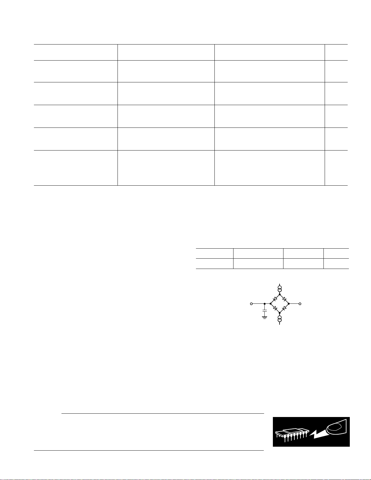
Figure 1. Load Circuit for Timing Specifications
Lead Temperature, Soldering
Vapor Phase (60 sec) . . . . . . . . . . . . . . . . . . . . . . . .+215°C
Infrared (15 sec) . . . . . . . . . . . . . . . . . . . . . . . . . . . .+220°C
*Stresses above those listed under “Absolute Maximum Ratings” may cause
permanent damage to the device. This is a stress rating only and functional
operation of the device at these or any other conditions above those indicated in the
operational section of this specification is not implied. Exposure to absolute
maximum rating conditions for extended periods may affect device reliability.
CAUTION
ESD (electrostatic discharge) sensitive device. Electrostatic charges as high as 4000 V readily
accumulate on the human body and test equipment and can discharge without detection.
Although the AD7722 features proprietary ESD protection circuitry, permanent damage may
occur on devices subjected to high energy electrostatic discharges. Therefore, proper ESD
precautions are recommended to avoid performance degradation or loss of functionality.
REV. 0
–3–
AD7722
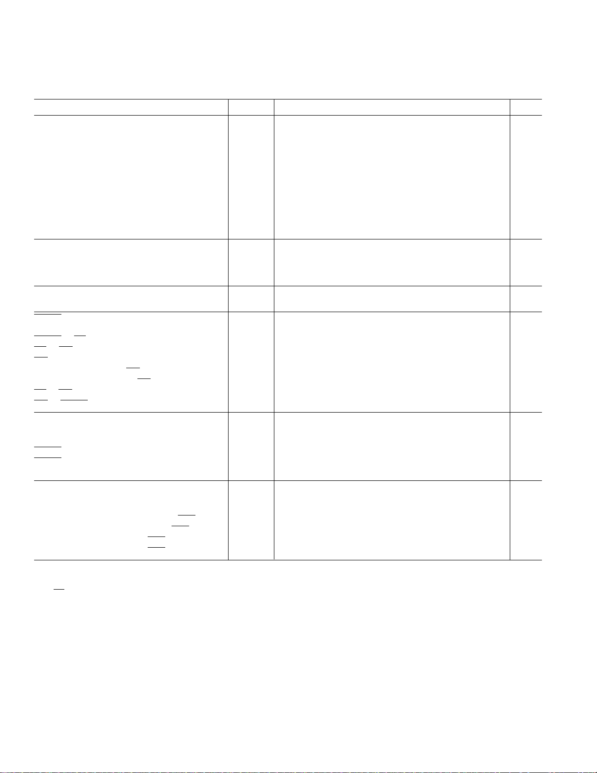
(AVDD= +5 V 6 5%, DVDD = +5 V 6 5%, AGND = DGND = 0 V, CL = 50 pF, TA = T
f
TIMING SPECIFICATIONS
= 12.5 MHz, SFMT = Logic Low or High, CFMT = Logic Low or High)
CLKIN
CLKIN Frequency f
CLKIN Period (t
CLK
= 1/f
)t
CLK
CLKIN Low Pulse Width t
CLKIN High Pulse Width t
CLKIN Rise Time t
CLKIN Fall Time t
FSI Low Time t
FSI Setup Time t
FSI Hold Time t
CLKIN to SCO Delay t
SCO Period
1
SCO Transition to FSO High Delay t
SCO Transition to FSO Low Delay t
SCO Transition to SDO Valid Delay t
SCO Transition from FSI
2
SDO Enable Delay Time t
SDO Disable Delay Time t
DRDY High Time t
Conversion Time
1
DRDY to CS Setup Time t
CS to RD Setup Time t
RD Pulse Width t
Data Access Time after
Bus Relinquish Time after
RD Falling Edge
RD Rising Edge t
3
CS to RD Hold Time t
RD to DRDY High Time t
SYNC/RESET Input Pulse Width t
DVAL Low Delay from SYNC/RESET t
SYNC/RESET Low Time Before CLKIN Rising t
DRDY High Delay after SYNC/RESET Low t
DRDY Low Delay after SYNC/RESET Low1t
DVAL High Delay after SYNC/RESET Low1t
CAL Setup Time t
CAL Pulse Width t
Calibration Delay from CAL High t
Unipolar Input Calibration Time, (UNI = “0”)1t
Bipolar Input Calibration Time, (UNI = “1”)1t
Conversion Results Valid, (UNI = “0”)
Conversion Results Valid, (UNI = “1”)
NOTES
1
Guaranteed by design.
2
Frame Sync is initiated on falling edge of CLKIN.
3
With RD synchronous to CLKIN t22, can be reduced up to 1 t
1
1
CLK
to T
MAX
,
MIN
Symbol Min Typ Max Units
CLK
1
2
3
4
5
6
7
8
9
t
10
11
12
13
t
14
15
16
17
t
18
19
20
21
t
22
23
24
25
26
27
28
29
30
31
34
35
36
37
37
t
38
t
38
.
0.3 12.5 15 MHz
0.067 0.08 3.33 µs
0.45 × t
0.45 × t
1
1
0.55 × t
0.55 × t
1
1
5ns
5ns
2t
CLK
20 ns
20 ns
40 ns
2t
CLK
410 ns
410 ns
38 ns
2.5 t
CLK
30 45 ns
10 30 ns
2t
64 t
CLK
CLK
0ns
0ns
t
+ 20 ns
CLK
t
+ 40 ns
CLK
t
+ 40 ns
CLK
0ns
1t
CLK
10 ns
40 ns
10 ns
50 ns
(8192 + 64) t
8192 t
CLK
CLK
10 ns
12 t
64 t
(3 × 8192 + 2 × 512) t
(4 × 8192 + 3 × 512) t
(3 × 8192 + 2 × 512 + 64) t
(4 × 8192 + 3 × 512 + 64) t
CLK
CLK
CLK
CLK
CLK
CLK
–4–
REV. 0
CLKIN
SCO
(CFMT = 0)
FSO
(SFMT = 0)
AD7722
64 CKLIN CYCLES
32 SCO CYCLES
SCO
ZERO FOR LAST 16 SCO CYCLESVALID DATA FOR 16 SCO CYCLES VALID
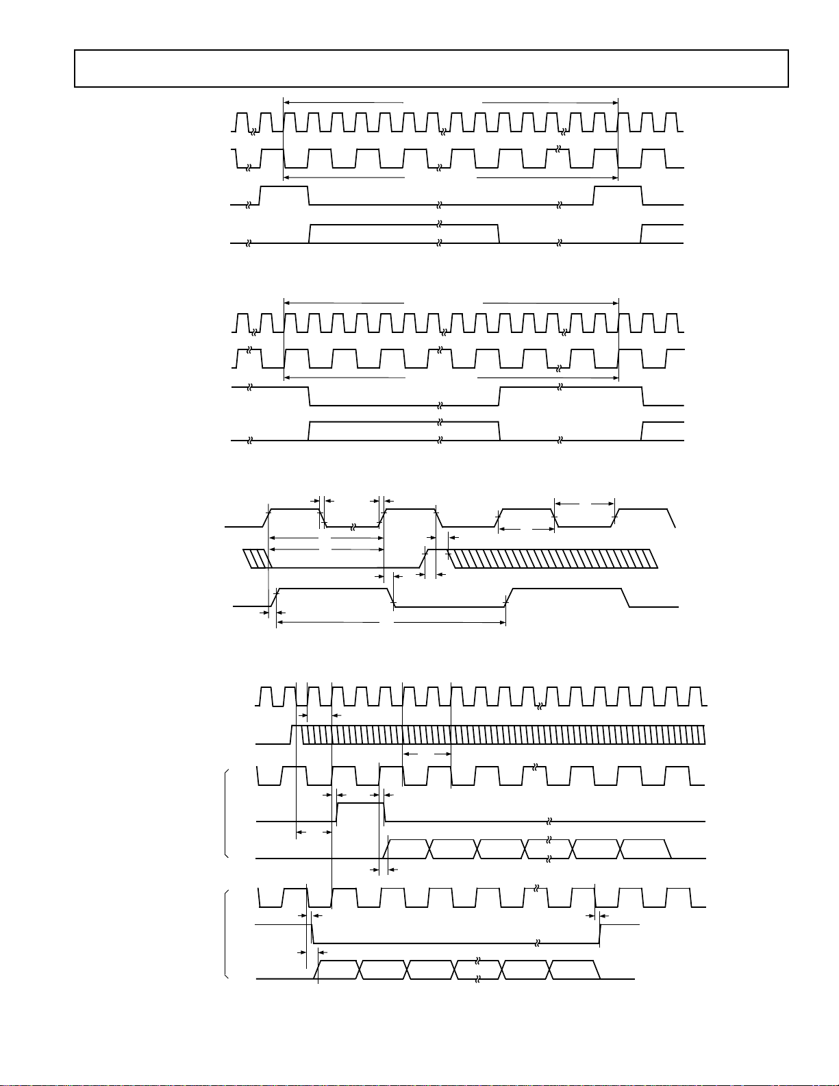
Figure 2a. Generalized Serial Mode Timing (FSI = Logic Low or High, TSI = DOE)
64 CKLIN CYCLES
CLKIN
SCO
(CFMT = 0)
FSO
(SFMT = 1)
SCO
LOW FOR 16 SCO CYCLES
VALID DATA FOR 16 SCO CYCLES
32 SCO CYCLES
HIGH FOR LAST 16 SCO CYCLES
ZERO FOR LAST 16 SCO CYCLES
Figure 2b. Generalized Serial Mode Timing (FSI = Logic Low or High, TSI = DOE)
t
4
t
t
8
t
9
t
10
t
7
3
t
2
CLKIN
FSI
SCO
2.3V
t
5
0.8V
t
1
t
6
t
9
VALID
Figure 3. Serial Mode Timing for Clock Input, Frame Sync Input and Serial Clock Output
CLKIN
t
1
FSI
t
10
SCO
SFMT = LOGIC
LOW(0)
SFMT = LOGIC
HIGH(1)
FSO
SDO
SCO
FSO
SDO
LOW FOR
D15–D0
t
11
t
14
t
12
t
13
D15 D14 D13 D1 D0
t
12
D15 D14 D13 D1 D0
t
13
t
11
Figure 4. Serial Mode Timing for Frame Sync Input, Frame Sync Output, Serial Clock Output
and Serial Data Output (CFMT = Logic Low, TSI = DOE)
REV. 0
–5–
AD7722
DOE
t
16
SDO
t
15
Figure 5. Serial Mode Timing for Data Output Enable and Serial Data Output (TSI = Logic Low)
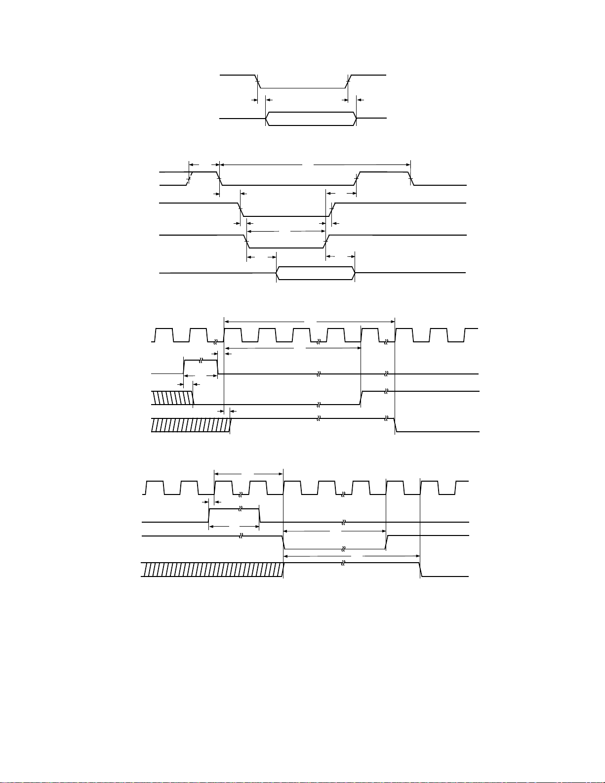
DRDY
t
17
t
19
t
18
t
25
DB0 – DB15
CLKIN
SYNC, RESET
DVAL
DRDY
CLKIN
CAL
DVAL
DRDY
CS
RD
t
20
t
21
t
22
VALID DATA
t
24
t
23
Figure 6. Parallel Mode Read Timing
t
30
t
t
28
t
t
27
26
t
29
31
Figure 7. SYNC and RESET Timing, Serial and Parallel Mode
t
36
t
34
t
35
t
37
t
38
Figure 8. Calibration Timing, Serial and Parallel Mode
–6–
REV. 0

PIN FUNCTION DESCRIPTION
Mnemonic Pin No. Description
AD7722
AV
DD1
14 Clock logic power supply voltage for the analog modulator, +5 V ± 5%.
AGND1 10 Clock logic ground reference for the analog modulator.
AV
DD
20, 23 Analog Power Supply Voltage, +5 V ± 5%.
AGND 9, 13, 15, Ground reference for analog circuitry.
19, 21, 25, 26
DV
DD
39 Digital Power Supply Voltage, +5 V ± 5%.
DGND 6, 28 Ground reference for digital circuitry.
REF1 22 Reference Input/Output. REF1 connects through 3 kΩ to the output of the internal 2.5 V
reference and to the input of a buffer amplifier that drives the Σ−∆ modulator. This pin can
also be overdriven with an external reference 2.5 V.
REF2 24 Reference Input/Output. REF2 connects to the output of an internal buffer amplifier used to
to drive the Σ−∆ modulator. When REF2 is used as an input, REF1 must be connected
to AGND.
V
(+) 18 Positive terminal of the differential analog input.
IN
V
(–) 16 Negative terminal of the differential analog input.
IN
UNI 7 Analog input range select input. UNI selects the analog input range for either bipolar
or unipolar operation. A logic low input selects unipolar operation. A logic high input
selects bipolar operation.
CLKIN 11 Clock Input. Master clock signal for the device. The CLKIN pin interfaces the AD7722
internal oscillator circuit to an external crystal or to an external clock. A parallel resonant,
fundamental-frequency, microprocessor-grade crystal and a 1 MΩ resistor should be
connected between the CLKIN and XTAL pin with two capacitors connected from each
pin to ground. Alternatively, the CLKIN pin can be driven with an external CMOScompatible clock. The AD7722 is specified with a clock input frequency of 12.5 MHz.
XTAL 12 Oscillator Output. The XTAL pin connects the internal oscillator output to an external
crystal. If an external clock is used, XTAL should be left unconnected.
P/
S 8 Parallel/Serial interface select input. A logic high configures output data interface for parallel
mode operation. Serial mode operation is selected with the P/S set to a logic low.
CAL 27 Calibration Logic Input. A logic high input for a duration of one CLKIN cycle initiates a
calibration sequence for the device Gain and Offset Error.
RESET 17 Reset Logic Input. RESET is used to clear the offset and gain calibration registers. RESET is an
asynchronous input. RESET allows the user to set AD7722 to an uncalibrated state if the device
had been previously calibrated. A rising edge also resets the AD7722 Σ−∆ modulator by shorting
the integrator capacitors in the modulator. In addition RESET functions identically to the
SYNC pin described below.
CS 29 Chip select is a level sensitive logic input. CS enables the output data register for parallel mode
read operation. The CS logic level is sensed on the rising edge of CLKIN. The output data bus
is enabled when the rising edge of CLKIN senses a logic low level on CS if RD is also low. When
CS is sensed high, the output data bits DB15–DB0 will be high impedance. In serial mode tie
CS to a logic low.
SYNC 30 Synchronization Logic Input. SYNC is an asynchronous input. When using more than one
AD7722 operated from a common master clock, SYNC allows each ADC’s Σ−∆ modulator
to simultaneously sample its analog input and update its output data register. A rising edge resets
the AD7722 digital filter sequencer counter to zero. After a SYNC, conversion data is not valid
until after the digital filter settles (reference Figure 7). DVAL goes low in the serial mode. When
the rising edge of CLKIN senses a logic low on SYNC (or RESET) the reset state is released; in
parallel mode,
8192 CLKIN cycles (128 × 64/f
convolution cycle of the digital filter (64 CLKIN periods), when valid data is ready to be read
from the output data register.
DRDY goes high. After the reset state is released, DVAL returns high after
); in parallel mode, DRDY returns low after one additional
CLKIN
REV. 0
–7–

AD7722
PIN CONFIGURATION
44-Pin PQFP (S-44)
DD
DV
SCO/DB7
FSI/DB6
40 39 3841424344 36 35 3437
AD7722
TOP VIEW
(Not to Scale)
VIN(–)
AGND
RESET
FSO/DB9
SDO/DB8
VIN(+)
AGND
DGND/DB10
DGND/DB11
DGND/DB12
DD
REF1
AV
AGND
33
DGND/DB13
32
DGND/DB14
31
DGND/DB15
30
SYNC
CS
29
28
DGND
27
CAL
26
AGND
25
AGND
24
REF2
23
AV
DD
DGND/DB2
DGND/DB1
DGND/DB0
CFMT/DRDY
DVAL/RD
DGND
UNI
P/S
AGND
AGND1
CLKIN
TSI/DB3
SFMT/DB5
DOE/DB4
1
PIN 1
IDENTIFIER
2
3
4
5
6
7
8
9
10
11
121314 15 16 17 18 192021 22
DD1
XTAL
AGND
AV
PARALLEL MODE PIN FUNCTION DESCRIPTION
Mnemonic Pin No. Description
DVAL/
RD 5 Read Input is a level sensitive logic input. The RD logic level is sensed on the rising edge of CLKIN.
This digital input can be used in conjunction with
bus is enabled when the rising edge of CLKIN senses a logic low level on
CS to read data from the device. The output data
RD if CS is also low. When
RD is sensed high, the output data bits DB15–DB0 will be high impedance.
CFMT/
DRDY 2 Data Ready Logic Output. A falling edge indicates a new output word is available to be read from out-
put data register. DRDY will return high upon completion of a read operation. If a read operation
does not occur between output updates, DRDY will pulse high for two CLKIN cycles before the next
output update. DRDY also indicates when conversion results are available after a SYNC or RESET
sequence and when completing a self-calibration.
DGND/DB15 31 Data Output Bit (MSB)
DGND/DB14 32 Data Output Bit
DGND/DB13 33 Data Output Bit
DGND/DB12 34 Data Output Bit
DGND/DB11 35 Data Output Bit
DGND/DB10 36 Data Output Bit
FSO/DB9 37 Data Output Bit
SDO/DB8 38 Data Output Bit
SCO/DB7 40 Data Output Bit
FSI/DB6 41 Data Output Bit
SFMT/DB5 42 Data Output Bit
DOE/DB4 43 Data Output Bit
TSI/DB3 44 Data Output Bit
DGND/DB2 1 Data Output Bit
DGND/DB1 2 Data Output Bit
DGND/DB0 3 Data Output Bit (LSB)
–8–
REV. 0
 Loading...