Analog Devices AD7721 Datasheet

CMOS 16-Bit,
a
FEATURES
16-Bit Sigma-Delta ADC
468.75 kHz Output Word Rate (OWR)
No Missing Codes
Low-Pass Digital Filter
High Speed Serial Interface
Linear Phase
229.2 kHz Input Bandwidth
Power Supplies: AV
Standby Mode (70 mW)
Parallel Mode (12-Bit/312.5 kHz OWR)
GENERAL DESCRIPTION
The AD7721 is a complete low power, 12-/16-bit, sigma-delta
ADC. The part operates from a +5 V supply and accepts a
differential input of 0 V to 2.5 V or ± 1.25 V. The analog input
is continuously sampled by an analog modulator at twice the
clock frequency eliminating the need for external sample-andhold circuitry. The modulator output is processed by two finite
impulse response (FIR) digital filters in series. The on-chip
filtering reduces the external antialias requirements to first order
in most cases. Settling time for a step input is 97.07 µs while
the group delay for the filter is 48.53 µs when the master clock
equals 15 MHz.
The AD7721 can be operated with input bandwidths up to
229.2 kHz. The corresponding output word rate is 468.75 kHz.
The part can be operated with lower clock frequencies also.
The sample rate, filter corner frequency and output word rate
will be reduced also, as these are proportional to the external
clock frequency. The maximum clock frequencies in parallel
mode and serial mode are 10 MHz and 15 MHz respectively.
, DVDD: +5 V 6 5%
DD
468.75 kHz, Sigma-Delta ADC
AD7721
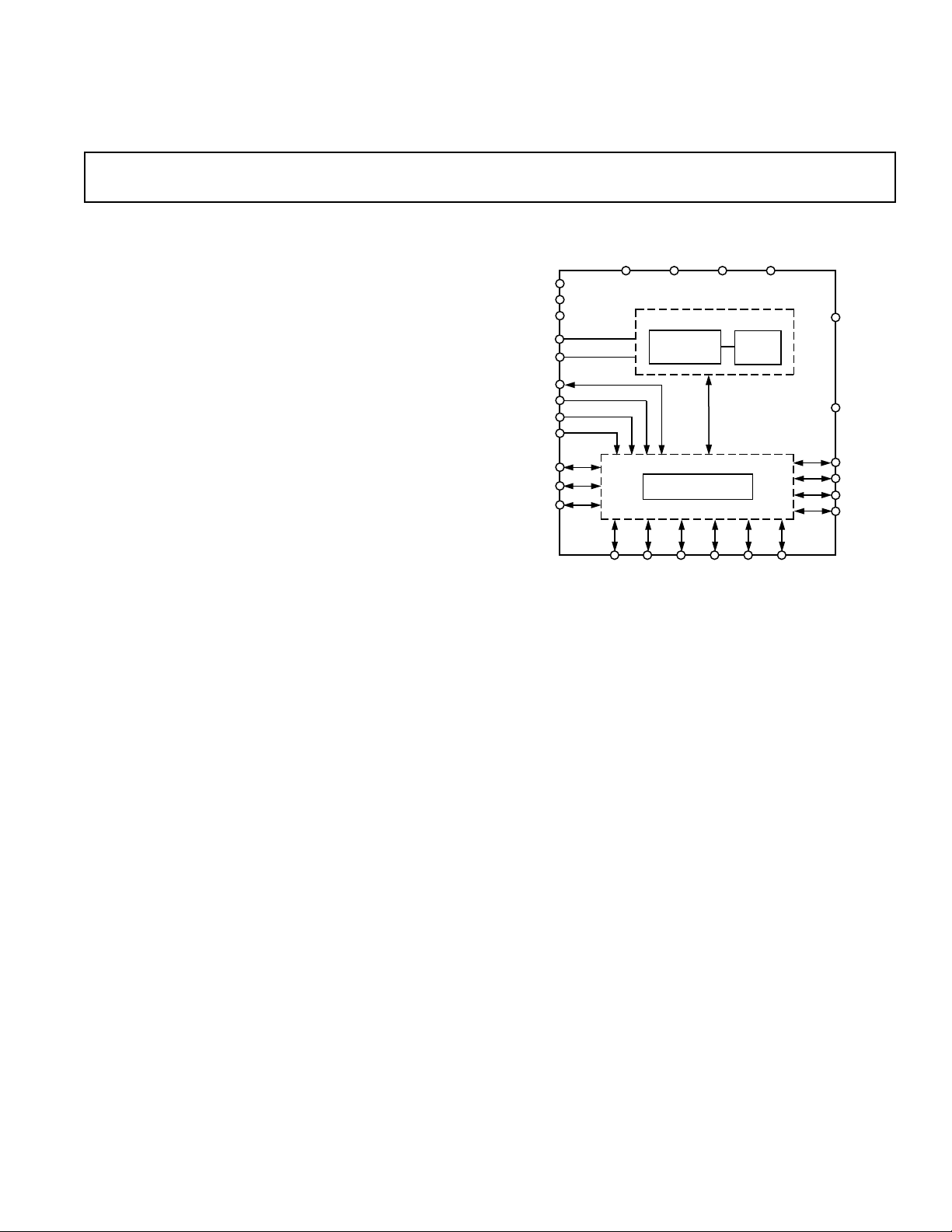
FUNCTIONAL BLOCK DIAGRAM
DD
FIR
FILTER
DB7
DV
DD
REFIN
CLK
DRDY
SDATA/DB11
RFS/DB10
DB9
DB8
S-D
SYNC/
DB5
AV
DB6 SCLK/
DGND
DGND
DSUBST
VIN1
VIN2
DVAL/SYNC
CS
RD
WR
STBY/DB0
CAL/DB1
UNI/DB2
AGND
AD7721
DB3
AGND
12-BIT A/D CONVERTER
MODULATOR
CONTROL LOGIC
DB4
Use of a single bit DAC in the modulator guarantees excellent
linearity and dc accuracy. Endpoint accuracy is ensured by onchip calibration of offset and gain. This calibration procedure
minimizes the part’s zero-scale and full-scale errors.
The output data is accessed from the output register through a
serial or parallel port. This offers easy, high speed interfacing to
modern microcontrollers and digital signal processors. The
serial interface operates in internal clocking (master) mode, the
AD7721 providing the serial clock.
CMOS construction ensures low power dissipation while a
power-down mode reduces the power consumption to only
100 µW.
REV. A
Information furnished by Analog Devices is believed to be accurate and
reliable. However, no responsibility is assumed by Analog Devices for its
use, nor for any infringements of patents or other rights of third parties
which may result from its use. No license is granted by implication or
otherwise under any patent or patent rights of Analog Devices.
One Technology Way, P.O. Box 9106, Norwood, MA 02062-9106, U.S.A.
Tel: 781/329-4700 World Wide Web Site: http://www.analog.com
Fax: 781/326-8703 © Analog Devices, Inc., 1997

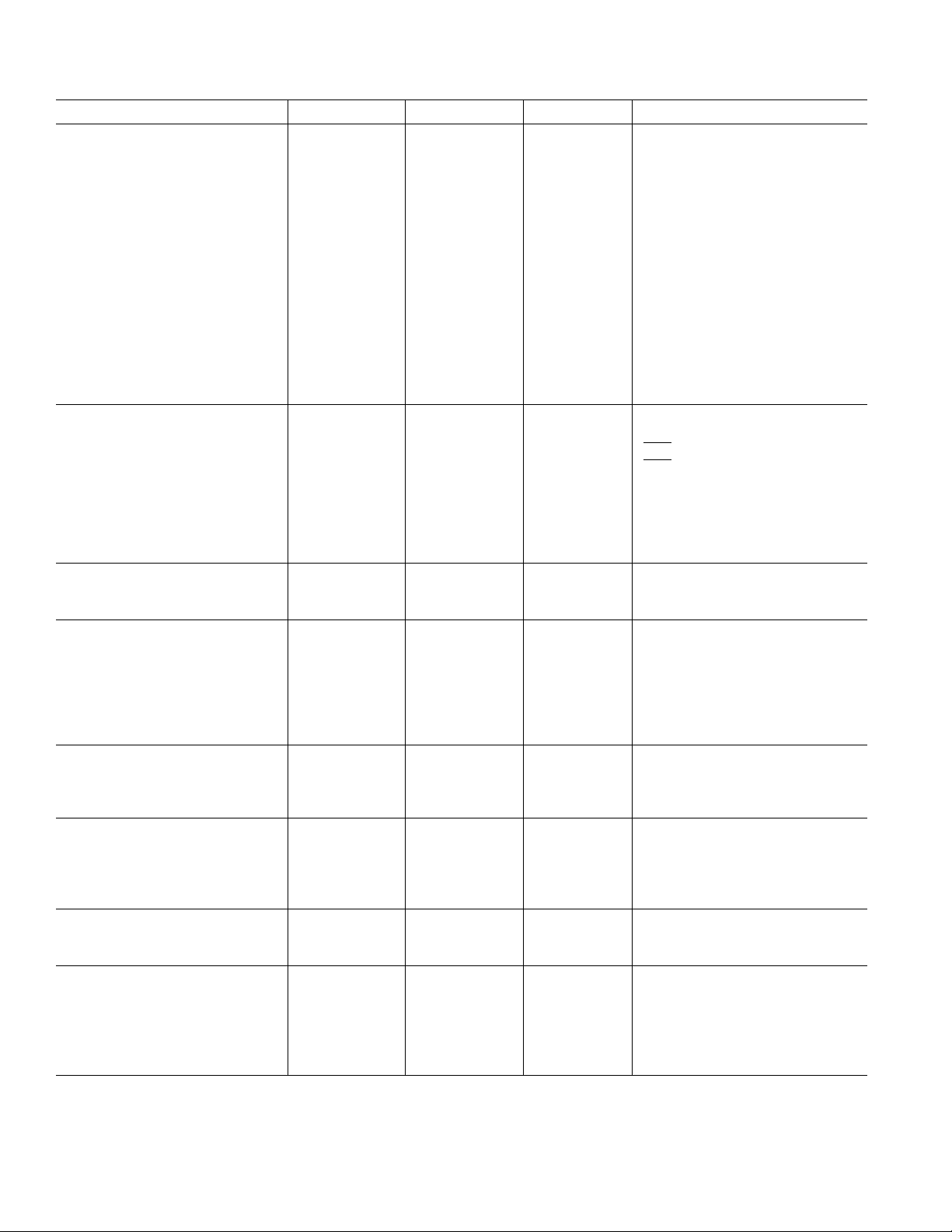
(AVDD = +5 V 6 5%; DVDD = +5 V 6 5%; AGND = DGND = 0 V,
AD7721–SPECIFICA TIONS
1
f
= 15 MHz, REFIN = +2.5 V; TA = T
CLK
MIN
to T
, unless otherwise noted)
MAX
Parameter A Version S Version Units Test Conditions/Comments
SERIAL MODE ONLY
STATIC PERFORMANCE
Resolution 16 16 Bits
Minimum Resolution for Which 12 12 Bits min Guaranteed 12 Bits Monotonic
No Missing Codes Is Guaranteed
Differential Nonlinearity ±8 ±8 LSB typ
Integral Nonlinearity ±16 ± 16 LSB max 16-Bit Operation
DC CMRR 70 70 dB min Bipolar Mode
Offset Error
2
Unipolar Mode ±3.66 ±3.66 mV max Typically 0.61 mV
Bipolar Mode ±3.66 ±3.66 mV max Typically 0.61 mV
Full-Scale Error
2, 3
Unipolar Mode ±4.88 ±4.88 mV max Typically 0.61 mV
Bipolar Mode ±4.88 ±4.88 mV max Typically 1.22 mV
Unipolar Offset Drift 0.05 0.05 mV/°C typ
Bipolar Offset Drift 0.04 0.04 mV/°C typ
ANALOG INPUTS
Signal Input Span (VIN1–VIN2)
Bipolar Mode ±V
Unipolar Mode 0 to V
Maximum Input Voltage AV
/2 ±V
REFIN
REFIN
DD
REFIN
0 to V
AV
DD
/2 Volts max UNI = V
REFIN
Volts max UNI = V
Volts
IH
IL
Minimum Input Voltage 0 0 Volts
Input Sampling Capacitance 1.6 1.6 pF typ
Input Sampling Rate 2 f
CLK
2 f
CLK
MHz Guaranteed by Design
Differential Input Impedance 20.8 20.8 kΩ typ With 15 MHz on CLK Pin
REFERENCE INPUTS
V
REFIN
2.4 to 2.6 2.4 to 2.6 V min/V max
REFIN Input Current 200 200 µA typ
DYNAMIC SPECIFICATIONS
Signal to (Noise + Distortion) 74 74 dB min Input Bandwidth 0 kHz to 210 kHz
Total Harmonic Distortion –78 –78 dB max Input Bandwidth 0 kHz to 229.2 kHz
Frequency Response
0 kHz–210 kHz ±0.05 ±0.05 dB max
229.2 kHz –3 –3 dB min
259.01 kHz to 14.74 MHz –72 –72 dB min
CLOCK
CLK Duty Ratio 45 to 55 45 to 55 % max For Specified Operation
V
, CLK High Voltage 0.7 × DV
CLKH
V
, CLK Low Voltage 0.3 × DV
CLKL
DD
DD
0.7 × DV
0.3 × DV
DD
DD
V min CLK Uses CMOS Logic
V max
LOGIC INPUTS
V
, Input High Voltage 2.0 2.0 V min
INH
V
, Input Low Voltage 0.8 0.8 V max
INL
I
, Input Current 10 10 µA max
INH
CIN, Input Capacitance 10 10 pF max
LOGIC OUTPUTS
, Output High Voltage 4.0 4.0 V min |I
V
OH
VOL, Output Low Voltage 0.4 0.4 V max |I
| ≤ 200 µA
OUT
| ≤ 1.6 mA
OUT
POWER SUPPLIES
AV
DD
DV
DD
I
(Total from AVDD, DVDD) 28.5 28.5 mA max Digital Inputs Equal to 0 V or DV
DD
4.75/5.25 4.75/5.25 V min/V max
4.75/5.25 4.75/5.25 V min/V max
Power Consumption 150 150 mW max Active Mode
Power Consumption 100 100 µW max Standby Mode
NOTES
1
Operating temperature range is as follows: A Version: –40°C to +85°C; S Version: –55°C to +125°C.
2
Applies after calibration at temperature of interest.
3
Full-scale error applies to both positive and negative full-scale error. The ADC gain is calibrated w.r.t. the voltage on the REFIN pin.
Specifications subject to change without notice.
DD
–2–
REV. A

SPECIFICA TIONS
(AVDD = +5 V 6 5%; DVDD = +5 V 6 5%; AGND = DGND = 0 V, f
1
REFIN = +2.5 V; TA = T
MIN
to T
, unless otherwise noted)
MAX
= 10 MHz,
CLK
AD7721
Parameter A Version S Version Units Test Conditions/Comments
PARALLEL MODE ONLY
STATIC PERFORMANCE
Resolution 12 12 Bits
Minimum Resolution for Which 12 12 Bits min Guaranteed 12 Bits Monotonic
No Missing Codes Is Guaranteed
Differential Nonlinearity ±1/2 ±1/2 LSB typ
Integral Nonlinearity ± 1/2 ±1/2 LSB typ 12-Bit Operation
DC CMRR 70 70 dB min Bipolar Mode
Offset Error
2
Unipolar Mode ±3.66 ±3.66 mV max Typically 0.61 mV
Bipolar Mode ±3.66 ±3.66 mV max Typically 0.61 mV
Full-Scale Error
2, 3
Unipolar Mode ±4.88 ±4.88 mV max Typically 0.61 mV
Bipolar Mode ±4.88 ±4.88 mV max Typically 1.22 mV
Unipolar Offset Drift 0.04 0.04 mV/°C typ
Bipolar Offset Drift 0.035 0.035 mV/°C typ
ANALOG INPUTS
Signal Input Span (VIN1–VIN2):
Bipolar Mode ±V
Unipolar Mode 0 to V
Maximum Input Voltage AV
/2 ±V
REFIN
REFIN
DD
0 to V
AV
/2 Volts max UNI = V
REFIN
REFIN
DD
Volts max UNI = V
Volts
IH
IL
Minimum Input Voltage 0 0 Volts
Input Sampling Capacitance 1.6 1.6 pF typ
Input Sampling Rate 2 f
CLK
2 f
CLK
MHz Guaranteed by Design
Differential Input Impedance 31.25 31.25 kΩ typ With 10 MHz on CLK Pin
REFERENCE INPUTS
V
REFIN
2.4 to 2.6 2.4 to 2.6 V min/V max
REFIN Input Current 200 200 µA typ
DYNAMIC SPECIFICATIONS
Signal to (Noise + Distortion) 70 70 dB min Input Bandwidth 0 kHz to 140 kHz
Total Harmonic Distortion –78 –78 dB max Input Bandwidth 0 kHz to 152.8 kHz
Frequency Response
0 kHz–140 kHz ±0.05 ±0.05 dB max
152.8 kHz –3 –3 dB min
172.67 kHz to 9.827 MHz –72 –72 dB min
CLOCK
CLK Duty Ratio 45 to 55 45 to 55 % max For Specified Operation
, CLK High Voltage 0.7 × DV
V
CLKH
V
, CLK Low Voltage 0.3 × DV
CLKL
DD
DD
0.7 × DV
0.3 × DV
DD
DD
V min CLK Uses CMOS Logic
V max
LOGIC INPUTS
, Input High Voltage 2.0 2.0 V min
V
INH
V
, Input Low Voltage 0.8 0.8 V max
INL
, Input Current 10 10 µA max
I
INH
CIN, Input Capacitance 10 10 pF max
LOGIC OUTPUTS
, Output High Voltage 4.0 4.0 V min |I
V
OH
V
, Output Low Voltage 0.4 0.4 V max |I
OL
| ≤ 200 µA
OUT
| ≤ 1.6 mA
OUT
POWER SUPPLIES
AV
DD
DV
DD
(Total from AVDD, DVDD) 28.5 28.5 mA max
I
DD
4.75/5.25 4.75/5.25 V min/V max
4.75/5.25 4.75/5.25 V min/V max
Digital Inputs Equal to 0 V or DV
Power Consumption 150 150 mW max Active Mode
Power Consumption 100 100 µW max Standby Mode
NOTES
1
Operating temperature range is as follows: A Version: –40° C to +85°C; S Version: –55 °C to +125 °C.
2
Applies after calibration at temperature of interest.
3
Full-scale error applies to both positive and negative full-scale error. The ADC gain is calibrated w.r.t. the voltage on the REFIN pin.
Specifications subject to change without notice.
DD
REV. A
–3–

AD7721
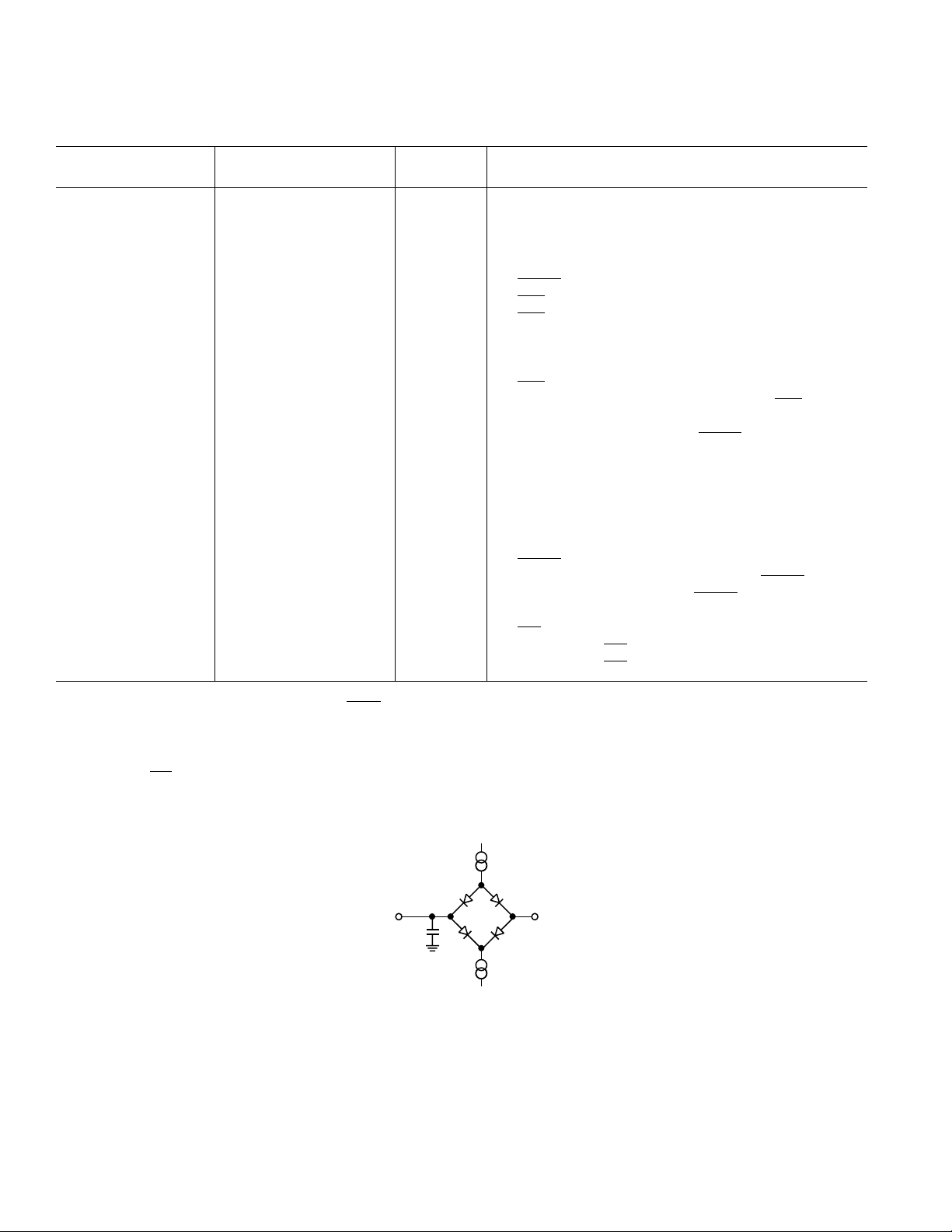
TIMING CHARACTERISTICS
(AVDD= +5 V 6 5%; DVDD= +5 V 6 5%; AGND = DGND = 0 V, REFIN= +2.5 V
1, 2
unless otherwise noted)
Limit at T
MIN
, T
MAX
Parameter (A, S Versions) Units Conditions/Comments
Serial Interface
3
f
CLK
100 kHz min Master Clock Frequency
15 MHz max 15 MHz for Specified Performance
t
CLK LO
t
CLK HI
t
1
4
t
2
t
3
t
4
t
5
t
6
t
7
5
t
8
0.45 × t
0.45 × t
t
t
CLK
CLK
CLK
– 10 ns min RFS Low to SCLK Falling Edge Setup Time
CLK HI
ns min Master Clock Input Low Time
ns min Master Clock Input High Time
ns nom DRDY High Time
20 ns max RFS Low to Data Valid Delay
t
CLK HI
t
CLK LO
ns nom SCLK High Pulse Width
ns nom SCLK Low Pulse Width
25 ns max SCLK Rising Edge to Data Valid Delay
0 ns min RFS to SCLK Falling Edge Hold Time
0 ns min Bus Relinquish Time after Rising Edge of RFS
20 ns max
t
9
Parallel Interface
3
f
CLK
32 × t
CLK
ns nom Period between Consecutive DRDY Rising Edges
100 kHz min Master Clock Frequency
10 MHz max 10 MHz for Specified Performance
t
CLK LO
t
CLK HI
0.45 × t
0.45 × t
CLK
CLK
ns min Master Clock Input Low Time
ns min Master Clock Input High Time
Read Operation
t
10
t
11
t
12
2 × t
CLK
ns nom DRDY High Time
30 ns max Data Access Time after Falling Edge of DRDY
32 × t
CLK
ns nom Period between Consecutive DRDY Rising Edges
Write Operation
t
13
t
14
t
15
NOTES
The timing is measured with a load of 50 pF on SCLK and DRDY . SCLK can be operated with a load capacitance of 50 pF maximum.
1
Sample tested at +25°C to ensure compliance. All input signals are specified with tr = tf = 5 ns (10% to 90% of 5 V) and timed from a voltage level of 1.6 V.
2
All digital outputs are timed with the load circuit below and, except for t2, are defined as the time required for an output to cross 0.8 V or 2 V, whichever occurs last.
3
The AD7721 is production tested with f
ization to operate with CLK frequencies down to 100 kHz.
4
t2 is the time from RFS crossing 1.6 V to SCLK crossing 0.8 V.
5
t8 and t15 are derived from the measured time taken by the data outputs to change 0.5 V when loaded with the circuit shown below. The measured number is then
extrapolated back to remove the effects of charging or discharging the 50 pF capacitor. This means that the time quoted in the Timing Characteristics is the true bus
relinquish time of the part and, as such, is independent of external bus loading capacitance.
35 ns min WR Pulse Width
20 ns min Data Valid to WR High Setup Time
0 ns min Data Valid to WR High Hold Time
at 10 MHz for parallel mode operation and at 15 MHz for serial mode operation. However, it is guaranteed by character-
CLK
1.6mA
I
OL
TO
OUTPUT
PIN
50pF
C
L
200mA
I
OH
+1.6V
Figure 1. Load Circuit for Access Time and Bus Relinquish Time
–4–
REV. A

AD7721
ABSOLUTE MAXIMUM RATINGS
(TA = +25°C unless otherwise stated)
DVDD to DGND . . . . . . . . . . . . . . . . . . . . . . . –0.3 V to +7 V
AV
to AGND . . . . . . . . . . . . . . . . . . . . . . . –0.3 V to +7 V
DD
AV
to DVDD . . . . . . . . . . . . . . . . . . . . . . –0.3 V to +0.3 V
DD
AGND to DGND . . . . . . . . . . . . . . . . . . . . –0.3 V to +0.3 V
Digital Input Voltage to DGND . . . –0.3 V to DV
Analog Input Voltage to AGND . . . . –0.3 V to AV
Input Current to Any Pin Except Supplies
Operating Temperature Range
Industrial (A Version) . . . . . . . . . . . . . . . . . –40°C to +85°C
Extended (S Version) . . . . . . . . . . . . . . . . –55°C to +125°C
Storage Temperature Range . . . . . . . . . . . . –65°C to +150°C
Maximum Junction Temperature . . . . . . . . . . . . . . . +150°C
Plastic Package
θ
Thermal Impedance . . . . . . . . . . . . . . . . . . . . . 74°C/W
JA
1
2
. . . . . . . ±10 mA
+ 0.3 V
DD
+ 0.3 V
DD
Lead Temperature, Soldering (10 sec) . . . . . . . . . . +260°C
Cerdip Package
θ
Thermal Impedance . . . . . . . . . . . . . . . . . . . . . 51°C/W
JA
Lead Temperature, Soldering (10 sec) . . . . . . . . . . +300°C
SOIC Package
θ
Thermal Impedance . . . . . . . . . . . . . . . . . . . . . 72°C/W
JA
Lead Temperature, Soldering
Vapor Phase (60 sec) . . . . . . . . . . . . . . . . . . . . . . +215°C
Infrared (15 sec) . . . . . . . . . . . . . . . . . . . . . . . . . +220°C
NOTES
1
Stresses above those listed under Absolute Maximum Ratings may cause perma-
nent damage to the device. This is a stress rating only; functional operation of the
device at these or any other conditions above those listed in the operational
sections of this specification is not implied. Exposure to absolute maximum
rating conditions for extended periods may affect device reliability.
2
Transient currents of up to 100 mA will not cause SCR latchup.
CAUTION
ESD (electrostatic discharge) sensitive device. Electrostatic charges as high as 4000 V readily
accumulate on the human body and test equipment and can discharge without detection.
Although this device features proprietary ESD protection circuitry, permanent damage may
occur on devices subjected to high energy electrostatic discharges. Therefore, proper ESD
precautions are recommended to avoid performance degradation or loss of functionality.
WARNING!
ESD SENSITIVE DEVICE
ORDERING GUIDE
Model Temperature Range Package Option*
AD7721AN –40°C to +85°C N-28
AD7721AR –40°C to +85°C R-28
AD7721SQ –55°C to +125°C Q-28
*N = Plastic DIP; R = 0.3" Small Outline IC (SOIC); Q = Cerdip.
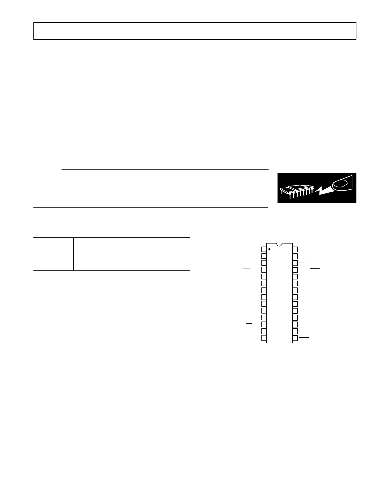
PIN CONFIGURATION
SCLK/DB7
RFS
SDATA/DB11
STBY/DB0
DB8
DB9
/DB10
DGND
DSUBST
DGND
DV
CAL/DB1
UNI
/DB2
DB3
DB4
DD
1
2
3
4
5
AD7721
6
TOP VIEW
(Not to Scale)
7
8
9
10
11
12
13
14
DB6
28
27
RD
26
WR
25
DVAL/SYNC
AGND
24
23
VIN2
VIN1
22
REFIN
21
20
AGND
19
AV
18
CS
17
CLK
16
DRDY
15
SYNC/DB5
DD
REV. A
–5–
 Loading...