a
CMOS Sigma-Delta Modulator
AD7720
FEATURES
12.5 MHz Master Clock Frequency
0 V to +2.5 V or 61.25 V Input Range
Single Bit Output Stream
90 dB Dynamic Range
Power Supplies: AVDD, DVDD: +5 V 6 5%
On-Chip 2.5 V Voltage Reference
28-Lead TSSOP
GENERAL DESCRIPTION
This device is a 7th order sigma-delta modulator that converts
the analog input signal into a high speed 1-bit data stream. The
part operates from a +5 V supply and accepts a differential input
range of 0 V to +2.5 V or ± 1.25 V centered about a commonmode bias. The analog input is continuously sampled by the
analog modulator, eliminating the need for external sample and
hold circuitry. The input information is contained in the output
stream as a density of ones. The original information can be
reconstructed with an appropriate digital filter.
The part provides an accurate on-chip 2.5 V reference. A reference input/output function is provided to allow either the internal reference or an external system reference to be used as the
reference source for the part.
The device is offered in a 28-lead TSSOP package and designed
to operate from –40°C to +85°C.
VIN(+)
VIN(–)
MZERO
GC
BIP
STBY
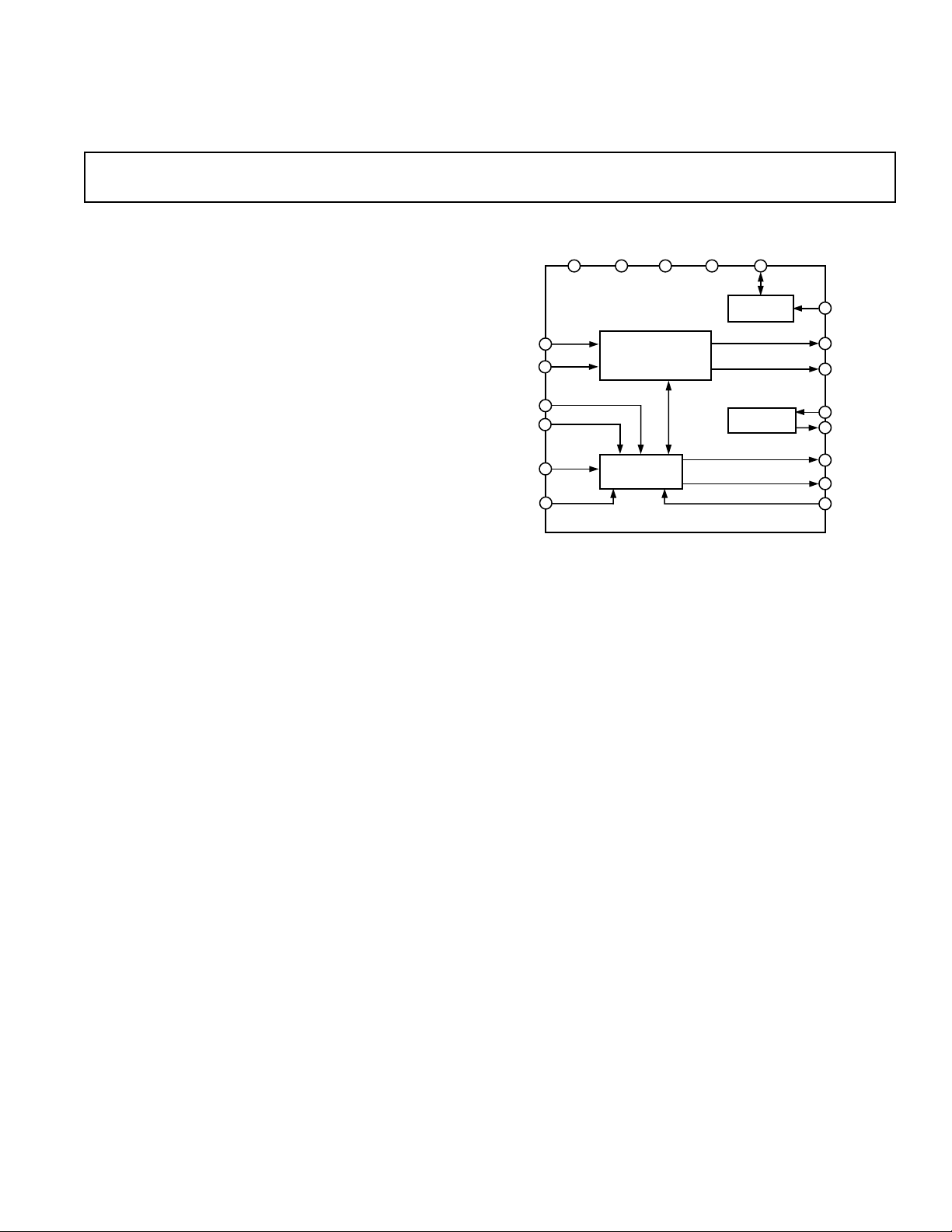
FUNCTIONAL BLOCK DIAGRAM
AVDD AGND DVDD DGND REF1
AD7720
SIGMA-DELTA
MODULATOR
CONTROL
LOGIC
2.5V
REFERENCE
CLOCK
CIRCUITRY
REF2
DATA
SCLK
XTAL1/MCLK
XTAL2
DVAL
RESETO
RESET
REV. 0
Information furnished by Analog Devices is believed to be accurate and
reliable. However, no responsibility is assumed by Analog Devices for its
use, nor for any infringements of patents or other rights of third parties
which may result from its use. No license is granted by implication or
otherwise under any patent or patent rights of Analog Devices.
One Technology Way, P.O. Box 9106, Norwood, MA 02062-9106, U.S.A.
Tel: 781/329-4700 World Wide Web Site: http://www.analog.com
Fax: 781/326-8703 © Analog Devices, Inc., 1997

AD7720–SPECIFICA TIONS
(AVDD = +5 V 6 5%; DVDD = +5 V 6 5%; AGND = DGND = 0 V, f
1
REF2 = +2.5 V; TA = T
MIN
to T
, unless otherwise noted)
MIN
= 12.5 MHz,
MCLK
Parameter B Version Units Test Conditions/Comments
STATIC PERFORMANCE When Tested with Ideal FIR Filter as in Figure 1
Resolution 16 Bits
Differential Nonlinearity ±1 LSB max Guaranteed Monotonic
Integral Nonlinearity ±2 LSB typ
Precalibration Offset Error ±6 mV typ
Precalibration Gain Error
Postcalibration Offset Error
Postcalibration Gain Error
2
3
2, 3
±0.6 % FSR typ
±1.5 mV typ
±0.3 % FSR typ
Offset Error Drift ±1 LSB/°C typ
Gain Error Drift REF2 Is an Ideal Reference, REF1 = AGND
Unipolar Mode ±1 LSB/°C typ
Bipolar Mode ±0.5 LSB/°C typ
ANALOG INPUTS
Signal Input Span (VIN(+) – VIN(–))
Bipolar Mode ±V
Unipolar Mode 0 to V
/2 V max BIP = V
REF2
REF2
V max BIP = V
IH
IL
Maximum Input Voltage AVDD V
Minimum Input Voltage 0 V
Input Sampling Capacitance 2 pF typ
Input Sampling Rate 2 f
MCLK
Differential Input Impedance 109/(8 f
MCLK
MHz
)kΩ typ
REFERENCE INPUTS
REF1 Output Voltage 2.32 to 2.62 V min/max
REF1 Output Voltage Drift 60 ppm/°C typ
REF1 Output Impedance 3 kΩ typ
Reference Buffer Offset Voltage ±12 mV max Offset Between REF1 and REF2
Using Internal Reference
REF2 Output Voltage 2.32 to 2.62 V min/max
REF2 Output Voltage Drift 60 ppm/°C typ
Using External Reference REF1 = AGND
REF2 Input Impedance 10
9
/(16 f
MCLK
)kΩ typ
External Reference Voltage Range 2.32 to 2.62 V min/max Applied to REF1 or REF2
DYNAMIC SPECIFICATIONS
Bipolar Mode BIP = V
Signal to (Noise + Distortion)
Total Harmonic Distortion
4
5
5
90 dB typ Input BW = 0 kHz–90.625 kHz
86/84.5 dB min
–90/–88 dB max Input BW = 0 kHz–90.625 kHz
When Tested with Ideal FIR Filter as in Figure 1
, VCM = 2.5 V, VIN(+) = VIN(–) = 1.25 V p-p
IH
or VIN(–) = 1.25 V, VIN(+) = 0 V to 2.5 V
Spurious Free Dynamic Range –90 dB max Input BW = 0 kHz–90.625 kHz
Unipolar Mode BIP = V
Signal to (Noise + Distortion)
Total Harmonic Distortion
5
5
88 dB typ Input BW = 0 kHz–90.625 kHz
84.5/83 dB min
–89/–87 dB max Input BW = 0 kHz–97.65 kHz
, VIN(–) = 0 V, VIN(+) = 0 V to 2.5 V
IL
Spurious Free Dynamic Range –90 dB max Input BW = 0 kHz–97.65 kHz
Intermodulation Distortion –93 dB typ
AC CMRR 96 dB typ VIN(+) = VIN(–) = 2.5 V p-p, V
= 1.25 V to
CM
3.75 V, 20 kHz
Overall Digital Filter Response See Figure 1 for Characteristics of FIR Filter
0 kHz–90.625 kHz ±0.005 dB max
96.92 kHz –3 dB min
104.6875 kHz to 12.395 MHz 90 dB typ
CLOCK
MCLK Duty Ratio 45 to 55 % max For Specified Operation
V
V
, MCLK High Voltage 4 V min MCLK Uses CMOS Logic
MCLKH
, MCLK Low Voltage 0.4 V max
MCLKL
–2–
REV. 0

Parameter B Version Units Test Conditions/Comments
LOGIC INPUTS
VIH, Input High Voltage 2 V min
V
, Input Low Voltage 0.8 V max
IL
I
, Input Current 10 µA max
INH
CIN, Input Capacitance 10 pF max
LOGIC OUTPUTS
V
, Output High Voltage 2.4 V min |I
OH
VOL, Output Low Voltage 0.4 V max |I
| ≤ 200 µA
OUT
| ≤ 1.6 mA
OUT
POWER SUPPLIES
AVDD 4.75/5.25 V min/V max
DVDD 4.75/5.25 V min/V max
I
(Total for AVDD, DVDD) Digital Inputs Equal to 0 V or DVDD
DD
Active Mode 43 mA max
Standby Mode 25 µA max
NOTES
1
Operating temperature range is as follows: B Version: –40°C to +85°C.
2
Gain Error excludes reference error. The modulator gain is calibrated w.r.t. the voltage on the REF2 pin.
3
Applies after calibration at temperature of interest.
4
Measurement Bandwidth = 0.5 × f
5
TA = +25°C to +85°C/TA = T
Specifications subject to change without notice.
; Input Level = –0.05 dB.
MCLK
to T
MAX
.
MIN
AD7720
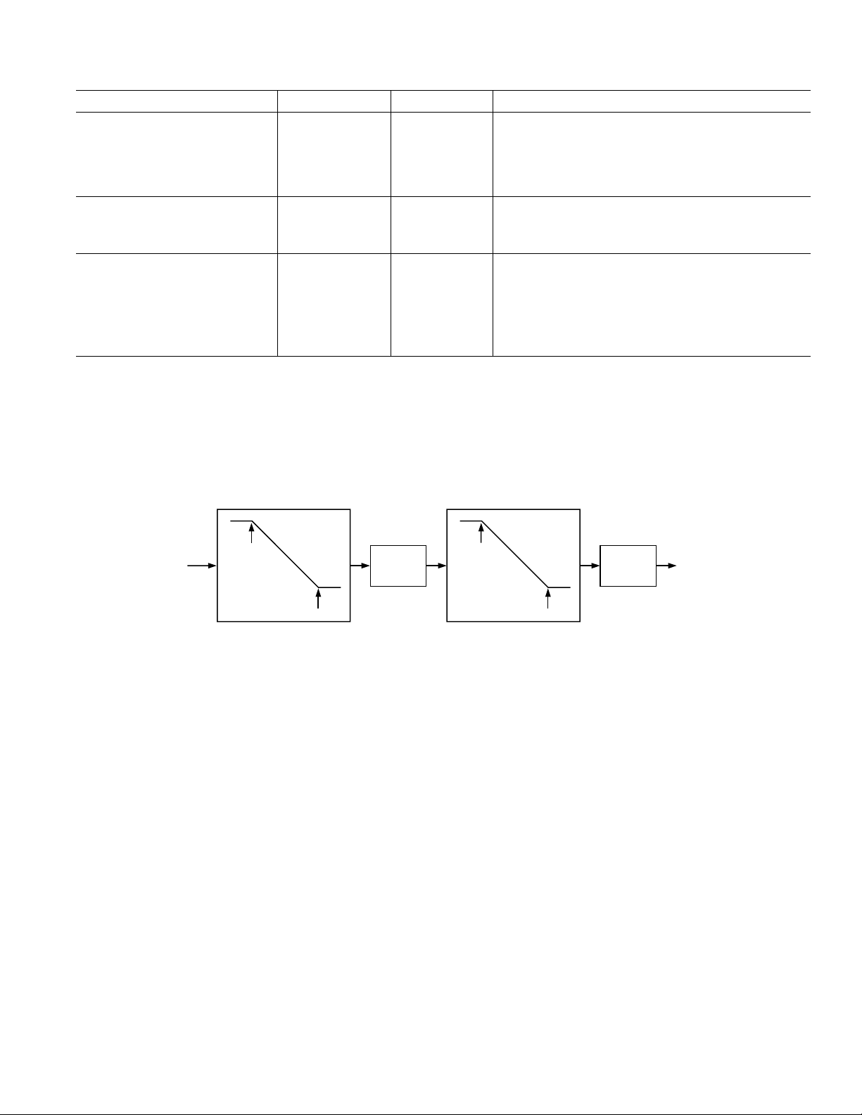
BIT STREAM
90.625kHz
FILTER 1
BANDWIDTH = 90.625 kHz
TRANSITION = 292.969kHz
ATTENUATION = 120dB
COEFFICIENTS = 384
292.969kHz
120dB
DECIMATE
BY 32
90.625kHz
FILTER 2
BANDWIDTH = 90.625 kHz
TRANSITION = 104.687kHz
ATTENUATION = 90dB
COEFFICIENTS = 151
104.687kHz
90dB
DECIMATE
BY 2
16-BIT
OUTPUT
Figure 1. Digital Filter (Consists of 2 FIR Filters). This filter is implemented on the AD7722.
–3–REV. 0

AD7720
TIMING CHARACTERISTICS
Limit at T
(AVDD = +5 V 6 5%; DVDD = +5 V 6 5%; AGND = DGND = 0 V, REF2= +2.5 V unless otherwise noted)
, T
MIN
MAX
Parameter (B Version) Units Conditions/Comments
f
MCLK
100 kHz min Master Clock Frequency
15 MHz max 12.5 MHz for Specified Performance
t
1
t
2
t
3
t
4
t
5
t
6
t
7
NOTE
Guaranteed by design.
67 ns min Master Clock Period
0.45 × t
0.45 × t
MCLK
MCLK
ns min Master Clock Input High Time
ns min Master Clock Input Low Time
15 ns min Data Hold Time After SCLK Rising Edge
10 ns min RESET Pulsewidth
10 ns min RESET Low Time Before MCLK Rising
20 × t
MCLK
OUTPUT
ns max DVAL High Delay after RESET Low
I
OL
1.6mA
PIN
TO
50pF
C
L
I
OH
200 A
+1.6V
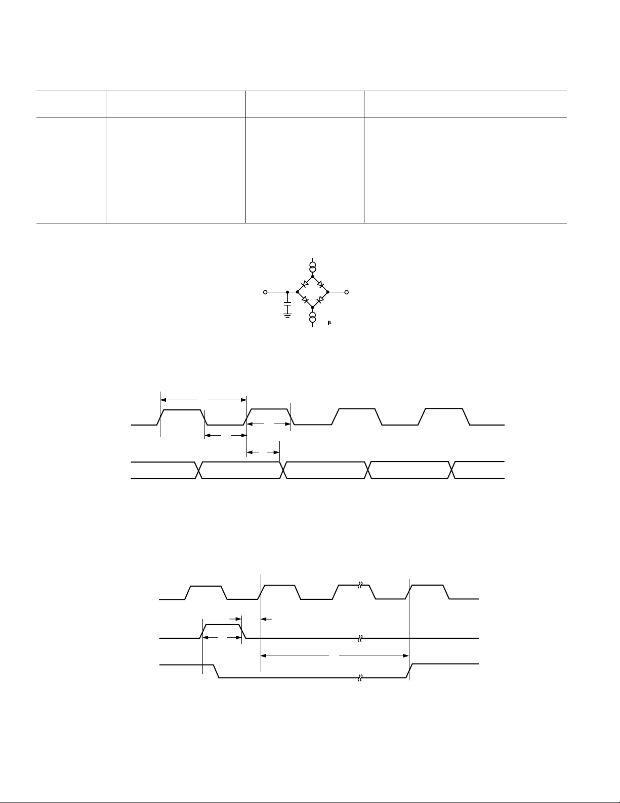
Figure 2. Load Circuit for Access Time and Bus Relinquish Time
SCLK (O)
DATA (O)
NOTE:
O SIGNIFIES AN OUTPUT
MCLK (I)
RESET (I)
DVAL (O)
t
1
t
t
3
2
t
4
Figure 3. Data Timing
t
6
t
5
t
7
NOTE:
I SIGNIFIES AN INPUT
O SIGNIFIES AN OUTPUT
Figure 4. RESET Timing
–4–
REV. 0

AD7720
ABSOLUTE MAXIMUM RATINGS
1
(TA = +25°C unless otherwise noted)
DVDD to DGND . . . . . . . . . . . . . . . . . . . . . . –0.3 V to +7 V
AVDD to AGND . . . . . . . . . . . . . . . . . . . . . . –0.3 V to +7 V
AVDD to DVDD . . . . . . . . . . . . . . . . . . . . –0.3 V to +0.3 V
AGND to DGND . . . . . . . . . . . . . . . . . . . . –0.3 V to +0.3 V
Digital Input Voltage to DGND . . –0.3 V to DVDD + 0.3 V
Analog Input Voltage to AGND . . . –0.3 V to AVDD + 0.3 V
Input Current to Any Pin Except Supplies
2
. . . . . . . ±10 mA
Operating Temperature Range
Industrial (B Version) . . . . . . . . . . . . . . . –40°C to +85°C
Storage Temperature Range . . . . . . . . . . . . –65°C to +150°C
Maximum Junction Temperature . . . . . . . . . . . . . . . +150°C
TSSOP Package
θ
Thermal Impedance . . . . . . . . . . . . . . . . . . . . 120°C/W
JA
Lead Temperature, Soldering
Vapor Phase (60 sec) . . . . . . . . . . . . . . . . . . . . . +215°C
Infrared (15 sec) . . . . . . . . . . . . . . . . . . . . . . . . . +220°C
NOTES
1
Stresses above those listed under Absolute Maximum Ratings may cause perma-
nent damage to the device. This is a stress rating only; functional operation of the
device at these or any other conditions above those listed in the operational
sections of this specification is not implied. Exposure to absolute maximum rating
conditions for extended periods may affect device reliability.
2
Transient currents of up to 100 mA will not cause SCR latchup.
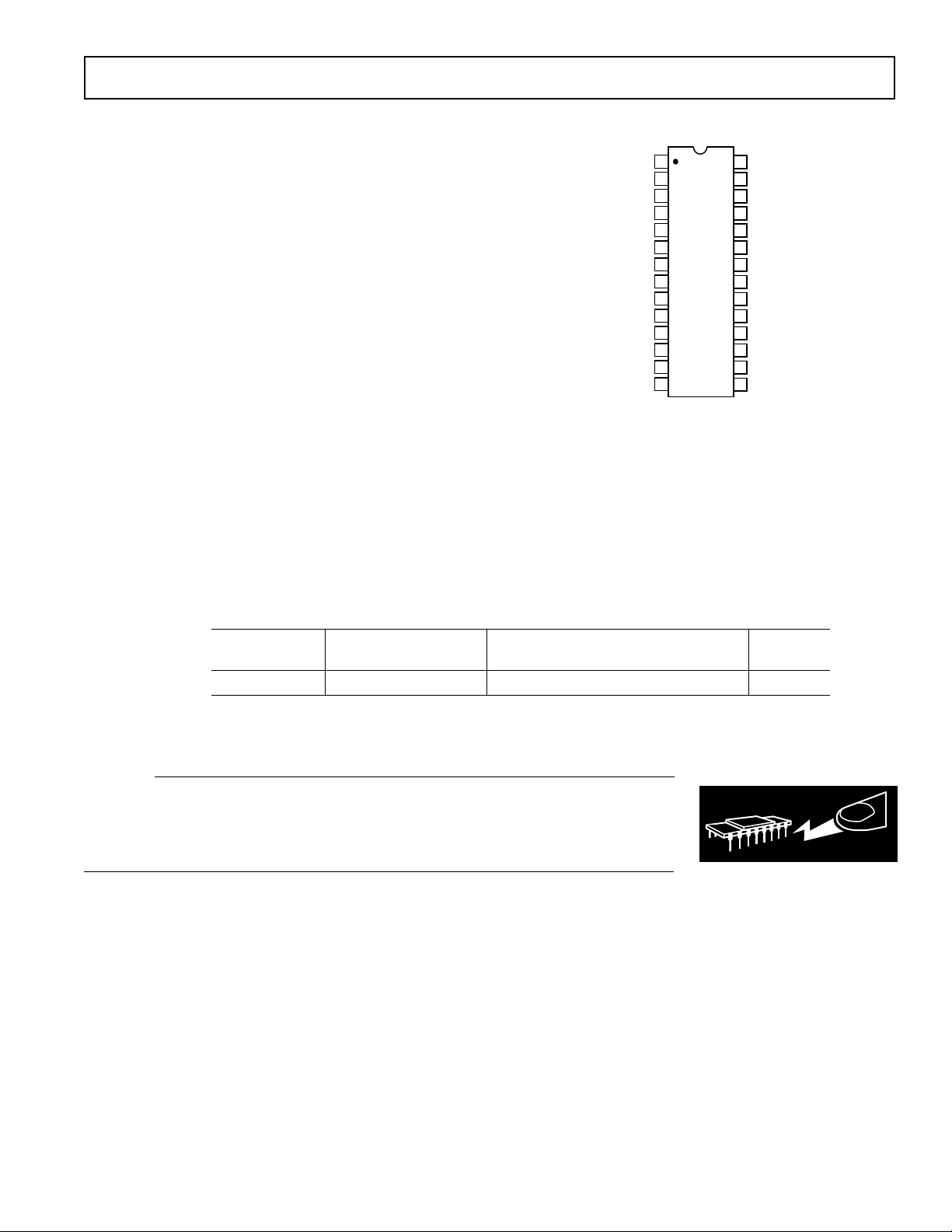
PIN CONFIGURATION
REF2
AGND
NC
STBY
DVAL
DGND
GC
BIP
MZERO
DATA
SCLK
RESETO
NC
AGND
1
2
3
4
5
6
AD7720
7
TOP VIEW
(Not to Scale)
8
9
10
11
12
13
14
NC = NO CONNECT
28
AVDD
27
REF1
26
AGND
25
AVDD
24
AGND
VIN(+)
23
22
RESET
21
VIN(–)
20
AGND
19
DVDD
18
AGND
17
XTAL2
16
XTAL1/MCLK
15
DGND
ORDERING GUIDE
Temperature Package Package
Model Range Description Option
AD7720BRU –40°C to +85°C 28-Lead Thin Shrink Small Outline RU-28
CAUTION
ESD (electrostatic discharge) sensitive device. Electrostatic charges as high as 4000 V readily
accumulate on the human body and test equipment and can discharge without detection.
Although the AD7720 features proprietary ESD protection circuitry, permanent damage may
occur on devices subjected to high energy electrostatic discharges. Therefore, proper ESD
precautions are recommended to avoid performance degradation or loss of functionality.
WARNING!
ESD SENSITIVE DEVICE
–5–REV. 0
 Loading...