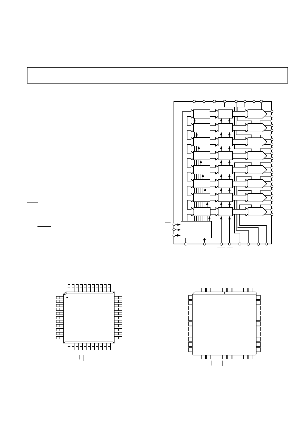
FUNCTIONAL BLOCK DIAGRAM
R B
R F
DAC A
DAC A
LATCH
INPUT
LATCH A
INPUT
LATCH B
INPUT
LATCH C
INPUT
LATCH D
INPUT
LATCH E
INPUT
LATCH F
INPUT
LATCH G
DAC B
LATCH
DAC C
LATCH
DAC D
LATCH
DAC E
LATCH
DAC F
LATCH
DAC G
LATCH
DAC B
DAC C
DAC D
DAC E
DAC F
DAC G
V B
REF
V D
REF
R G
FB
V G
REF
V F
REF
V E
REF
FB
FB
R E
R D
R C
FB
FB
R A
FBREF
V AV C
REF
V
DD
DGND
LDAC
CLR
AD7568
12
12
12
12
12
12
12
12
12
12
12
12
12
12
V H
REF
A0
CONTROL LOGIC
+
INPUT SHIFT
REGISTER
CLKIN
SDIN
SDOUT
INPUT
LATCH H
DAC H
LATCH
DAC H
R H
FB
12
12
FSIN
I A
I A
I B
I B
I C
I D
I C
I D
I E
I F
I E
I F
I G
I H
I G
I H
AGND
12
OUT1
OUT2
OUT1
OUT2
OUT1
OUT2
FB
OUT1
OUT2
OUT1
OUT2
OUT1
OUT2
OUT1
OUT2
OUT1
OUT2
a
LC2MOS
Octal 12-Bit DAC
AD7568
One Technology Way, P.O. Box 9106, Norwood, MA 02062-9106, U.S.A.
Tel: 617/329-4700 Fax: 617/326-8703
FEATURES
Eight 12-Bit DACs in One Package
4-Quadrant Multiplication
Separate References
Single +5 V Supply
Low Power: 1 mW
Versatile Serial Interface
Simultaneous Update Capability
Reset Function
44-Pin PQFP and PLCC
APPLICATIONS
Process Control
Automatic Test Equipment
General Purpose Instrumentation
PIN CONFIGURATIONS
Plastic Quad Flatpack Plastic Leaded Chip Carrier
AD7568
TOP VIEW
(Not to Scale)
121314
151617
181920
21
22
4443424140393837363534
33
32
31
30
29
28
27
26
25
24
23
1
2
3
4
5
6
7
8
9
10
11
PIN 1 IDENTIFIER
NC
V B
REF
V D
REF
R G
FB
V G
REF
V F
REF
V E
REF
FB
R F
FB
R E
FB
R D
R C
FB
FB
R B
R A
FB
REF
V A
V C
REF
VDDDGND
LDAC
CLR
V H
REF
A0
CLKIN
SDIN
SDOUT
R H
FB
FSIN
I C
I F
I E
I H
AGND
NC
NC = NO CONNECT
OUT2
I E
OUT1
I D
OUT1
I D
OUT2
OUT1
I C
OUT2
I B
OUT1
I B
OUT2
OUT1
I H
OUT2
I A
OUT2
I A
OUT1
OUT1
I F
OUT2
I G
OUT1
I G
OUT2
AD7568 PQFP
TOP VIEW
Not to Scale
NC = NO CONNECT
NC
V
REF
C
V
REF
B
R
FB
B
I
OUT1
B
I
OUT1
C
NC
V
REF
F
V
REF
G
R
FB
G
R
FB
F
I
OUT2
F
I
OUT2
E
I
OUT1
E
V
DD
DGND
AGND
R
FB
E
I
OUT1
H
I
OUT2
H
LDAC
FSIN
SDIN
SDOUT
CLR
V
REF
E
R
FB
D
I
OUT1
D
A0
I
OUT2
A
I
OUT1
A
CLKIN
V
REF
D
V
REF
A
R
FB
A
I
OUT2
B
I
OUT2
G
V
REF
H
R
FB
H
I
OUT1
G
4412645
21 24
23
22182019
39
38
35
34
33
37
36
3
7
8
11
12
13
9
10
404142
25 28
27
26
43
31
30
29
32
15
16
17
14
TOP VIEW
(Not to Scale)
AD7568 PLCC
I
OUT2
D
I
OUT2
C
R
FB
C
I
OUT1
F
GENERAL DESCRIPTION
The AD7568 contains eight 12-bit DACs in one monolithic device. The DACs are standard current output with separate V
REF
,
I
OUT1
, I
OUT2
and RFB terminals.
The AD7568 is a serial input device. Data is loaded using
FSIN, CLKIN and SDIN. One address pin, A0, sets up a device address, and this feature may be used to simplify device
loading in a multi-DAC environment.
All DACs can be simultaneously updated using the asynchronous
LDAC input and they can be cleared by asserting the
asynchronous
CLR input.
The AD7568 is housed in a space-saving 44-pin plastic quad
flatpack and 44-lead PLCC.
REV. B
Information furnished by Analog Devices is believed to be accurate and
reliable. However, no responsibility is assumed by Analog Devices for its
use, nor for any infringements of patents or other rights of third parties
which may result from its use. No license is granted by implication or
otherwise under any patent or patent rights of Analog Devices.

REV. B
–2–
AD7568–SPECIFICA TIONS
1
Parameter AD7568B
2
Units Test Conditions/Comments
ACCURACY
Resolution 12 Bits 1 LSB = V
REF
/212 = 1.22 mV when V
REF
= 5 V
Relative Accuracy ±0.5 LSB max
Differential Nonlinearity ± 0.9 LSB max All Grades Guaranteed Monotonic over Temperature
Gain Error
+25°C ±4 LSBs max
T
MIN
to T
MAX
±5 LSBs max
Gain Temperature Coefficient 2 ppm FSR/°C typ
5 ppm FSR/°C max
Output Leakage Current
I
OUT1
@ +25°C 10 nA max See Terminology Section
T
MIN
to T
MAX
200 nA max
REFERENCE INPUT
Input Resistance 5 kΩ min Typical Input Resistance = 7 kΩ
9kΩ max
Ladder Resistance Mismatch 2 % max Typically 0.6%
DIGITAL INPUTS
V
INH
, Input High Voltage 2.4 V min
V
INL
, Input Low Voltage 0.8 V max
I
INH
, Input Current ±1 µA max
CIN, Input Capacitance 10 pF max
POWER REQUIREMENTS
V
DD
Range 4.75/5.25 V min/V max
Power Supply Sensitivity
∆Gain/∆V
DD
–75 dB typ
I
DD
300 µA max V
INH
= 4.0 V min, V
INL
= 0.4 V max
3.5 mA max V
INH
= 2.4 V min, V
INL
= 0.8 V max
AC PERFORMANCE CHARACTERISTICS
Parameter AD7568B
2
Units Test Conditions/Comments
DYNAMIC PERFORMANCE
Output Voltage Settling Time 500 ns typ To 0.01% of Full-Scale Range. DAC Latch Alternately
Loaded with All 0s and All 1s.
Digital to Analog Glitch Impulse 40 nV–s typ Measured with V
REF
= 0 V. DAC Register Alternately
Loaded with All 0s and All 1s.
Multiplying Feedthrough Error –66 dB max V
REF
= 20 V pk-pk, 10 kHz Sine Wave. DAC Latch
Loaded with All 0s.
Output Capacitance 60 pF max All 1s Loaded to DAC.
30 pF max All 0s Loaded to DAC.
Channel-to-Channel Isolation –76 dB typ Feedthrough from Any One Reference to the Others
with 20 V pk-pk, 10 kHz Sine Wave Applied.
Digital Crosstalk 40 nV–s typ Effect of all 0s to all 1s Code Transition on
Nonselected DACs.
Digital Feedthrough 40 nV–s typ Feedthrough to Any DAC Output with
FSIN High
and Square Wave Applied to SDIN and SCLK.
Total Harmonic Distortion –83 dB typ V
REF
= 6 V rms, 1 kHz Sine Wave.
Output Noise Spectral Density
@ 1 kHz 20 nV/√
Hz All 1s Loaded to the DAC. V
REF
= 0 V. Output Op
Amp is AD OP07.
NOTES
1
Temperature range as follows: B Version: –40°C to +85°C.
2
All specifications also apply for V
REF
= +10 V, except relative accuracy which degrades to ±1 LSB.
Specifications subject to change without notice.
(VDD = +4.75 V to +5.25 V; I
OUT1
= I
OUT2
= O V; V
REF
= +5 V; TA = T
MIN
to T
MAX
,
unless otherwise noted)
(These characteristics are included for Design Guidance and are not subject
to test. DAC output op amp is AD843.)

AD7568
REV. B
–3–
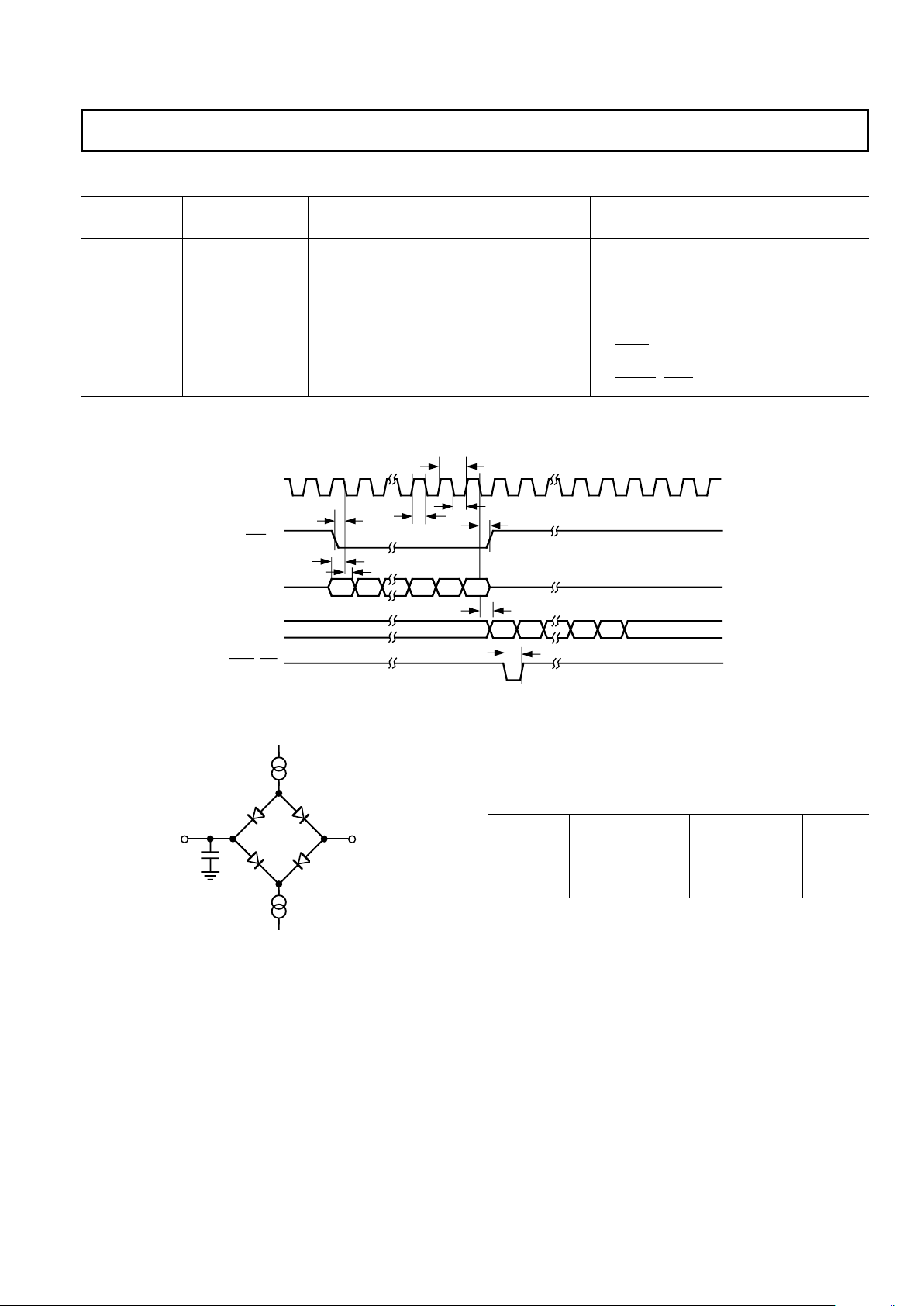
TIMING SPECIFICATIONS
Limit at Limit at
Parameter TA = +258CT
A
= –408C to +858C Units Description
t
1
100 100 ns min CLKIN Cycle Time
t
2
40 40 ns min CLKIN High Time
t
3
40 40 ns min CLKIN Low Time
t
4
30 30 ns min FSIN Setup Time
t
5
30 30 ns min Data Setup Time
t
6
5 5 ns min Data Hold Time
t
7
90 90 ns min FSIN Hold Time
t
8
2
70 70 ns max SDOUT Valid After CLKIN Falling Edge
t
9
40 40 ns min LDAC, CLR Pulse Width
NOTES
1
Sample tested at +25°C to ensure compliance. All input signals are specified with tr = tf = 5 ns (10% to 90% of 5 V) and timed from a voltage level of 1.6 V.
2
t8 is measured with the load circuit of Figure 2 and defined as the time required for the output to cross 0.8 V or 2.4 V.
CLKIN (I)
SDIN (I)
SDOUT (O)
DB15 DB0
DB15
DB0
FSIN (I)
LDAC, CLR
t
1
t
4
t
7
t
2
t
3
t
6
t
5
t
8
t
9
NOTES
1. AO IS HARDWIRED HIGH OR LOW.
Figure 1. Timing Diagram
(VDD = +5 V 6 5%; I
OUT1
= I
OUT2
= 0 V; TA = T
MIN
to T
MAX
, unless otherwise noted)
1.6mA I
OL
+2.1V
I
OH
200µA
C
L
50pF
TO OUTPUT
PIN
Figure 2. Load Circuit for Digital Output
Timing Specifications
ORDERING GUIDE
Temperature Linearity Package
Model Range Error (LSBs) Option*
AD7568BS –40°C to +85°C ±0.5 S-44
AD7568BP –40°C to +85°C ±0.5 P-44A
*S = Plastic Quad Flatpack (PQFP), P = Plastic Leaded Chip Carrier (PLCC).

AD7568
REV. B
–4–
ABSOLUTE MAXIMUM RATINGS
1
(TA = +25°C unless otherwise noted)
VDD to DGND . . . . . . . . . . . . . . . . . . . . . . . . . –0.3 V to +6 V
I
OUT1
to DGND . . . . . . . . . . . . . . . . . . . –0.3 V to VDD +0.3 V
I
OUT2
to DGND . . . . . . . . . . . . . . . . . . . –0.3 V to VDD +0.3 V
Digital Input Voltage to DGND . . . . . . –0.3 V to V
DD
+0.3 V
V
RFB
, V
REF
to DGND . . . . . . . . . . . . . . . . . . . . . . . . . . ±15 V
Input Current to Any Pin Except Supplies
2
. . . . . . . . ±10 mA
Operating Temperature Range
Commercial Plastic (B Versions) . . . . . . . . –40°C to +85°C
Storage Temperature Range . . . . . . . . . . . . –65°C to +150°C
Lead Temperature (Soldering, 10 secs) . . . . . . . . . . . +300°C
Power Dissipation (Any Package) to +75°C . . . . . . . . 250 mW
Derates above +75°C by . . . . . . . . . . . . . . . . . . . . 10 mW/°C
NOTES
1
Stresses above those listed under “Absolute Maximum Ratings” may cause
permanent damage to the device. This is a stress rating only and functional
operation of the device at these or any other conditions above those listed in the
operational sections of this specification is not implied. Exposure to absolute
maximum rating conditions for extended periods may affect device reliability.
2
Transient currents of up to 100 mA will not cause SCR latch-up.
WARNING!
ESD SENSITIVE DEVICE
CAUTION
ESD (electrostatic discharge) sensitive device. Electrostatic charges as high as 4000 V readily
accumulate on the human body and test equipment and can discharge without detection.
Although the AD7568 features proprietary ESD protection circuitry, permanent damage may
occur on devices subjected to high energy electrostatic discharges. Therefore, proper ESD
precautions are recommended to avoid performance degradation or loss of functionality.
PIN DESCRIPTION
Pin Description
V
DD
Positive power supply. This is +5 V ± 5%.
DGND Digital Ground.
AGND Analog Ground.
V
REF
A – V
REF
H DAC reference inputs.
R
FB
A – RFBH DAC feedback resistor pins.
I
OUT
A – I
OUT
H DAC current output terminals.
AGND This pin connects to the back gates of the current steering switches. It should be connected to the signal ground
of the system.
CLKIN Clock Input. Data is clocked into the input shift register on the falling edges of CLKIN.
FSIN Level-triggered control input (active low). This is the frame synchronization signal for the input data. When
FSIN goes low, it enables the input shift register, and data is transferred on the falling edges of CLKIN. If the
address bit is valid, the 12-bit DAC data is transferred to the appropriate input latch on the sixteenth falling
edge after
FSIN goes low.
SDIN Serial data input. The device accepts a 16-bit word. The first bit (DB15) is the DAC MSB, with the remaining
bits following. Next comes the device address bit, A0. If this does not correspond to the logic level on pin A0,
the data is ignored. Finally come the three DAC select bits. These determine which DAC in the device is se-
lected for loading.
SDOUT This shift register output allows multiple devices to be connected in a daisy chain configuration.
A0 Device address pin. This input gives the device an address. If DB3 of the serial input stream does not corre-
spond to this, the data which follows is ignored and not loaded to any input latch. However it will appear at
SDOUT irrespective of this.
LDAC Asynchronous LDAC input. When this input is taken low, all DAC latches are simultaneously updated with the
contents of the input latches.
CLR Asynchronous CLR input. When this input is taken low, all DAC latch outputs go to zero.
 Loading...