Analog Devices AD7564 Datasheet

LC2MOS
a
+3.3 V/+5 V, Low Power, Quad 12-Bit DAC
FEATURES
Four 12-Bit DACs in One Package
4-Quadrant Multiplication
Separate References
Single Supply Operation
Guaranteed Specifications with +3.3 V/+5 V Supply
Low Power
Versatile Serial Interface
Simultaneous Update Capability
Reset Function
28-Pin SOIC, SSOP and DIP Packages
APPLICATIONS
Process Control
Portable Instrumentation
General Purpose Test Equipment
FSIN
CLKIN
SDIN
AD7564
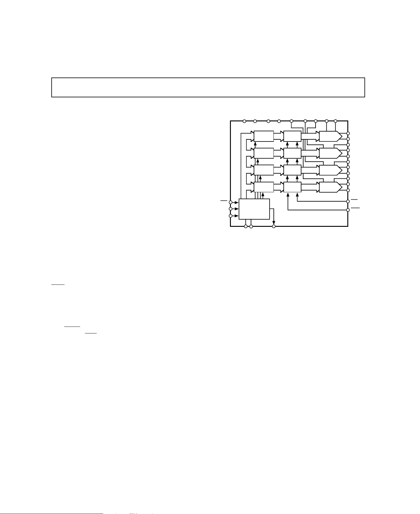
FUNCTIONAL BLOCK DIAGRAM
VDDDGND
AGND
NC
INPUT
LATCH A
INPUT
LATCH B
INPUT
LATCH C
INPUT
LATCH D
12
CONTROL LOGIC
+
INPUT SHIFT
REGISTER
A0 A1
SDOUT
V D
REF
DAC A
12
LATCH
DAC B
12
LATCH
DAC C
12
LATCH
DAC D
12
LATCH
V C
REF
12
12
12
12
V B
REF
AD7564
V A
REF
DAC A
DAC B
DAC C
DAC D
R A
FB
I A
OUT1
I A
OUT2
R B
FB
I B
OUT1
I B
OUT2
R C
FB
I C
OUT1
I C
OUT2
R D
FB
I D
OUT1
I D
OUT2
CLR
LDAC
GENERAL DESCRIPTION
The AD7564 contains four 12-bit DACs in one monolithic
device. The DACs are standard current output with separate
, I
, I
V
REF
OUT1
and RFB terminals. These DACs operate from
OUT2
a single +3.3 V to +5 V supply.
The AD7564 is a serial input device. Data is loaded using
FSIN, CLKIN and SDIN. Two address pins A0 and A1 set up
a device address, and this feature may be used to simplify device
loading in a multi-DAC environment. Alternatively, A0 and A1
can be ignored and the serial out capability used to configure a
daisy-chained system.
All DACs can be simultaneously updated using the asynchro-
LDAC input, and they can be cleared by asserting the
nous
asynchronous
CLR input.
The device is packaged in 28-pin SOIC, SSOP and DIP
packages.
PRODUCT HIGHLIGHTS
1. The AD7564 contains four 12-bit current output DACs with
separate V
REF
inputs.
2. The AD7564 can be operated from a single +3.3 V to +5 V
supply.
3. Simultaneous update capability and reset function are
available.
4. The AD7564 features a fast, versatile serial interface compatible with modern 3 V and 5 V microprocessors and
microcomputers.
5. Low power, 50 µW at 5 V and 33 µW at 3.3 V.
REV. A
Information furnished by Analog Devices is believed to be accurate and
reliable. However, no responsibility is assumed by Analog Devices for its
use, nor for any infringements of patents or other rights of third parties
which may result from its use. No license is granted by implication or
otherwise under any patent or patent rights of Analog Devices.
One Technology Way, P.O. Box 9106, Norwood. MA 02062-9106, U.S.A.
Tel: 617/329-4700 Fax: 617/326-8703

AD7564–SPECIFICATIONS
(V
= +4.75 V to +5.25 V; I
Normal Mode
DD
unless otherwise noted)
Parameter B Grade
ACCURACY
Resolution 12 Bits 1 LSB = V
Relative Accuracy ±0.5 LSB max
Differential Nonlinearity ± 0.5 LSB max All Grades Guaranteed Monotonic Over Temperature
Gain Error
+25°C ±4 LSBs max
to T
T
MIN
MAX
Gain Temperature Coefficient
±5 LSBs max
2
2 ppm FSR/°C typ
5 ppm FSR/°C max
Output Leakage Current
I
OUT1
@ +25°C 10 nA max
T
MIN
to T
MAX
50 nA max
REFERENCE INPUT
Input Resistance 6 kΩ min Typical Input Resistance = 9.5 kΩ
13 kΩ max
Ladder Resistance Mismatch 2 % max Typically 0.6%
DIGITAL INPUTS
, Input High Voltage 2.4 V min
V
INH
, Input Low Voltage 0.8 V max
V
INL
, Input Current ±1 µA max
I
INH
CIN, Input Capacitance
2
10 pF max
OUT1
1
A to I
OUT1
D = I
OUT2
A = I
D = AGND = 0 V; V
OUT2
REF
Units Test Conditions/Comments
/212 = 2.44 mV when V
REF
= +10 V; TA = T
MIN
to T
MAX
REF
,
= 10 V
DIGITAL OUTPUT (SDOUT)
Output Low Voltage (V
) 0.4 V max Load Circuit as in Figure 2.
OL
Output High Voltage (VOH) 4.0 V min
POWER REQUIREMENTS
Range 4.75/5.25 V min/V max Part Functions from 3.3 V to 5.25 V
V
DD
Power Supply Rejection
∆Gain/∆V
I
DD
DD
2
–75 dB typ
10 µA max V
= VDD, V
INH
INL
= 0 V
At Input Levels of 0.8 V and 2.4 V, I
Typically 2 mA.
NOTES
1
Temperature range is as follows: B Version: –40°C to +85°C.
2
Not production tested. Guaranteed by characterization at initial product release.
Specifications subject to change without notice.
DD
is
–2–
REV. A

(V
Biased Mode
= +3 V to +5.5 V; V
DD
1
, unless otherwise noted)
T
MAX
IOUT1
= V
= 1.23 V; AGND = 0 V; V
IOUT2
Parameter A Grade
= 0 V to 2.45 V; TA = T
REF
2
Units Test Conditions/Comments
MIN
to
AD7564
ACCURACY
Resolution 12 Bits 1 LSB = (V
V
IOUT2
– V
IOUT2
= 1.23 V and V
REF
)/2
REF
12
= 0 V
= 300 µV when
Relative Accuracy ±1 LSB max
Differential Nonlinearity ±0.9 LSB max All Grades Guaranteed Monotonic Over
Temperature
Gain Error
+25°C ±4 LSBs max
to T
T
MIN
Gain Temperature Coefficient
MAX
3
±5 LSBs max
2 ppm FSR/°C typ
5 ppm FSR/°C max
Output Leakage Current See Terminology Section
I
OUT1
@ +25°C 10 nA max
T
MIN
to T
MAX
50 nA max
Input Resistance
@ I
Pins 6 kΩ min This Varies with DAC Input Code
OUT2
DIGITAL INPUTS
, Input High Voltage @ VDD = +5 V 2.4 V min
V
INH
, Input High Voltage @ VDD = +3.3 V 2.1 V min
V
INH
, Input Low Voltage @ VDD = +5 V 0.8 V max
V
INL
, Input Low Voltage @ VDD = +3.3 V 0.6 V max
V
INL
, Input Current ±1 µA max
I
INH
CIN, Input Capacitance
3
10 pF max
DIGITAL OUTPUT (SDOUT) Load Circuit as in Figure 2.
Output Low Voltage (V
Output Low Voltage (V
Output High Voltage (V
Output High Voltage (VOH)V
) 0.4 V max VDD = +5 V
OL
) 0.2 V max VDD = +3.3 V
OL
) 4.0 V min VDD = +5 V
OH
– 0.2 V min VDD = +3.3 V
DD
POWER REQUIREMENTS
Range 3/5.5 V min/V max
V
DD
Power Supply Sensitivity
∆Gain/∆V
I
DD
DD
3
–75 dB typ
10 µA max V
= VDD – 0.1 V min, V
INH
= 0.1 V max;
INL
SDOUT Open Circuit
is typically 2 mA with VDD = +5 V,
I
DD
= 2.4 V min, V
V
INH
= 0.8 V max;
INL
SDOUT Open Circuit
NOTES
1
These specifications apply with the devices biased up at 1.23 V for single supply applications. The model numbering reflects this by means of a "-B" suffix
(for example: AD7564AR-B). Figure 19 is an example of Biased Mode Operation.
2
Temperature ranges is as follows: A Version: –40°C to +85°C.
3
Not production tested. Guaranteed by characterization at initial product release.
Specifications subject to change without notice.
REV. A
–3–

AD7564
AC Performance Characteristics
(VDD = +4.75 V to +5.25 V; V
= T
to T
, unless otherwise noted. These characteristics are included for Design Guidance and are
MAX
Normal Mode
AD843; T
A
MIN
not subject to test.)
Parameter B Grade Units Test Conditions/Comments
DYNAMIC PERFORMANCE
Output Voltage Settling Time 550 ns typ To 0.01% of Full-Scale Range. DAC Latch Alternately Loaded
Digital-to-Analog Glitch Impulse 35 nV-s typ Measured with V
Multiplying Feedthrough Error –70 dB max V
Output Capacitance 60 pF max All 1s Loaded to DAC
30 pF max All 0s Loaded to DAC
Channel-to-Channel Isolation –76 dB typ Feedthrough from Any One Reference to the Others with
Digital Crosstalk 5 nV-s typ Effect of All 0s to All 1s Code Transition on Nonselected DACs
Digital Feedthrough 5 nV-s typ Feedthrough to Any DAC Output with
Total Harmonic Distortion –83 dB typ V
Output Noise Spectral Density
@ 1 kHz 30 nV/√
= V
IOUT1
= AGND = 0 V. V
IOUT2
= 6 V rms, 1 kHz sine wave; DAC output op amp is
REF
with All 0s and All 1s
with All 0s and All 1s
REF
= 20 V p-p, 10 kHz Sine Wave. DAC Latch Loaded
REF
with All 0s
20 V p-p, 10 kHz Sine Wave Applied
Wave Applied to SDIN and SCLK
= 6 V rms, 1 kHz Sine Wave
REF
Hz typ All 1s Loaded to the DAC. V
ADOP07
= 0 V. DAC Register Alternately Loaded
FSIN High and Square
= 0 V. Output Op Amp Is
REF
AC Performance Characteristics
(VDD = +3 V to +5.5 V; V
output op amp is AD820; T
Biased Mode
Guidance and are not subject to test.)
Parameter A Grade Units Test Conditions/Comments
DYNAMIC PERFORMANCE
Output Voltage Settling Time 3.5 µs typ To 0.01% of Full-Scale Range. V
Digital to Analog Glitch Impulse 35 nV-s typ Measured with V
Multiplying Feedthrough Error –70 dB max DAC Latch Loaded with all 0s.
Output Capacitance 100 pF max All 1s Loaded to DAC
40 pF max All 0s Loaded to DAC
Digital Feedthrough 5 nV-s typ Feedthrough to Any DAC Output with FSIN HIGH and a Square
Total Harmonic Distortion –76 dB typ
Output Noise Spectral Density
@ 1 kHz 20 nV/√Hz typ All 1s Loaded to DAC. V
IOUT1
= T
A
= V
= 1.23 V; AGND = 0 V. V
IOUT2
to T
MIN
, unless otherwise noted. These characteristics are included for Design
MAX
= 1 kHz, 2.45 V p-p, sine wave biased at 1.23 V; DAC
REF
= 0 V. DAC Latch Alter-
REF
nately Loaded with all 0s and all 1s.
= 0 V and V
IOUT2
REF
nately Loaded with all 0s and all 1s.
Wave Applied to SDIN and CLKIN
= 0 V; V
IOUT2
= 0 V. DAC Register Alter-
= 0 V
REF
–4–
REV. A

AD7564
Timing Specifications
1
(TA = T
MIN
to T
unless otherwise noted)
MAX
Limit at Limit at
Parameter V
t
1
t
2
t
3
t
4
t
5
t
6
t
7
2
t
8
t
9
NOTES
1
Not production tested. Guaranteed by characterization at initial product release. All input signals are specified with tr = tf = 5 ns (10% to 90% of VDD) and timed
from a voltage level of 1.6 V for a V
2
t8 is measured with the load circuit of Figure 2 and defined as the time required for the output to cross 0.8 V or 2.4 V with a V
of 3.3 V.
CLKIN(I)
FSIN(I)
SDIN(I)
= +3 V to +3.6 V VDD = +4.75 V to +5.25 V Units Description
DD
180 100 ns min CLKIN Cycle Time
80 40 ns min CLKIN High Time
80 40 ns min CLKIN Low Time
50 30 ns min FSIN Setup Time
50 30 ns min Data Setup Time
10 5 ns min Data Hold Time
125 90 ns min FSIN Hold Time
100 70 ns max SDOUT Valid After CLKIN Falling Edge
80 40 ns min LDAC, CLR Pulse Width
of 5 V and from a voltage level 1.35 V for a VDD of 3.3 V.
DD
t
5
DB15
t
1
t
t
t
4
t
6
2
3
DB0
t
7
of 5 V and 0.6 V or 2.1 V for a V
DD
3
DD
SDOUT(O)
LDAC, CLR
t
8
DB15
t
9
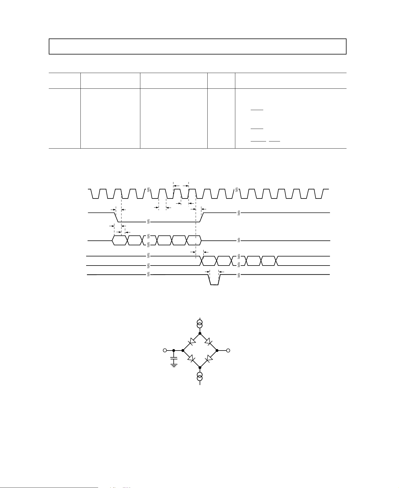
Figure 1. Timing Diagram
I
OL
+1.6V
I
OH
TO OUTPUT
PIN
C
L
50pF
1.6mA
200µA
Figure 2. Load Circuit for Digital Output Timing Specifications
DB0
REV. A
–5–
 Loading...