Analog Devices AD7545AUQ, AD7545ATQ, AD7545ALP, AD7545AKP, AD7545ACE Datasheet
...
CMOS 12-Bit
a
FEATURES
Improved Version of AD7545
Fast Interface Timing
All Grades 12-Bit Accurate
20-Lead DIP and Surface Mount Packages
Low Cost
GENERAL DESCRIPTION
The AD7545A, a 12-bit CMOS multiplying DAC with internal
data latches, is an improved version of the industry standard
AD7545. This new design features a WR pulse width of 100 ns,
which allows interfacing to a much wider range of fast 8-bit and
16-bit microprocessors. It is loaded by a single 12-bit-wide word
under the control of the CS and WR inputs; tying these control
inputs low makes the input latches transparent, allowing unbuffered operation of the DAC.
Buffered Multiplying DAC
AD7545A
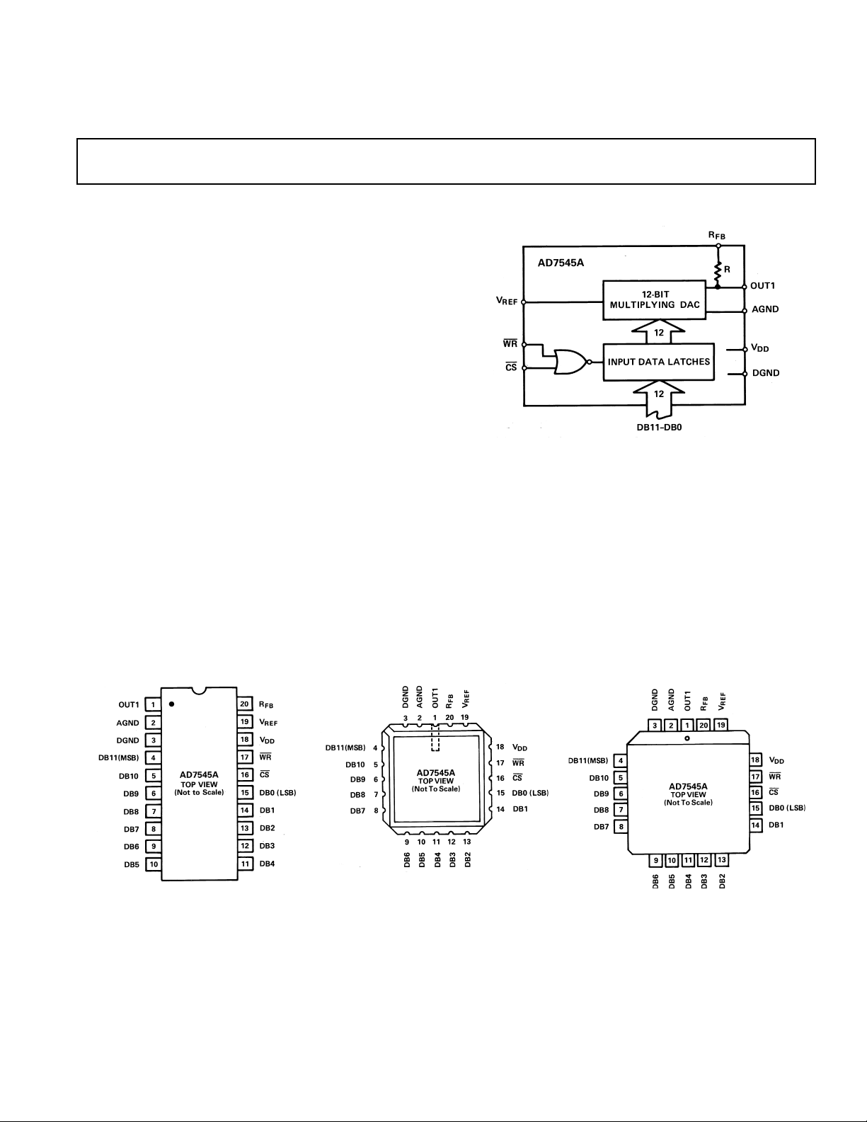
FUNCTIONAL BLOCK DIAGRAM
PIN CONFIGURATIONS
DIP/SOIC LCCC PLCC
REV. C
Information furnished by Analog Devices is believed to be accurate and
reliable. However, no responsibility is assumed by Analog Devices for its
use, nor for any infringements of patents or other rights of third parties
which may result from its use. No license is granted by implication or
otherwise under any patent or patent rights of Analog Devices.
One Technology Way, P.O. Box 9106, Norwood, MA 02062-9106, U.S.A.
Tel: 781/329-4700 World Wide Web Site: http://www.analog.com
Fax: 781/326-8703 © Analog Devices, Inc., 2000

AD7545A–SPECIFICATIONS
= ⴞ10 V, V
REF
= O V, AGND = DGND unless otherwise noted)
OUT1
(V
VDD = +5 V VDD = +15 V
Parameter Version TA = + 25ⴗCT
Limits Limits
MIN–TMAX
1
TA = + 25ⴗCT
MIN–TMAX
1
Units Test Conditions/Comments
STATIC PERFORMANCE
Resolution All 12 12 12 12 Bits
Relative Accuracy K, B, T ±1/2 ± 1/2 ±1/2 ±1/2 LSB max
L, C, U ±1/2 ±1/2 ±1/2 ± 1/2 LSB max Endpoint Measurement
Differential Nonlinearity All ±1 ±1 ±1 ±1 LSB max All Grades Guaranteed 12-Bit
Monotonic Over Temperature
Gain Error K, B, T ±3 ± 4 ±3 ±4 LSB max Measured Using Internal R
L, C, U ±1 ±2 ±1 ±2 LSB max DAC Register Loaded with All 1s.
Gain Temperature Coefficient
∆Gain/∆Temperature All ±2 ± 2 ± 2 ± 2 ppm/°C typ
DC Supply Rejection
∆Gain/∆V
Output Leakage Current at OUT1 K, L 10 50 10 50 nA max DB0–DB11 = 0 V; WR, CS = 0 V
DD
2
All ±5 ± 5 ± 5 ± 5 ppm/°C max
2
All 0.002 0.004 0.002 0.004 % per % max ∆VDD = ±5%
.
FB
B, C 10 50 10 50 nA max
T, U 10 200 10 200 nA max
DYNAMIC PERFORMANCE
Current Settling Time
Propagation Delay
2
2
(from Digital
All 1 1 1 1 µs max To 1/2 LSB. OUT1 Load = 100 Ω,
= 13 pF. DAC Output Measured
C
EXT
from Falling Edge of WR, CS = 0 V.
Input Change to 90%
of Final Analog Output) All 200 – 150 – ns max OUT1 Load = 100 Ω, C
Digital-to-Analog Glitch Impulse All 5 – 5 – nV sec typ V
AC Feedthrough
2, 4
At OUT1 All 5 5 5 5 mV p-p typ V
= AGND. OUT1 Load = 100 Ω,
REF
Alternately Loaded with All 0s and 1s.
= ±10 V, 10 kHz Sine Wave
REF
EXT
= 13 pF
REFERENCE INPUT
Input Resistance All 10 10 10 10 kΩ min Input Resistance TC = –300 ppm/°C typ
(Pin 19 to GND) 20 20 20 20 kΩ max Typical Input Resistance = 15 kΩ
ANALOG OUTPUTS
Output Capacitance
C
OUT1
C
OUT1
2
All 70 70 70 70 pF max DB0–DB11 = 0 V, WR, CS = 0 V
150 150 150 150 pF max DB0–DB11 = VDD, WR, CS = 0 V
DIGITAL INPUTS
Input High Voltage
V
IH
Input Low Voltage
V
IL
Input Current
I
IN
Input Capacitance
5
2
All 2.4 2.4 13.5 13.5 V min
All 0.8 0.8 1.5 1.5 V max
All ±1 ± 10 ±1 ±10 µA max VIN = 0 or V
DD
DB0–DB11, WR, CS All 8 8 8 8 pF max
SWITCHING CHARACTERISTICS
2
Chip Select to Write Setup Time K, B, L, C 100 130 75 85 ns min See Timing Diagram
t
CS
Chip Select to Write Hold Time
t
CH
Write Pulse Width K, B, L, C 100 130 75 85 ns min t
t
WR
Data Setup Time
t
DS
Data Hold Time
t
DH
T, U 100 170 75 95 ns min
All 0 0 0 0 ns min
T, U 100 170 75 95 ns min
All 100 150 60 80 ns min
All 5 5 5 5 ns min
≥ tWR, TCH ≥ 0
CS
POWER SUPPLY
V
DD
I
DD
NOTES
1
Temperature range as follows: K, L Versions = 0°C to +70°C; B, C Versions = –25°C to +85°C; T, U Versions = –55°C to +125°C.
2
Sample tested to ensure compliance.
3
DB0–DB11 = 0 V to VDD or VDD to 0 V.
4
Feedthrough can be further reduced by connecting the metal lid on the ceramic package to DGND.
6
Logic inputs are MOS gates. Typical input current (+25°C) is less than 1 nA.
All 5 5 15 15 V ±5% For Specified Performance
All 2 2 2 2 mA max All Digital Inputs VIL or V
100 100 100 100 µA max All Digital Inputs 0 V or V
10 10 10 10 µA typ All Digital Inputs 0 V or V
IH
DD
DD
Specifications subject to change without notice.
3
–2–
REV. C

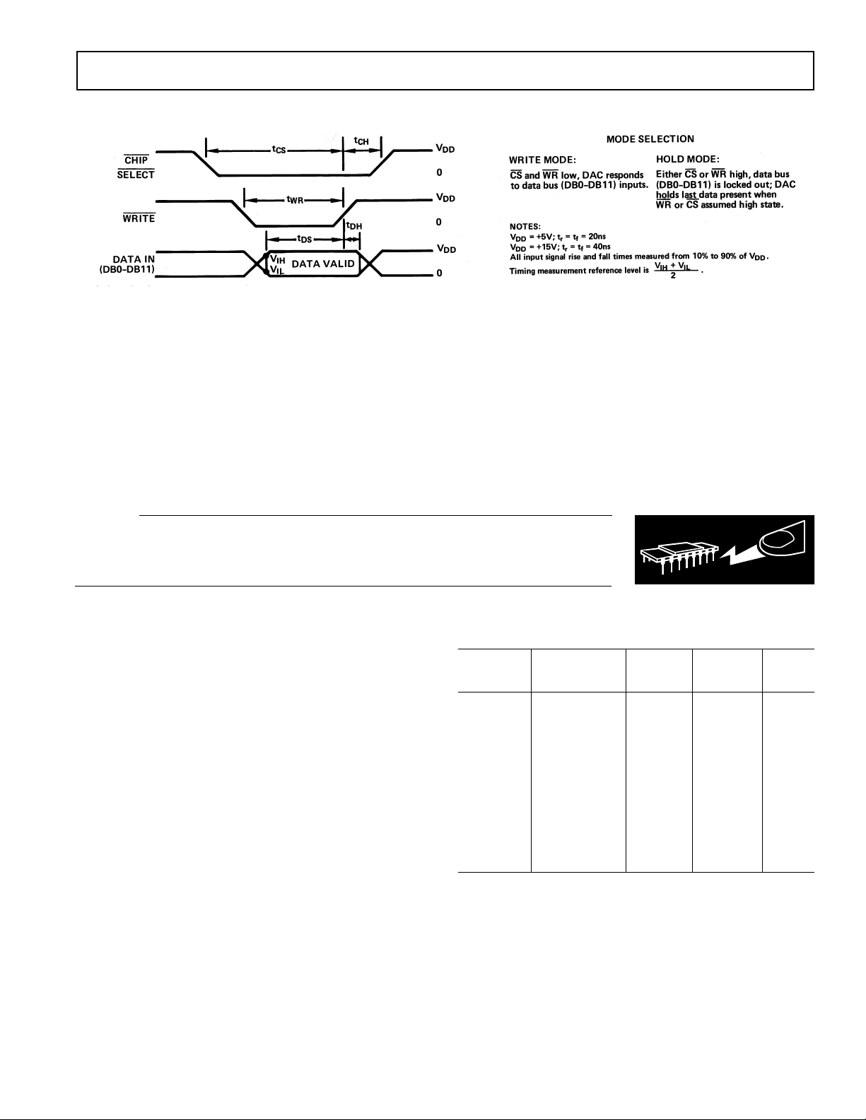
WRITE CYCLE TIMING DIAGRAM
WARNING!
ESD SENSITIVE DEVICE
AD7545A
ABSOLUTE MAXIMUM RATINGS*
(TA = + 25°C unless otherwise noted)
VDD to DGND . . . . . . . . . . . . . . . . . . . . . . . . . –0.3 V, +17 V
Digital Input Voltage to DGND . . . . . . . –0.3 V, V
, V
V
V
RFB
PIN1
to DGND . . . . . . . . . . . . . . . . . . . . . . . . . ± 25 V
REF
to DGND . . . . . . . . . . . . . . . . . . . . –0.3 V, VDD +0.3 V
AGND to DGND . . . . . . . . . . . . . . . . . . –0.3 V, V
+0.3 V
DD
+0.3 V
DD
Power Dissipation (Any Package) to 75°C . . . . . . . . . 450 mW
Derates above 75°C by . . . . . . . . . . . . . . . . . . . . . 6 mW/°C
Operating Temperature Range
Commercial (KN, LN, KP, LP) Grades . . . 0°C to +70°C
Industrial (BQ, CQ, BE, CE) Grades . . . . –25°C to +85°C
Extended (TQ, UQ, TE, UE) Grades . . . –55°C to +125°C
Storage Temperature . . . . . . . . . . . . . . . . . . –65°C to +150°C
Lead Temperature (Soldering, 10 secs) . . . . . . . . . . . +300°C
*Stresses above those listed under Absolute Maximum Ratings may cause perma-
nent damage to the device. This is a stress rating only; functional operation of the
device at these or any other conditions above those indicated in the operational
sections of this specification is not implied. Exposure to absolute maximum rating
conditions for extended periods may affect device reliability.
CAUTION
ESD (electrostatic discharge) sensitive device. The digital control inputs are diode protected;
however, permanent damage may occur on unconnected devices subject to high energy electrostatic fields. Unused devices must be stored in conductive foam or shunts. The protective foam
should be discharged to the destination socket before devices are removed.
ORDERING GUIDE
1
Model
AD7545AKN 0°C to +70°C ±1/2 ±4 N-20
AD7545ALN 0°C to +70°C ±1/2 ±2 N-20
AD7545AKR 0°C to +70°C ±1/2 ±4R-20
AD7545AKP 0°C to +70°C ±1/2 ±4 P-20A
AD7545ALP 0°C to +70°C ±1/2 ±2 P-20A
AD7545ABQ –25°C to +85°C ±1/2 ±4 Q-20
AD7545ACQ –25°C to +85°C ± 1/2 ±2 Q-20
AD7545ABE –25°C to +85°C ± 1/2 ±4 E-20A
AD7545ACE –25°C to +85°C ± 1/2 ±2 E-20A
AD7545ATQ –55°C to +125°C ± 1/2 ±4 Q-20
AD7545AUQ –55°C to +125°C ±1/2 ±2 Q-20
AD7545ATE –55°C to +125°C ±1/2 ±4 E-20A
AD7545AUE –55°C to +125°C ±1/2 ±2 E-20A
NOTES
1
To order MIL-STD-883, Class B process parts, add /883B to part number.
Contact local sales office for military data sheet.
2
E = Leadless Ceramic Chip Carrier (LCCC); N = Plastic DIP; P = Plastic
Leaded Chip Carrier (PLCC); Q = Cerdip; R = Small Outline IC.
Temperature Accuracy Error Package
Range T
Relative Gain
MIN–TMAXTMIN–TMAX
Options
2
–3–REV. C
 Loading...