10 MHz, Four-Quadrant
X1X
Y
FEATURES
High accuracy
0.1% typical error
High speed
10 MHz full power bandwidth
450 V/μs slew rate
200 ns settling to 0.1% at full power
Low distortion
−80 dBc from any input
Third-order IMD typically −75 dBc at 10 MHz
Low noise
94 dB SNR, 10 Hz to 20 kHz
70 dB SNR, 10 Hz to 10 MHz
Direct division mode
2 MHz BW at gain of 100
APPLICATIONS
High performance replacement for AD534
Multiply, divide, square, square root
Modulators, demodulators
Wideband gain control, rms-to-dc conversion
Voltage-controlled amplifiers, oscillators, and filters
Demodulator with 40 MHz input bandwidth
Multiplier/Divider
AD734
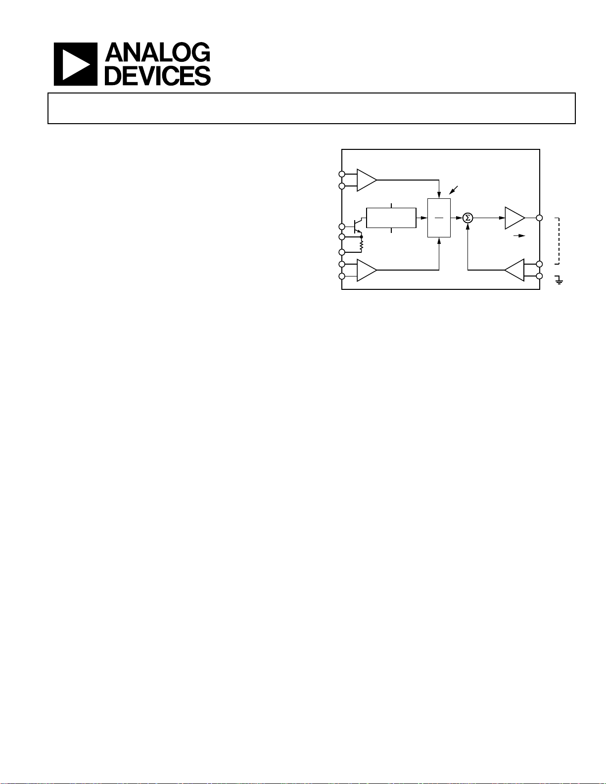
FUNCTIONAL BLOCK DIAGRAM
AD734
X = X1 – X
2
XZ
U
2
Figure 1.
HIGH ACCURAC Y
TRANSLINEAR CO RE
XY ÷ U – Z
+
–
Z = Z1 – Z
A
2
WIF
O
ZIF
W
∞
Z1
Z2
00827-003
XIF
2
DD
DENOMINATOR
YIF
CONTROL
R
U
ER
U0
U1
U2
1
Y2
U
Y = Y1 –Y
GENERAL DESCRIPTION
The AD734 is an accurate high speed, four-quadrant analog
multiplier that is pin compatible with the industry-standard
AD534 and provides the transfer function W = XY/U. The
AD734 provides a low impedance voltage output with a full
power (20 V p-p) bandwidth of 10 MHz. Total static error
(scaling, offsets, and nonlinearities combined) is 0.1% of full
scale. Distortion is typically less than −80 dBc and guaranteed.
The low capacitance X, Y, and Z inputs are fully differential.
In most applications, no external components are required to
define the function.
The internal scaling (denominator) voltage, U, is 10 V, derived
from a buried-Zener voltage reference. A new feature provides
the option of substituting an external denominator voltage,
allowing the use of the AD734 as a two-quadrant divider with a
1000:1 denominator range and a signal bandwidth that remains
10 MHz to a gain of 20 dB, 2 MHz at a gain of 40 dB, and 200 kHz
at a gain of 60 dB, for a gain-bandwidth product of 200 MHz.
The advanced performance of the AD734 is achieved by a
combination of new circuit techniques, the use of a high speed
complementary bipolar process, and a novel approach to laser
trimming based on ac signals rather than the customary dc
methods. The wide bandwidth (>40 MHz) of the AD734’s input
stages and the 200 MHz gain-bandwidth product of the multiplier
core allow the AD734 to be used as a low distortion demodulator
with input frequencies as high as 40 MHz as long as the desired
output frequency is less than 10 MHz.
The AD734AQ and AD734BQ are specified for the industrial
temperature range of −40°C to +85°C and come in a 14-lead
CERDIP and a 14-lead PDIP package. The AD734SQ/883B,
available processed to MIL-STD-883B for the military range of
−55°C to +125°C, is available in a 14-lead CERDIP.
Rev. E
Information furnished by Analog Devices is believed to be accurate and reliable. However, no
responsibility is assumed by Analog Devices for its use, nor for any infringements of patents or other
rights of third parties that may result from its use. Specifications subject to change without notice. No
license is granted by implication or otherwise under any patent or patent rights of Analog Devices.
Trademarks and registered trademarks are the property of their respective owners.
One Technology Way, P.O. Box 9106, Norwood, MA 02062-9106, U.S.A.
Tel: 781.329.4700 www.analog.com
Fax: 781.461.3113 ©2011 Analog Devices, Inc. All rights reserved.

AD734
TABLE OF CONTENTS
Features.............................................................................................. 1
Applications....................................................................................... 1
Functional Block Diagram .............................................................. 1
General Description ......................................................................... 1
Revision History ............................................................................... 2
Specifications..................................................................................... 3
Absolute Maximum Ratings............................................................ 5
Thermal Resistance ...................................................................... 5
ESD Caution.................................................................................. 5
Pin Configuration and Function Descriptions............................. 6
Typical Performance Characteristics ............................................. 7
REVISION HISTORY
2/11—Rev. D to Rev. E
Changes to Figure 4, Figure 5, and Figure 6.................................. 7
Changes to Figure 22 and Figure 23............................................. 12
Changes to Figure 27 and Figure 28............................................. 14
Changes to Figure 36...................................................................... 17
1/11—Rev. C to Rev. D
Updated Format..................................................................Universal
Changes to Figure 1 and General Description Section ............... 1
Deleted Product Highlights Section............................................... 1
Change to Endnote 3........................................................................ 4
Changes to Table 2 and Table 3....................................................... 5
Added Pin Configuration and Function Descriptions Section.. 6
Added Figure 3; Renumbered Sequentially .................................. 6
Added Table 4; Renumbered Sequentially .................................... 6
Changes to Functional Description Section ............................... 10
Changes to Figure 36...................................................................... 17
Updated Outline Dimensions....................................................... 19
Changes to Ordering Guide.......................................................... 19
Functional Description.................................................................. 10
Available Transfer Functions .................................................... 10
Direct Denominator Control.................................................... 11
Operation as a Multiplier.......................................................... 12
Operation as a Divider............................................................... 14
Division by Direct Denominator Control............................... 14
A Precision AGC Loop.............................................................. 15
Wideband RMS-to-DC Converter Using U Interface........... 16
Low Distortion Mixer................................................................ 17
Outline Dimensions....................................................................... 18
Ordering Guide .......................................................................... 19
Rev. E | Page 2 of 20

AD734
()(
)
SPECIFICATIONS
TA = +25°C, +VS = VP = +15 V, −VS = VN = −15 V, RL ≥ 2 kΩ, unless otherwise noted.
Generalized transfer function:
⎧
⎪
AW
=
⎨
O
⎪
⎩
YYXX
−−
2121
UU
−
21
()
⎫
⎪
ZZ
−−
⎬
21
⎪
⎭
Table 1.
A B S
Parameter Conditions Min Typ Max Min Typ Max Min Typ Max Unit
MULTIPLIER PERFORMANCE
Transfer Function W =
Total Static Error1 −10 V ≤ X, Y ≤ 10 V 0.1 0.4 0.1 0.25 0.1 0.4 %
Over T
vs. Temperature T
vs. Either Supply ±VS = 14 V to 16 V 0.01 0.05 0.01 0.05 0.01 0.05 %/V
Peak Nonlinearity −10 V ≤ X ≤ +10 V,
−10 V ≤ Y ≤ +10 V,
THD2 X = 7 V rms, Y =
T
Y = 7 V rms, X =
T
Feedthrough X = 7 V rms, Y =
Y = 7 V rms, X =
Noise (RTO) X = Y = 0 V
Spectral Density 100 Hz to 1 MHz 1.0 1.0 1.0 μV/√Hz
Total Output Noise 10 Hz to 20 kHz −94 −88 −94 −88 −94 −88 dBc
T
DIVIDER PERFORMANCE
(Y = 10 V)
Transfer Function W =
Gain Error Y = 10 V, U = 100 mV
X Input Clipping Level Y ≤ 10 V 1.25 × U 1.25 × U 1.25 × U V
U Input Scaling Error3 0.3 0.15 0.3 %
T
Output to 1% U = 1 V to 10 V step,
INPUT INTERFACES
(X, Y, AND Z)
3 dB Bandwidth 40 40 40 MHz
Operating Range Differential or
X Input Offset Voltage 15 5 15 mV
T
Y Input Offset Voltage 10 5 10 mV
T
Z Input Offset Voltage 20 10 20 mV
T
Z Input PSRR (Either
T
MIN
Supply)
to T
1 0.6 1.25 %
MAX
to T
MIN
Y = +10 V
X = +10 V
+10 V, f ≤ 5 kHz
MIN
+10 V, f ≤ 5 kHz
MIN
nulled, f ≤ 5 kHz
nulled, f ≤ 5 kHz
MIN
to 10 V
MIN
X = 1 V
common mode
MIN
MIN
MIN
f ≤ 1 kHz 54 70 66 70 54 70 dB
MIN
0.004 0.003 0.004 %/°C
MAX
0.05 0.05 0.05 %
0.025 0.025 0.025 %
−58 −66 −58 dBc
to T
−55 −63 −55 dBc
MAX
−60 −80 −60 dBc
to T
−57 −74 −57 dBc
MAX
−85 −60 −85 −70 –85 –60 dBc
−85 −66 −85 −76 −85 −66 dBc
to T
−85 −85 −85 dBc
MAX
1 1 1 %
to T
0.8 0.65 1 %
MAX
100 100 100 ns
±12.5 ±12.5 ±12.5 V
to T
25 15 25 mV
MAX
to T
12 6 12 mV
MAX
to T
50 50 90 mV
MAX
to T
50 56 50 dB
MAX
XY/10
XY/U
W =
XY/10
W =
XY/U
W =
XY/10
W =
XY/U
Rev. E | Page 3 of 20

AD734
A B S
Parameter Conditions Min Typ Max Min Typ Max Min Typ Max Unit
CMRR f = 5 kHz 70 85 70 85 70 85 dB
Input Bias Current
(X, Y, Z Inputs)
T
Input Resistance Differential 50 50 50 kΩ
Input Capacitance Differential 2 2 2 pF
DENOMINATOR INTERFACES
(U0, U1, AND U2)
Operating Range VN to
Denominator Range 1000:1 1000:1 1000:1
Interface Resistor U1 to U2 28 28 28 kΩ
OUTPUT AMPLIFIER (W)
Output Voltage Swing T
Open-Loop Voltage Gain X = Y = 0, input to Z 72 72 72 dB
Dynamic Response From X or Y input,
3 dB Bandwidth W ≤ 7 V rms 8 10 8 10 8 10 MHz
Slew Rate 450 450 450 V/μs
Settling Time +20 V or −20 V
To 1% 125 125 125 ns
To 0.1% 200 200 200 ns
Short-Circuit Current T
POWER SUPPLIES, ±VS
Operating Supply Range ±8 ±16.5 ±8 ±16.5 ±8 ±16.5 V
Quiescent Current T
1
Figures given are percent of full scale (for example, 0.01% = 1 mV).
2
dBc refers to decibels relative to the full-scale input (carrier) level of 7 V rms.
3
See for test circuit. Figure 28
50 300 50 150 50 300 nA
to T
MIN
400 300 500 nA
MAX
MIN
VP − 3
to T
±12 ±12 ±12 V
MAX
VP − 3
VN to
VN to
V
VP − 3
C
≤ 20 pF
LOAD
output step
to T
MIN
MIN
20 50 80 20 50 80 20 50 80 mA
MAX
to T
6 9 12 6 9 12 6 9 12 mA
MAX
Rev. E | Page 4 of 20
AD734
ABSOLUTE MAXIMUM RATINGS
Table 2.
Parameter Rating
Supply Voltage ±18 V
Internal Power Dissipation
for TJ max = 175°C 500 mW
X, Y, and Z Input Voltages VN to VP
Output Short-Circuit Duration Indefinite
Storage Temperature Range
Q-14 −65°C to +150°C
N-14 −65°C to +150°C
Operating Temperature Range
AD734A, AD734B (Industrial) −40°C to +85°C
AD734S (Military) −55°C to +125°C
Lead Temperature Range (Soldering, 60 sec) +300°C
Transistor Count 81
ESD Rating 500 V
Stresses above those listed under Absolute Maximum Ratings
may cause permanent damage to the device. This is a stress
rating only; functional operation of the device at these or any
other conditions above those indicated in the operational
section of this specification is not implied. Exposure to absolute
maximum rating conditions for extended periods may affect
device reliability.
THERMAL RESISTANCE
θJA is specified for the worst-case conditions, that is, a device
soldered in a circuit board for surface-mount packages.
Table 3. Thermal Resistance
Package Type θJA Unit
14-Lead PDIP (N-14) 150 °C/W
14-Lead CERDIP (Q-14) 110 °C/W
ESD CAUTION
W
12
DD
13
VP
X1
14
1
2
X2
0.093 (2.3622)
Z1
11
Z2
10
ER
9
8
7
6
VN
0.122
(3.0988)
Y2
Y1
3
U0
U1
54
U2
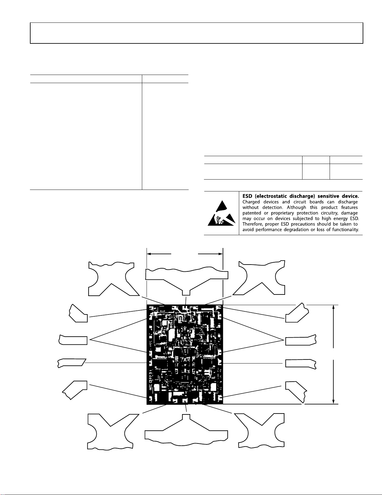
Figure 2. Chip Dimensions and Bonding Diagram, Dimensions shown in inches and (mm), (Contact factory for latest dimensions)
Rev. E | Page 5 of 20
00827-002
AD734
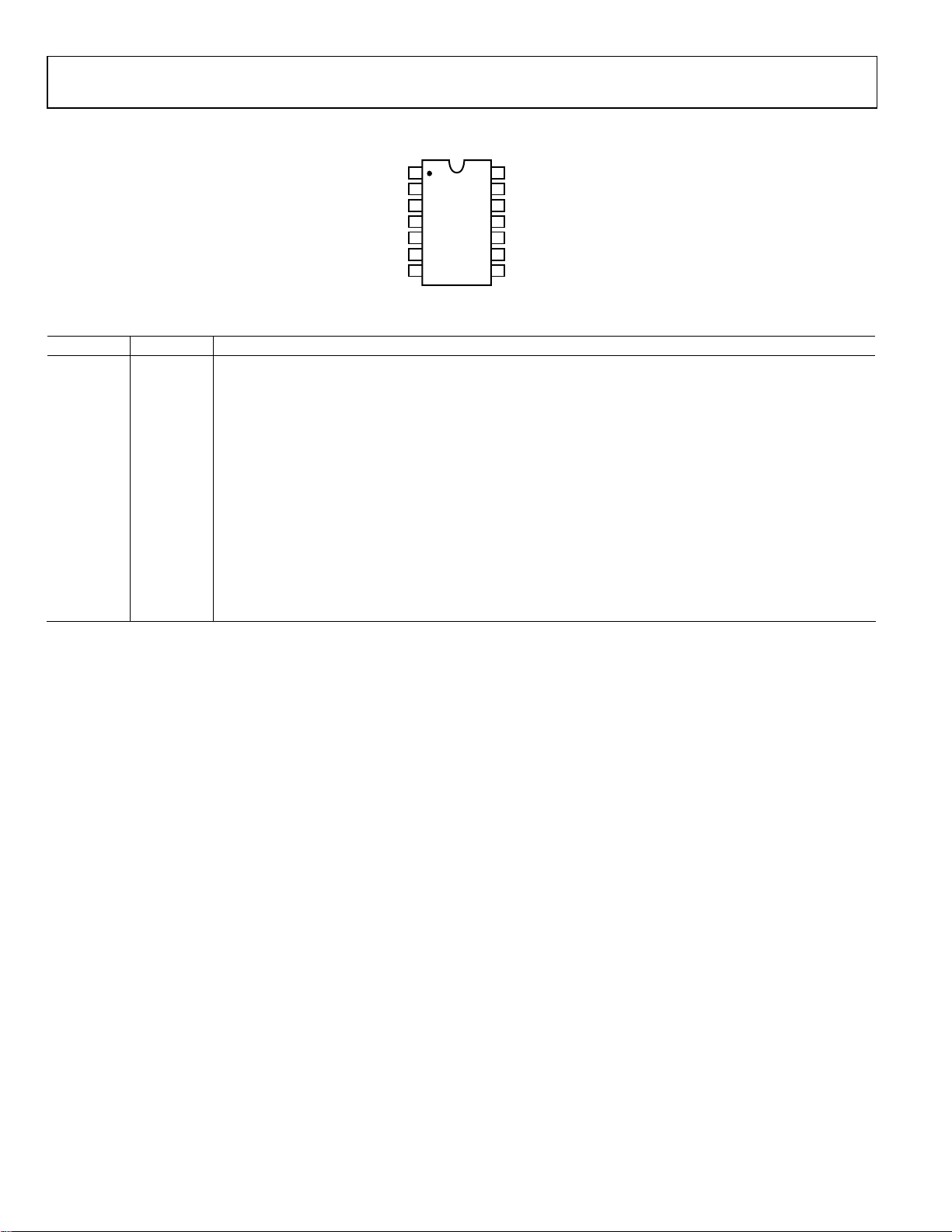
PIN CONFIGURATION AND FUNCTION DESCRIPTIONS
X1
X2
U0
U1
U2
Y1
Y2
1
2
AD734
3
TOP VIEW
(Not to S cale)
4
5
6
7
14
VP
DD
13
W
12
Z1
11
10
Z2
ER
9
VN
8
00827-001
Figure 3. 14-Lead PDIP and 14-Lead CERDIP
Table 4. Pin Function Descriptions
Pin No. Mnemonic Description
1 X1 X Differential Multiplicand Input.
2 X2 X Differential Multiplicand Input.
3 U0 Denominator Current Source Enable Interface.
4 U1 Denominator Interface—see the Functional Description section.
5 U2 Denominator Interface—see the Functional Description section.
6 Y1 Y Differential Multiplicand Input.
7 Y2 Y Differential Multiplicand Input.
8 VN Negative Supply.
9 ER Reference Voltage.
10 Z2 Z Differential Summing Input.
11 Z1 Z Differential Summing Input.
12 W Output.
13 DD Denominator Disable.
14 VP Positive Supply.
Rev. E | Page 6 of 20
 Loading...