Analog Devices AD7339 Datasheet

5 V Integrated High Speed ADC/Quad
DA7
DA0
VREFA
DVDD1
DGND1
AGND1
SDAC0F
DACA
AD7339
T/H
AVDD
DAC A
REGISTER
ADC
PARALLEL
DAC A
DB7
DB0
DACB
DACCLK
D0
D7
DAC 0
REGISTER
SERIAL
DAC 0
DAC 1
REGISTER
SERIAL
DAC 1
SERIAL
CONTROL
LOGIC
DAC B
REGISTER
PARALLEL
DAC B
2.5V
REFERENCE
SDAC0S
SDAC1F
SDAC1S
VREF
VREFB
ADCPDB
AIN
ADCCLK
DACPDB
SDATA
SCLK
LATCH
SDACPDB
DVDD2 DVDD3
DGND2
DGND3 AGND2 AGND3
a
FEATURES
8-Bit A/D Converter
Two 8-Bit D/A Converters
Two 8-Bit Serial D/A Converters
Single +5 V Supply Operation
On-Chip Reference
Power-Down Mode
52-Lead PQFP Package
GENERAL DESCRIPTION
The AD7339 is a composite IC that contains both DAC and
ADC functions. The device includes an 8-bit parallel A-to-D
converter. Two 8-bit parallel DACs are also included as are two
serial control DACs. These serial DACs are 8-bit DACs.
The AD7339, which operates with a single 5 V power supply,
has a bandgap reference on board with a nominal value of 2.5 V.
To reduce the power consumption of the part, each section,
except the reference, can be individually powered down when
not in use.
The AD7339 is available in a 52-lead PQFP package.
DAC System
AD7339
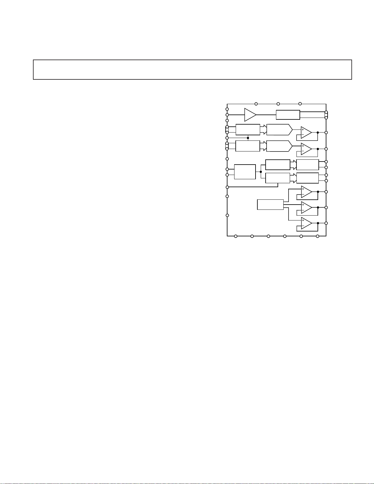
FUNCTIONAL BLOCK DIAGRAM
REV. 0
Information furnished by Analog Devices is believed to be accurate and
reliable. However, no responsibility is assumed by Analog Devices for its
use, nor for any infringements of patents or other rights of third parties
which may result from its use. No license is granted by implication or
otherwise under any patent or patent rights of Analog Devices.
One Technology Way, P.O. Box 9106, Norwood, MA 02062-9106, U.S.A.
Tel: 781/329-4700 World Wide Web Site: http://www.analog.com
Fax: 781/326-8703 © Analog Devices, Inc., 1997

(AVDD = DVDD = +5 V 6 10%, AGND = DGND = 0 V, TA = T
± V
1
wise noted)
coupling with a 1 nF capacitor is needed if the bias
voltage does not equal 1.4 V. The input should be
driven with a maximum source impedance of 50 Ω.
11
SWING
DACB and VREFB
AD7339–SPECIFICATIONS
Parameter B Version Units Test Conditions/Comments
ADC ADCCLK = 2.048 MHz
Resolution 8 Bits
Differential Nonlinearity ±1 LSB max 8 Bits Monotonic
Integral Nonlinearity ±1 LSB max
Zero Input Offset Error ±3 LSB
Signal Range ±1 V max The input must be biased about 1.4 V. Therefore, ac
Full Power Input Bandwidth 1.024 MHz
Conversion Rate 2.048 MSPS
Signal to (Noise + Distortion) 42.7 dB min
Effective No. of Bits (ENOB) 6.8 Bits min
Intermodulation Distortion 48 dB min See Terminology
Error Rate 4.7 × 10
Input Capacitance 5 pF max
Coding Offset Binary 00H to FFH with 80H = 0 V
PARALLEL DACS DACCLK = 2.304 MHz
Resolution 8 Bits
Differential Nonlinearity ±1 LSB max 8 Bits Monotonic
Integral Nonlinearity ±1 LSB max
Output Signal Range V
V
SWING
V
BIAS
Update Rate 2.304 MHz max
Bipolar Zero Offset Error ±40 mV max Factory Trim. Does Not Include Gain Error
Gain Error ±5 % typ
Output Harmonic Content in 50 dB min For a Full-Scale Digital Sine Wave in Band 0 kHz to 76.8 kHz
Band 0 MHz to 1.152 MHz 46 dB min For a Full-Scale Digital Sine Wave in Band 0 kHz to 128 kHz
Gain Matching Between DACs 0.2 dB For Amplitudes Which Equal Full Scale –10 dB
Crosstalk 1.8 kΩ Load Between DACA and VREFA, and Between
To B Channel from A Channel 55 dB min A Channel has a full-scale output of frequency 128 kHz.
To A Channel from B Channel 55 dB min B Channel has a full-scale output of frequency 128 kHz.
To VREFB from A Channel 55 dB min A Channel has a full-scale output of frequency 128 kHz.
To VREFA from B Channel 55 dB min B Channel has a full-scale output of frequency 128 kHz.
Load Resistance 1.8 kΩ min Connected Between DACA/B and VREFA/B
Load Capacitance 50 pF max
Full-Scale Settling Time 4 µs typ
Coding Offset Binary 00H to FFH with 80H = Bias Voltage
BIAS
14/25 × VREFA/B V nom VREFA/B means VREFA for DACA and VREFB for DACB.
VREFA/B V nom
MIN
to T
MAX
, unless other-
SERIAL DACS SCLK is a gated 256 kHz clock.
Resolution 8 Bits
Differential Nonlinearity ±1 LSB 8 Bits Monotonic
Integral Nonlinearity ±1.5 LSB With Respect to Full Scale
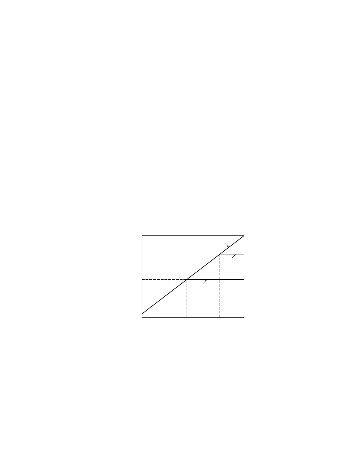
Output Range See Figure 1
00H 0.2 V max
FFH AVDD – 0.247 V min When AVDD > 5.247 V, the analog output will equal 2 VREF.
Update Rate SCLK/10 kHz max
Load Resistance 20 kΩ max
Load Capacitance 100 pF max
I
SINK
I
SOURCE
Full-Scale Settling Time 2.5 µs typ
Coding Straight Binary
1 mA typ
100 µA typ
–2–
REV. 0

AD7339
Parameter B Version Units Test Conditions/Comments
REFERENCE
VREF Voltage 2.5 ± 2% V min/max
VREFA/VREFB Voltage 2.5 ± 5% V min/max
Load Capacitance 0.1 µF max Each reference output must have a load capacitance
of 100 pF minimum for compensation purposes.
I
SINK
I
SOURCE
LOGIC INPUTS
V
, Input High Voltage DVDD – 0.8 V min
INH
V
, Input Low Voltage 0.8 V max
INL
I
, Input Leakage Current 10 µA max
INH
CIN, Input Capacitance 15 pF max
LOGIC OUTPUTS
V
, Output High Voltage DVDD – 0.4 V min |I
OH
V
, Output Low Voltage 0.4 V max |I
OL
C
, Output Capacitance 15 pF max
OUT
POWER SUPPLIES
AVDD, DVDD 4.5/5.5 V min/max
I
DD
Power-Down Current 4.5 mA max +25°C. No Load on VREF
NOTES
1
Operating temperature range is as follows: B Version; –40° C to +85°C.
Specifications subject to change without notice.
1 mA max
1 mA max
| ≤ 1 mA
OUT
| ≤ 2 mA
OUT
45 mA max Active Mode
5 mA max –40°C to +85°C. No Load on VREF
2VREF
4.753
4.253
POWER
OUTPUT VOLTAGE – Volts
0.2
0 255
ANALOG OUTPUT VOLTAGE
SUPPLY
217 243
+4.5V
+5.5V
POWER
SUPPLY
+5V
POWER
SUPPLY
Figure 1. Analog Output Voltage from Serial DACs vs. Power Supply
REV. 0
–3–

AD7339
TIMING CHARACTERISTICS
(AVDD = +5 V 6 10%; AGND = DGND = 0 V; TA = T
Limit at
Parameter TA = –408C to +858C Units Description
ADC See Figure 3.
t
1
t
2
t
3
t
4
t
5
480 ns min ADCCLK Period
210 ns min ADCCLK Width Low
210 ns min ADCCLK Width High
100 ns min Data Valid After Falling Edge of ADCCLK
200 ns min Data Valid Before Subsequent Falling Edge of ADCCLK
PARALLEL DACS See Figure 4.
t
6
t
7
t
8
t
9
t
10
t
11
t
12
430 ns min DACCLK Period
200 ns min DACCLK Width Low
200 ns min DACCLK Width High
130 ns min Data Setup Before DACCLK Rising Edge Time
50 ns min Data Hold After DACCLK Rising Edge Time
150 ns max Propagation Delay
250 ns max Settling Time (from 10% to 90%)
SERIAL DACS See Figure 5.
t
13
t
14
t
15
t
16
t
17
t
18
t
19
3.9 µs min SCLK Period
1.94 µs min SCLK Width Low
1.94 µs min SCLK Width High
950 ns min Data Setup Before SCLK Rising Edge
950 ns min Latch Enable Setup Time After SCLK Falling Edge
480 ns min LATCH Pulsewidth
100 µs max Conversion Delay
MlN
to T
, unless otherwise noted)
MAX
I
2mA
OL
TO
OUTPUT
PIN
15pF
C
L
I
1mA
OH
+2.1V
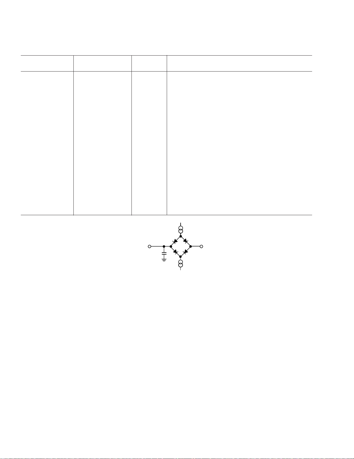
Figure 2. Load Circuit for Timing Specifications
–4–
REV. 0
 Loading...