250 ksps, 8-Channel, Software Selectable
© 2005
True bipolar Input, 12-Bit Plus Sign ADC
Preliminary Technical Data
FEATURES
12-Bit Plus Sign SAR ADC
Accepts True Bipolar Analog Inputs
Software Selectable input Ranges
±10V, ±5V, ±2.5V, 0 to 10 V
Eight Analog Input Channels with Channel Sequencer
Single Ended, True Differential and Pseudo Differential
Analog Input Capability.
High Impedance Analog Inputs
Low Power: 12 mW
Full Power Bandwidth of > TBD MHz
High Speed Serial Interface SPI/QSPI/DSP/MICROWIRE
Compatible
Mux Out and ADC in pins allows separate access to Mux and
ADC
TM
iCMOS
24 Lead TSSOP package
PRODUCT OVERVIEW
The AD7329 is an 8-Channel, 12-Bit Plus Sign Successive
Approximation ADC. The ADC has a high-speed serial
interface that can operate at throughput rates up to TBD ksps.
The AD7329 can accept True Bipolar Analog input signals. The
Ad7329 has four software selectable ranges, ±10V, ±5V, ±2.5V
and 0 to 10V. Each analog input channel can be independently
programmed to one of the input ranges by setting the
appropriate bits in the Range Registers.
The Analog Input Channels can be configured as single ended,
fully differential or pseudo differential. Dedicated Control
Register bits are used to configure the Analog inputs.
The ADC contains a 2.5V Internal reference. The AD7329 also
allows for external Reference operation. If a 3V external
reference is applied to the REFIN/OUT pin, the ADC can
handle a True Bipolar ± 12 V Analog input range. V
supplies of ± 12V are required for this ± 12 V input range.
Process Technology
and VSS
DD
AD7329*
FUNCTIONAL BLOCK DIAGRAM
MUX
OUT (+)
Vin0
Vin1
Vin2
Vin3
I/P
MUX
Vin4
Vin5
Vin6
Vin7
CHANNEL
SEQUENCER
AD7329
The AD7329 has multiplexer output pins and ADC input pins.
These allow the user to insert buffers, differential amplifiers or
antialiasing filters, if required, between the Multiplexer and the
ADC. This means that for eight analog inputs only a single
driver is required for the AD7329.
The AD7329 has a number of power down mode to reduce
power consumption at lower throughput rates.
PRODUCT HIGHLIGHTS
1. The AD7329 can accept True Bipolar Analog Input signals,
±10V, ±5V, ±2.5V and 0 to 10V unipolar signals.
2. The Eight Analog Inputs can be configured as 8 Single-Ended
inputs, 4 True Differential, 4 Pseudo Differential or 7 Pseudo
Differential Inputs.
3. SPI/QSPI/DSP/MICROWIRE compatible Interface.
4. Low Power, TBD mW at maximum throughput rate.
5. Channel Sequencer..
ADC
MUX
OUT (-)
IN (-)
ADC
IN (+)
V
REFIN/OUT
DD
T/H
V
SS
Figure 1. AD7329 Block Diagram
V
CC
2.5V
VREF
13-BIT SUCCESSIVE
APPROXIMATION
ADC
CONTROL
LOGIC &
REGISTERS
V
DRIVE
AGND
DOUT
SCLK
+5
DIN
* Protected by U.S. Patent No. 6,731,232
TM
iCMOS
Process Technology
For analog systems designers within industrial/instrumentation equipment OEMs who need high performance ICs at higher-voltage levels, iCMOS is a technology platform
that enables the development of analog ICs capable of 30V and operating at +/- 15V supplies while allowing dramatic reductions in power consumption and package size, and
increased AC and DC performance.
Rev. PrB
Information furnished by Analog Devices is believed to be accurate and reliable.
However, no responsibility is assumed by Analog Devices for its use, nor for any
infringements of patents or other rights of third parties that may result from its use.
Specifications subject to change without notice. No license is granted by implication
or otherwise under any patent or patent rights of Analog Devices. Trademarks and
registered trademarks are the property of their respective companies.
One Technology Way, P.O. Box 9106, Norwood, MA 02062-9106, U.S.A.
Tel: 781.329.4700
Fax: 781.326.8703 © 2004 Analog Devices, Inc. All rights reserved.
www.analog.com

Preliminary technical Data
TABLE OF CONTENTS
AD7329*
AD7329—SPECIFICATIONS ............................ 3
ABSOLUTE MAXIMUM RATINGS ................. 7
PIN FUNCTIONAL DESCRIPTIONS........................... 8
TERMINOLOGY.............................................. 10
THEORY OF OPERATION....................................... 11
AD7329 REGISTERS........................................ 15
REVISION HISTORY
Revision PrB: Preliminary Version
SEQUENCER OPERATION............................. 19
MODES OF OPERATION ................................ 23
SERIAL INTERFACE....................................... 24
OUTLINE DIMENSIONS................................. 25
Rev. PrB | Page 2 of 25
Preliminary Technical Data AD7329
AD7329—SPECIFICATIONS
Table 1. Unless otherwise noted, VDD = + 12V to +16.5V, VSS = -12V to –16.5V, VCC = 2.7V to 5.25V, V
2.5V Internal/External, f
Parameter Specification Units Test Conditions/Comments
DYNAMIC PERFORMANCE
Signal to Noise Ratio (SNR)
72 dB min Single-Ended/Pesudo Differential Mode
Signal to Noise + Distortion (SINAD)2 75 dB min Differential Mode
71.5 dB min Single-Ended/Pseudo Differential Mode
Total Harmonic Distortion (THD)
Peak Harmonic or Spurious Noise
2
(SFDR)
Intermodulation Distortion (IMD)
Second Order Terms -88 dB typ
Third Order Terms
Aperature Delay
Aperature Jitter
Common Mode Rejection (CMRR) TBD dB typ
Channel-to-Channel Isolation
Full Power Bandwidth
DC ACCURACY
Resolution 12 + Sign Bits
Integral Nonlinearity
Differential Nonlinearity
Offset Error2 ±8 LSB max Unipolar Range with Straight Binary output coding
Offset Error Match ±0.5 LSB max
Gain Error2 ±6 LSB max
Gain Error Match ±0.6 LSB max
Positive Full-Scale Error
Positive Full Scale Error Match ±0.6 LSB max
Bipolar Zero Error2 ±8 LSB max
Bipolar Zero Error Match ±0.5 LSB max
Negative Full Scale Error2 ±4 LSB max
Negative Full Scale Error Match ±0.5 LSB max
ANALOG INPUT
Input Voltage Ranges
(Programmed via Range Register)
DC Leakage Current ±10 nA max
Input Capacitance 12 pF typ When in Track, ±10V Range
15 pF typ When in Track, ±5V, 0 to 10V Range
20 pF typ When in Track, ±2.5V Range
3 pF typ When in Hold
REFERENCE INPUT/OUTPUT
Input Voltage Range +2.5 to +3V
Input DC Leakage Current ±1 µA max
Input Capactiance 20 pF typ
Reference Output Voltage 2.49/2.51 Vmin/max
= 5 MHz, fS = 250 ksps TA = T
SCLK
2
2
2
2
2
2
1
= 2.7V to 5.25V, V
DRIVE
to T
MAX
F
76 dB min Differential Mode
-80 dB max
-80
dB max
F
-88 dB typ
10 ns max
50 ps typ
-80 dB typ F
TBD
TBD
MHz typ
MHz typ
±1.5 LSB max
± 0.95 LSB max Guaranteed No Missing Codes to 13-Bits
±3 LSB max Bipolar Range with Twos Complement Output Coding
±10V
Volts VDD = +10V min , VSS = -10V min, VCC = 2.7V to 5.25V
±5V
±2.5V
0 to 10V
V min to
max
MIN
= 50 kHz Sine Wave
IN
= 40.1 kHz, Fb = 41.5 kHz
a
= TBD kHz
IN
@ 3 dB
@ 0.1 dB
V
= +5V min, VSS = -5V min, VCC = 2.7V to 5.25V
DD
V
= +5V min, VSS = - 5V min, VCC = 2.7V to 5.25V
DD
= +10V min, VSS = AGND min, VCC = 2.7V to 5.25V
V
DD
See Table 5
REF
=
Rev. PrB | Page 3 of 25

AD7329 Preliminary Technical Data
Parameter Specification Units Test Conditions/Comments
Reference Temperature Coefficient 25 ppm/°C max
10 ppm/°C typ
Reference Output Impedance 25
LOGIC INPUTS
Input High Voltage, V
Input Low Voltage, V
2.4 V min
INH
0.8 V max V
INL
Ω typ
0.4 V max V
Input Current, IIN ± 1 µA max VIN = 0V or VCC
Input Capacitance, C
3
IN
10 pF max
LOGIC OUTPUTS
Output High Voltage, VOH V
- 0.2V V min I
DRIVE
Output Low Voltage, VOL 0.4 V max I
Floating State Leakage Current ±1 µA max
Floating State Output Capacitance
Output Coding
3
10 pF max
Straight
Coding bit set to 1 in Control Register
Natural
Binary
Two’s
Coding bit set to 0 in Control Register
Complement
CONVERSION RATE
Conversion Time 3.2 µs max 16 SCLK Cycles with SCLK = 5 MHz
Track-and-Hold Acquisition Time TBD ns min Sine Wave Input
TBD ns min Full Scale Step input
Throughput Rate 250 kSPS max See Serial Interface section
POWER REQUIREMENTS
4
V
12V/+16.5V V min/max See Table 5
DD
4
V
-12V/16.5V V min/max See Table 5
SS
Digital Inputs = 0V or VCC
VCC 2.7V / 5.25V V min/max See Table 5
V
2.7V/5.25V V min/max
DRIVE
Normal Mode
IDD 300 µA max VDD = +16.5V
ISS 370 µA max VSS = -16.5V
ICC 2 mA max VCC = 5.25V
Auto-Standby Mode F
IDD TBD µA max
ISS TBD µA max
ICC 1.6 mA typ
Auto-Standby Mode F
IDD TBD µA max
ISS TBD µA max
ICC 1 mA typ
Full Shutdown Mode
IDD 0.9 µA max
ISS 0.9 µA max
ICC 0.9 µA max SCLK On or Off
POWER DISSIPATION
Normal Mode 26 mW max V
12 mW typ V
Full Shutdown Mode 35 µW max V
= 4.75 to 5.25 V
CC
= 2.7 to 3.6 V
CC
= 200 µA
SOURCE
= 200 µA
SINK
= TBD
SAMPLE
= TBD
SAMPLE
= +16.5V, VSS = -16.5V, V
DD
= +5V, VSS = -5V, V
DD
= +16.5V, VSS = -16.5V, V
DD
CC
= 5V,
= 5.25V,
CC
= 5.25V,
CC
Rev. PrB | Page 4 of 25

Preliminary Technical Data AD7329
NOTES
1
Temperature ranges as follows: -40°C to +85°C
2
See Terminology
3
Guaranteed by initial Characterization
4
Functional from VDD = +4.75V and VSS = -4.75
Specifications subject to change without notice.
Rev. PrB | Page 5 of 25
Preliminary technical Data
TIMING SPECIFICATIONS
Table 2. Unless otherwise noted,
2.5V Internal/External, T
Parameter Limit at T
f
SCLK
20 kHz min
5 MHz max
t
CONVERT
t
50 ns min
QUIET
t
1
t
2
t
3
t
4
16×t
10 ns min
10 ns min
20 ns max
TBD ns max Data Access Time after SCLK Falling Edge.
t5 0.4t
t6 0.4t
t
7
t
8
10 ns min SCLK to Data Valid Hold Time
25 ns max SCLK Falling Edge to D
10 ns min SCLK Falling Edge to D
t
9
t
10
TBD ns min DIN set-up time prior to SCLK falling edge
5 ns min DIN hold time after SCLK falling edge
1 µs max Power up from Auto Standby
TBD µs max Power up from Full Shutdown/Auto Shutdown Mode
MIN
ns max T
SCLK
SCLK
ns min SCLK High Pulsewidth
SCLK
VDD = +12V to + 16.5V, VSS = -12 to –16.5V, V
= T
to T
MIN
Unit Description
SCLK
= 1/f
SCLK
Minimum Time between End of Serial Read and Next Falling Edge of
Minimum CS pulse width
CS
to SCLK Setup Time
Delay from CS until D
ns min SCLK Low Pulsewidth
, T
A
MAX
MAX
Three-State Disabled
OUT
High Impedance
OUT
High Impedance
OUT
=2.7V to 5.25, V
CC
=2.7V to 5.25, V
DRIVE
AD7329*
=
REF
CS
+5
SCLK
DOUT
DIN
t
2
3-STATE
1
t
3 IDENTIFICATION BITS
ADD2
WRITE
3
ADD1
Reg Sel1
2
ADD0
t
9
t
convert
t
6
t
DB11
5
t
4
DB10
7
t
10
34
SIGN
MSBReg Sel2
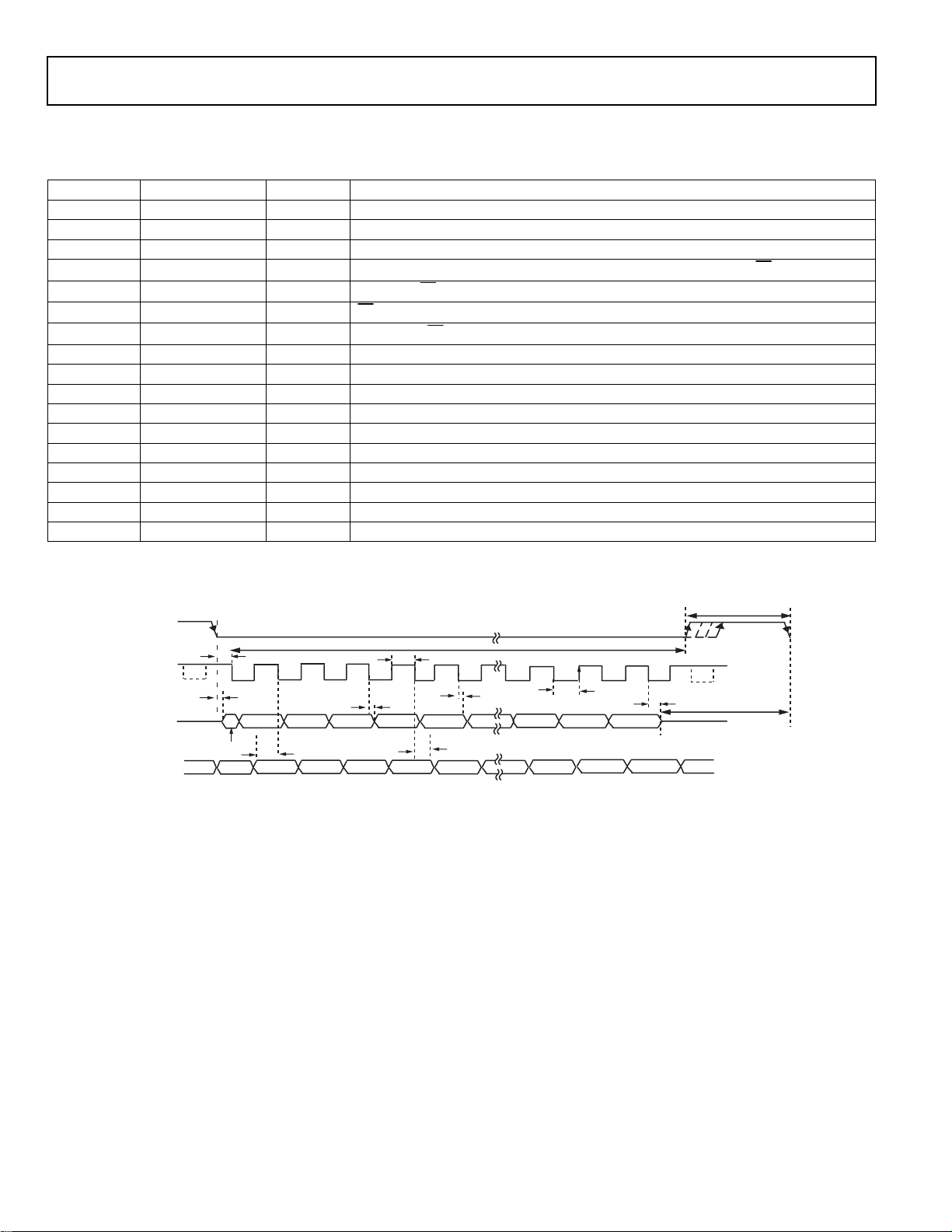
Figure 2. Serial Interface timing Diagram
t
1
13
14
t
DB2
15
16
5
DB1
LSB
DB0
t
8
DONTC
3-STATE
t
QUIET
Rev. PrB | Page 6 of 25

Preliminary technical Data
ABSOLUTE MAXIMUM RATINGS
Table 3. TA = 25°C, unless otherwise noted
VDD to AGND, DGND -0.3 V to +16.5 V
VSS to AGND, DGND +0.3 V to –16.5 V
VCC to AGND, DGND -0.3V to +7V
V
to DGND -0.3 V to + 7V
DRIVE
AGND to DGND -0.3 V to +0.3 V
Analog Input Voltage to AGND
ADC_IN(-), ADC_IN(+) to AGND
MUX_OUT(-), MUX_OUT(+) to AGND
Digital Input Voltage to DGND -0.3 V to +7 V
Digital Output Voltage to GND -0.3 V to V
REFIN to AGND -0.3 V to VCC +0.3V
Input Current to Any Pin Except Supplies
Operating Temperature Range -40°C to +85°C
Storage Temperature Range -65°C to +150°C
Junction Temperature +150°C
TSSOP Package
θJA Thermal Impedance 143 °C/W
θJC Thermal Impedance 45 °C/W
Pb/SN Temperature, Soldering
Reflow (10 s to 30 s) 240(+0/-5)°C
Pb-free Temperature, Soldering
Reflow 260(+0)°C
ESD TBD
-0.5V to +VDD +
V
SS
-0.5V to +VDD +
V
SS
-0.5V to +VDD +
V
SS
2
DRIVE
±10mA
0.5V
0.5V
0.5V
+0.3V
AD7329*
Rev. PrB | Page 7 of 25
Preliminary technical Data
Pin Functional Descriptions
DGND
AGND
REFIN/REF
ADCIN(+)
MUX
OUT
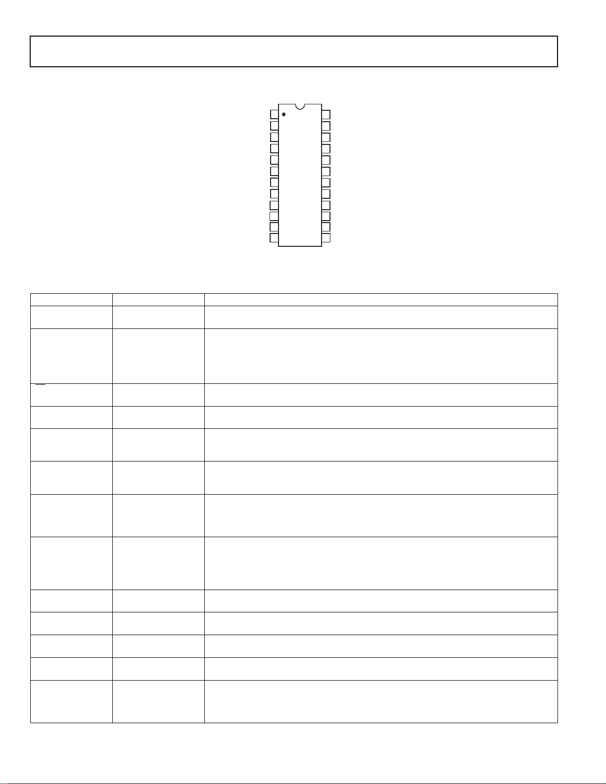
Figure 3. AD7329 Pin Configuration TSSOP
Table 4. AD7329 Pin Function Descriptions
Pin Mnemonic Pin Number Description
SCLK 24
D
22
OUT
CS
1
DIN 2
V
21
DRIVE
DGND 3, 23
AGND 4
REF
REF
IN/
5
OUT
VCC 20
VDD 19
VSS 6
ADCIN(+) 7
MUX
(+) 8
OUT
Serial Clock. Logic Input. A serial clock input provides the SCLK used for accessing the data
from the AD7329. This clock is also used as the clock source for the conversion process.
Serial Data Output. The conversion output data is supplied to this pin as a serial data stream.
The bits are clocked out on the falling edge of the SCLK input and 16 SCLKs are required to
access the data. The data stream consists of three channel identification bits, followed by the
sign bit followed by the 12 bits of conversion data. The data is provided MSB first.
See the Serial Interface section.
Chip Select. Active low logic input. This input provides the dual function of initiating
conversions on the AD7329 and frames the serial data transfer.
Data In. Data to be written to the on-chip registers is provided on this input and is clocked
into the register on the falling edge of SCLK. See Register section.
Logic power supply input. The voltage supplied at this pin determines at what voltage the
interface will operate. This pin should be decoupled to DGND. The voltage at this pin may be
different to that at V
Digital Ground. Ground reference point for all digital circuitry on the AD7329. The DGND and
AGND voltages ideally should be at the same potential and must not be more than 0.3 V
apart even on a transient basis.
Analog Ground. Ground reference point for all analog circuitry on the AD7329. All analog
input signals and any external reference signal should be referred to this AGND voltage. The
AGND and DGND voltages ideally should be at the same potential and must not be more
than 0.3 V apart, even on a transient basis.
Reference Input/ Reference Output pin. The on-chip reference is available on this pin for use
external to the AD7329. Alternativley, the internal reference can be disabled and an external
reference applied to this input. On power up this is the default condition. The nominal
internal reference voltage is 2.5 V, which appears at the pin. A 470 nF capacitor should be
placed on the Reference pin. (See Reference Section)
Analog Supply Voltage, 2.7 V to 5.25 V. This is the supply voltage for the ADC core on the
AD7329. This supply should be decoupled to AGND.
Positive power supply voltage. This is the positive supply voltage for the Analog Input
section.
Negative power supply voltage. This is the negavtive supply voltage for the Analog Input
section.
Positive ADC input. This pin allows acces to the on chip track and hold. The voltage applied
to this pin is still a high voltage signal ( ±10v, ±5V, ±2.5V or 0 to 10V).
Multiplexer Output pin. The output of the multiplexer appears at this pin. The voltage at this
pin is still a high voltage signal equivalent to the voltage applied t the Vin(+) input channel
as selected in the control register or sequence register. If no external filtering or buffering is
required this pin should be tied to the ADC
+5
DIN
OUT
V
SS
VIN0
VIN1
VIN4
VIN5
(+)
24
23
22
21
20
19
18
17
16
15
14
13
SCLK
DGND
DOUT
V
DRIVE
V
CC
V
DD
ADCIN(-)
MUX
OUT
VIN2
VIN3
VIN6
VIN7
(-)
(+) pin.
IN
1
2
AD7329
3
4
5
6
TOP VIEW
7
(Not to
Scale)
8
9
10
11
12
but should never exceed VCC by more than 0.3V.
CC
AD7329*
Rev. PrB | Page 8 of 25
 Loading...