

Single-Supply, Rail-to-Rail, Low Cost
–
www.BDTIC.com/ADI
FEATURES
Easy to use
Higher performance than discrete design
Single-supply and dual-supply operation
Rail-to-rail output swing
Input voltage range extends 150 mV below
ground (single supply)
Low power, 550 μA maximum supply current
Gain set with one external resistor
Gain range: 1 (no resistor) to 1000
High accuracy dc performance
0.10% gain accuracy (G = 1)
0.35% gain accuracy (G > 1)
10 ppm maximum gain drift (G = 1)
200 μV maximum input offset voltage (AD623A)
2 μV/°C maximum input offset drift (AD623A)
100 μV maximum input offset voltage (AD623B)
1 μV/°C maximum input offset drift (AD623B)
25 nA maximum input bias current
Noise: 35 nV/√Hz RTI noise @ 1 kHz (G = 1)
Excellent ac specifications
90 dB minimum CMRR (G = 10); 70 dB minimum CMRR (G = 1)
at 60 Hz, 1 kΩ source imbalance
800 kHz bandwidth (G = 1)
20 μs settling time to 0.01% (G = 10)
APPLICATIONS
Low power medical instrumentation
Transducer interfaces
Thermocouple amplifiers
Industrial process controls
Difference amplifiers
Low power data acquisition
GENERAL DESCRIPTION
The AD623 is an integrated single-supply instrumentation
amplifier that delivers rail-to-rail output swing on a 3 V to 12 V
supply. The AD623 offers superior user flexibility by allowing
single gain set resistor programming and by conforming to the
8-lead industry standard pinout configuration. With no external
resistor, the AD623 is configured for unity gain (G = 1), and
with an external resistor, the AD623 can be programmed for
gains up to 1000.
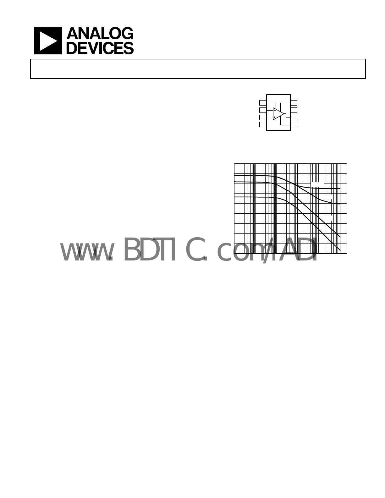
Instrumentation Amplifier
AD623
CONNECTION DIAGRAM
AD623
1
R
G
2
–IN
3
+IN
4
–V
S
TOP VIEW
(Not to Scale)
Figure 1. 8-Lead PDIP (N), SOIC (R), and MSOP (RM) Packages
120
110
100
90
80
70
CMR (dB)
60
50
40
30
1 10 100 1k 10k 100k
Figure 2. CMR vs. Frequency, 5 V
The AD623 holds errors to a minimum by providing superior
ac CMRR that increases with increasing gain. Line noise, as
well as line harmonics, are rejected because the CMRR remains
constant up to 200 Hz. The AD623 has a wide input commonmode range and can amplify signals that have a common-mode
voltage 150 mV below ground. Although the design of the AD623
was optimized to operate from a single supply, the AD623 still
provides superior performance when operated from a dual
voltage supply (±2.5 V to ±6.0 V).
Low power consumption (1.5 mW at 3 V), wide supply voltage
range, and rail-to-rail output swing make the AD623 ideal
for battery-powered applications. The rail-to-rail output stage
maximizes the dynamic range when operating from low supply
voltages. The AD623 replaces discrete instrumentation amplifier
designs and offers superior linearity, temperature stability, and
reliability in a minimum of space.
8
+R
7
+V
6
OUTPUT
5
REF
FREQUENCY (Hz)
G
S
0778-001
×1000
×100
×10
×1
00778-002
, 0 VS
S
Rev. D
Information furnished by Analog Devices is believed to be accurate and reliable. However, no
responsibility is assumed by Analog Devices for its use, nor for any infringements of patents or other
rights of third parties that may result from its use. Specifications subject to change without notice. No
license is granted by implication or otherwise under any patent or patent rights of Analog Devices.
Trademarks and registered trademarks are the property of their respective owners.
One Technology Way, P.O. Box 9106, Norwood, MA 02062-9106, U.S.A.
Tel: 781.329.4700 www.analog.com
Fax: 781.461.3113 ©1997–2008 Analog Devices, Inc. All rights reserved.

AD623
www.BDTIC.com/ADI
TABLE OF CONTENTS
Features .............................................................................................. 1
Applications ....................................................................................... 1
General Description ......................................................................... 1
Connection Diagram ....................................................................... 1
Revision History ............................................................................... 2
Specifications ..................................................................................... 3
Single Supply ................................................................................. 3
Dual Supplies ................................................................................ 4
Both Dual and Single Supplies .................................................... 6
Absolute Maximum Ratings ............................................................ 7
ESD Caution .................................................................................. 7
Typical Performance Characteristics ............................................. 8
Theory of Operation ...................................................................... 15
REVISION HISTORY
7/08—Rev. C to Rev. D
Updated Format .................................................................. Universal
Changes to Features Section and General Description Section . 1
Changes to Table 3 ............................................................................ 6
Changes to Figure 40 ...................................................................... 14
Changes to Theory of Operation Section .................................... 15
Changes to Figure 42 and Figure 43 ............................................. 16
Changes to Table 7 .......................................................................... 19
Updated Outline Dimensions ....................................................... 22
Changes to Ordering Guide .......................................................... 23
9/99—Rev. B to Rev. C
Applications Information .............................................................. 16
Basic Connection ....................................................................... 16
Gain Selection ............................................................................. 16
Reference Terminal .................................................................... 16
Input and Output Offset Voltage .............................................. 17
Input Protection ......................................................................... 17
RF Interference ........................................................................... 17
Grounding ................................................................................... 18
Input Differential and Common-Mode Range vs. Supply and
Gain .............................................................................................. 20
Outline Dimensions ....................................................................... 22
Ordering Guide .......................................................................... 23
Rev. D | Page 2 of 24
AD623
www.BDTIC.com/ADI
SPECIFICATIONS
SINGLE SUPPLY
Typical @ 25°C single supply, VS = 5 V, and RL = 10 kΩ, unless otherwise noted.
Table 1.
AD623A AD623ARM AD623B
Parameter Conditions Min Typ Max Min Typ Max Min Typ Max Unit
GAIN
Gain Range 1 1000 1 1000 1 1000
Gain Error
Nonlinearity
G = 1 to 1000 50 50 50 ppm
Gain vs. Temperature
VOLTAGE OFFSET
Input Offset, V
Output Offset, V
Offset Referred to the
INPUT CURRENT
Input Bias Current 17 25 17 25 17 25 nA
Input Offset Current 0.25 2 0.25 2 0.25 2 nA
1
G = 1 0.03 0.10 0.03 0.10 0.03 0.05 %
G = 10 0.10 0.35 0.10 0.35 0.10 0.35 %
G = 100 0.10 0.35 0.10 0.35 0.10 0.35 %
G = 1000 0.10 0.35 0.10 0.35 0.10 0.35 %
G = 1 5 10 5 10 5 10 ppm/°C
1
G > 1
50 50 50 ppm/°C
25 200 200 500 25 100 μV
OSI
Over Temperature 350 650 160 μV
Average Tempco 0.1 2 0.1 2 0.1 1 μV/°C
200 1000 500 2000 200 500 μV
OSO
Over Temperature 1500 2600 1100 μV
Average Tempco 2.5 10 2.5 10 2.5 10 μV/°C
Input vs. Supply (PSR)
G = 1 80 100 80 100 80 100 dB
G = 10 100 120 100 120 100 120 dB
G = 100 120 140 120 140 120 140 dB
G = 1000 120 140 120 140 120 140 dB
Over Temperature 27.5 27.5 27.5 nA
Average Tempco 25 25 25 pA/°C
Over Temperature 2.5 2.5 2.5 nA
Average Tempco 5 5 5 pA/°C
G =
1 + (100 k/R
G1 V
=
OUT
0.05 V to 3.5 V
G > 1 V
0.05 V to 4.5 V
G1 V
0.05 V to 3.5 V
G > 1 V
0.05 V to 4.5 V
Total RTI error =
V
=
OUT
=
OUT
=
OUT
+ V
/G
OSI
OSO
)
G
Rev. D | Page 3 of 24

AD623
www.BDTIC.com/ADI
AD623A AD623ARM AD623B
Parameter Conditions Min Typ Max Min Typ Max Min Typ Max Unit
INPUT
Input Impedance
Differential 2||2 2||2 2||2 GΩ||pF
Common-Mode 2||2 2||2 2||2 GΩ||pF
Input Voltage Range
Common-Mode Rejection
at 60 Hz with 1 kΩ Source
Imbalance
G = 1 VCM = 0 V to 3 V 70 80 70 80 77 86 dB
G = 10 VCM = 0 V to 3 V 90 100 90 100 94 100 dB
G = 100 VCM = 0 V to 3 V 105 110 105 110 105 110 dB
G = 1000 VCM = 0 V to 3 V 105 110 105 110 105 110 dB
OUTPUT
Output Swing RL = 10 kΩ 0.01
R
DYNAMIC RESPONSE
Small Signal −3 dB Bandwidth
G = 1 800 800 800 kHz
G = 10 100 100 100 kHz
G = 100 10 10 10 kHz
G = 1000 2 2 2 kHz
Slew Rate 0.3 0.3 0.3 V/μs
Settling Time to 0.01% VS = 5 V
G = 1 Step size: 3.5 V 30 30 30 μs
G = 10
1
Does not include effects of external resistor, RG.
2
One input grounded. G = 1.
2
VS = 3 V to 12 V
(−V
0.15
) −
S
(+V
1.5
) −
(−VS) −
S
0.15
(+V
1.5
) −
(−VS) −
S
0.15
(+V
V
) −
S
1.5
= 100 kΩ 0.01
L
Step size: 4 V,
= 1.8 V
V
CM
20 20 20 μs
(+V
0.5
(+V
0.15
0.01
) −
S
0.01
) −
S
(+V
0.5
(+VS) −
0.15
0.01
) −
S
0.01
) −
(+V
S
0.5
(+VS) −
0.15
V
V
DUAL SUPPLIES
Typical @ 25°C dual supply, VS = ±5 V, and RL = 10 kΩ, unless otherwise noted.
Table 2.
AD623A AD623ARM AD623B
Parameter Conditions Min Typ Max Min Typ Max Min Typ Max Unit
GAIN
G =
1 + (100 k/R
)
G
Gain Range 1 1000 1 1000 1 1000
Gain Error
1
G1 V
OUT
=
−4.8 V to +3.5 V
G > 1 V
OUT
=
0.05 V to 4.5 V
G = 1 0.03 0.10 0.03 0.10 0.03 0.05 %
G = 10 0.10 0.35 0.10 0.35 0.10 0.35 %
G = 100 0.10 0.35 0.10 0.35 0.10 0.35 %
G = 1000 0.10 0.35 0.10 0.35 0.10 0.35 %
Rev. D | Page 4 of 24

AD623
www.BDTIC.com/ADI
AD623A AD623ARM AD623B
Parameter Conditions Min Typ Max Min Typ Max Min Typ Max Unit
Nonlinearity
G1 V
OUT
=
−4.8 V to +3.5 V
G > 1 V
OUT
=
−4.8 V to +4.5 V
G = 1 to 1000 50 50 50 ppm
Gain vs. Temperature
G = 1 5 10 5 10 5 10 ppm/°C
1
G > 1
50 50 50 ppm/°C
VOLTAGE OFFSET
Input Offset, V
25 200 200 500 25 100 μV
OSI
Total RTI error =
+ V
V
/G
OSI
OSO
Over Temperature 350 650 160 μV
Average Tempco 0.1 2 0.1 2 0.1 1 μV/°C
Output Offset, V
200 1000 500 2000 200 500 μV
OSO
Over Temperature 1500 2600 1100 μV
Average Tempco 2.5 10 2.5 10 2.5 10 μV/°C
Offset Referred to the Input
vs. Supply (PSR)
G = 1 80 100 80 100 80 100 dB
G = 10 100 120 100 120 100 120 dB
G = 100 120 140 120 140 120 140 dB
G = 1000 120 140 120 140 120 140 dB
INPUT CURRENT
Input Bias Current 17 25 17 25 17 25 nA
Over Temperature 27.5 27.5 27.5 nA
Average Tempco 25 25 25 pA/°C
Input Offset Current 0.25 2 0.25 2 0.25 2 nA
Over Temperature 2.5 2.5 2.5 nA
Average Tempco 5 5 5 pA/°C
INPUT
Input Impedance
Differential 2||2 2||2 2||2 GΩ||pF
Common-Mode 2||2 2||2 2||2 GΩ||pF
Input Voltage Range
2
VS = +2.5 V to
±6 V
Common-Mode Rejection at
60 Hz with 1 kΩ Source
Imbalance
G = 1
= +3.5 V to
V
CM
−5.15 V
G = 10
= +3.5 V to
V
CM
−5.15 V
G = 100
= +3.5 V to
V
CM
−5.15 V
G = 1000
= +3.5 V to
V
CM
−5.15 V
OUTPUT
Output Swing
R
= 10 kΩ,
R
L
= ±5 V
V
S
= 100 kΩ
L
(−VS) –
0.15
(+VS) –
1.5
(−VS) –
0.15
(+VS) –
1.5
(−VS) –
0.15
(+VS) –
V
1.5
70 80 70 80 77 86 dB
90 100 90 100 94 100 dB
105 110 105 110 105 110 dB
105 110 105 110 105 110 dB
(−V
0.2
(−V
0.05
) +
S
) +
S
(+V
0.5
(+V
0.15
) −
(−VS) +
S
0.2
) −
(−VS) +
S
0.05
(+V
0.5
(+V
0.15
S
S
) −
) −
(−VS) +
0.2
(−VS) +
0.05
(+V
V
) −
S
0.5
(+V
V
) −
S
0.15
Rev. D | Page 5 of 24

AD623
www.BDTIC.com/ADI
AD623A AD623ARM AD623B
Parameter Conditions Min Typ Max Min Typ Max Min Typ Max Unit
DYNAMIC RESPONSE
Small Signal −3 dB Bandwidth
G = 1 800 800 800 kHz
G = 10 100 100 100 kHz
G = 100 10 10 10 kHz
G = 1000 2 2 2 kHz
Slew Rate 0.3 0.3 0.3 V/μs
Settling Time to 0.01%
G = 1 30 30 30 μs
G = 10 20 20 20 μs
1
Does not include effects of external resistor, RG.
2
One input grounded. G = 1.
= ±5 V,
V
S
5 V step
BOTH DUAL AND SINGLE SUPPLIES
Table 3.
AD623A AD623ARM AD623B
Parameter Conditions Min Typ Max Min Typ Max Min Typ Max Unit
NOISE
Voltage Noise, 1 kHz
Input, Voltage Noise, eni 35 35 35 nV/√Hz
Output, Voltage Noise, eno 50 50 50 nV/√Hz
RTI, 0.1 Hz to 10 Hz
G = 1 3.0 3.0 3.0 μV p-p
G = 1000 1.5 1.5 1.5 μV p-p
Current Noise f = 1 kHz 100 100 100 fA/√Hz
0.1 Hz to 10 Hz 1.5 1.5 1.5 pA p-p
REFERENCE INPUT
RIN
IIN VIN+, V
Voltage Range −VS +VS −VS +VS −VS +VS V
Gain to Output
POWER SUPPLY
Operating Range Dual supply ±2.5 ±6 ±2.5 ±6 ±2.5 ±6 V
Single supply 2.7 12 2.7 12 2.7 12 V
Quiescent Current Dual supply 375 550 375 550 375 550 μA
Single supply 305 480 305 480 305 480 μA
Over Temperature 625 625 625 μA
TEMPERATURE RANGE
For Specified Performance −40 +85 −40 +85 −40 +85 °C
Tot al RT I nois e =
2
()
()
+
no
ni
= 0 V 50 60 50 60 50 60 μA
REF
2
/Gee
100 ±
20%
1 ±
0.0002
100 ±
20%
1 ±
0.0002
100 ±
20%
1 ±
0.0002
kΩ
V
Rev. D | Page 6 of 24
AD623
www.BDTIC.com/ADI
ABSOLUTE MAXIMUM RATINGS
Table 4.
Parameter Rating
Supply Voltage ±6 V
Internal Power Dissipation
Differential Input Voltage ±6 V
Output Short-Circuit Duration Indefinite
Storage Temperature Range −65°C to +125°C
Operating Temperature Range −40°C to +85°C
Lead Temperature (Soldering, 10 sec) 300°C
1
Specification is for device in free air:
8-Lead PDIP Package: θJA = 95°C/W
8-Lead SOIC Package: θ
8-Lead MSOP Package: θ
1
650 mW
= 155°C/W
JA
= 200°C/W.
JA
Stresses above those listed under Absolute Maximum Ratings
may cause permanent damage to the device. This is a stress
rating only; functional operation of the device at these or any
other conditions above those indicated in the operational
section of this specification is not implied. Exposure to absolute
maximum rating conditions for extended periods may affect
device reliability.
ESD CAUTION
Rev. D | Page 7 of 24
AD623
www.BDTIC.com/ADI
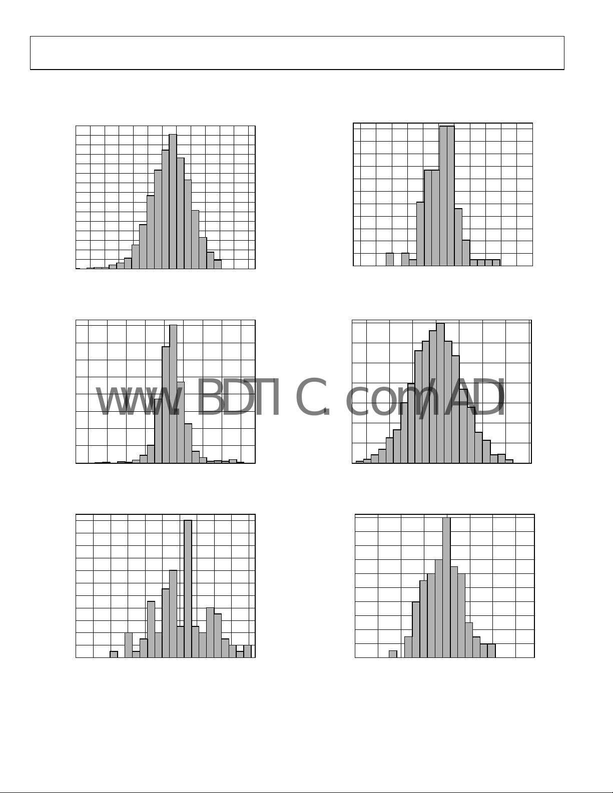
TYPICAL PERFORMANCE CHARACTERISTICS
At 25°C, VS = ±5 V, and RL = 10 kΩ, unless otherwise noted.
300
280
260
240
220
200
180
160
140
UNITS
120
100
80
60
40
20
0
–100 –80 –60 –40 –20 0 20 40 60 80 100 120 140
INPUT OFFSET VOLTAGE (µV)
00778-003
Figure 3. Typical Distribution of Input Of fset V oltage; Packa ge Option N-8, R-8
480
22
20
18
16
14
12
UNITS
10
8
6
4
2
0
–600 –500 –400 –300 –200 –100 0 100 200 300 400 500
OUTPUT OFFSET VOLTAGE (µV)
Figure 6. Typical Distribution of Output Offset Voltage, V
Single Supply, V
210
= −0.125 V; Package Option N-8, R-8
REF
= 5 V,
S
00778-006
420
360
300
240
UNITS
180
120
60
0
–800 –600 –400 –200 0 200 400 600 800
OUTPUT OFFSET VOLTAGE (µV)
00778-004
Figure 4. Typical D istribution of Output Offset Voltage; Package Opt ion N-8, R-8
22
20
18
16
14
12
UNITS
10
8
6
4
2
0
–80 –60 –40 –20 0 20 40 60 80 100
INPUT OFFSET VOLTAGE (µV)
00778-005
Figure 5. Typical Distribution of Input Offset Voltage, VS = 5 V,
Single Supply, V
= −0.125 V; Package Option N-8, R-8
REF
180
150
120
UNITS
90
60
30
0
–0.245 –0.240 –0. 235 –0.230 –0.225 –0. 220 –0. 215 –0. 210
INPUT OFF SET CURRENT (n A)
00778-007
Figure 7. Typical Distribution for Input Offset Current; Package Option N-8, R-8
20
18
16
14
12
10
UNITS
8
6
4
2
0
–0.025 –0.020 –0.015 –0.010 –0.005 0 0.005 0.010
INPUT OFF SET CURRENT (n A)
00778-008
Figure 8. Typical Distribution for Input Offset Current, VS = 5 V,
Single Supply, V
= −0.125 V; Package Option N-8, R-8
REF
Rev. D | Page 8 of 24

AD623
www.BDTIC.com/ADI
1600
30
1400
1200
1000
800
UNITS
600
400
200
0
75 13012512011511 010510095908580
CMRR (dB)
00778-009
Figure 9. Typical Distribution for CMRR (G = 1)
1k
100
G = 1
G= 10
25
20
(nA)
15
BIAS
I
10
5
0
–60 –40 –20 0 20 40 60 80 100 120 140
TEMPERATURE ( °C)
Figure 12. I
vs. Temperature
BIAS
1k
100
00778-012
G= 100
10
VOLTAGE NOISE SPECT RAL DENSITY (nV/ Hz RT I)
1 100k10k1k10010
FREQUENCY (Hz)
G= 1000
Figure 10. Voltage Noise Spectral Density vs. Frequency
22
21
20
19
(nA)
18
BIAS
I
17
16
15
14
CMV (V)
Figure 11. I
vs. CMV, VS = ±5 V
BIAS
CURRENT NOISE S PECTRAL DENSI TY (fA/ Hz)
10
1110010
00778-010
FREQUENCY (Hz)
k
00778-013
Figure 13. Current Noise Spectral Density vs. Frequency
20.0
19.5
19.0
18.5
(nA)
18.0
BIAS
I
17.5
17.0
16.5
16.0
420–2–4
00778-011
–4 201–1–2–3
Figure 14. I
CMV (V)
vs. CMV, VS = ±2.5 V
BIAS
00778-014
Rev. D | Page 9 of 24
AD623
www.BDTIC.com/ADI
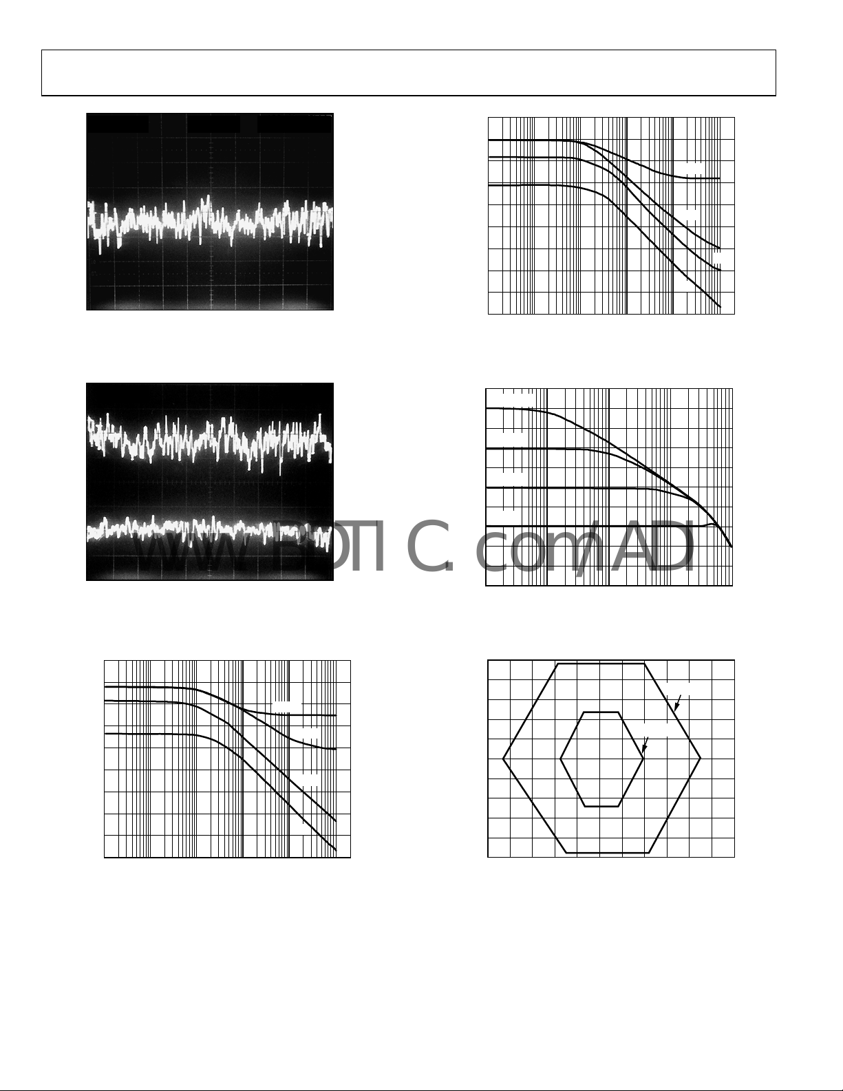
CH1 10mV A 1s 100mV VERT
Figure 15. 0.1 Hz to 10 Hz Current Noise (0.71 pA/DIV)
1µV/DIV 1s
Figure 16. 0.1 Hz to 10 Hz RTI Voltage Noise (1 DIV = 1 μV p-p)
120
110
100
90
80
70
CMR (dB)
60
50
40
30
1 10 100 1k 10k 100k
FREQUENCY (Hz)
Figure 17. CMR vs. Frequency, = 5 V
, 0 VS, V
S
×1000
×100
×10
×1
= 2.5 V
REF
00778-015
00778-016
00778-017
120
110
100
90
80
70
CMR (dB)
60
50
40
30
1 10 100 1k 10k 100k
FREQUENCY (Hz)
×1000
×100
×1
Figure 18. CMR vs. Frequency, ±5 VS
70
G = 1000
60
50
G = 100
40
30
G = 10
20
GAIN (dB)
10
G = 1
0
–10
–20
–30
100 1k 10k 100k 1M
Figure 19. Gain vs. Frequency (VS = 5 V, 0 V), V
FREQUENCY (Hz)
= 2.5 V
REF
5
4
3
2
1
0
–1
–2
–3
MAXIMUM OUTPUT VOLTAGE (V)
–4
–5
–6 –5 –4 –3 –2 –1 0 1 2 3 4 5
COMMON-MO DE INPUT (V)
V
= ±2.5V
S
VS = ±5V
Figure 20. Maximum Output Voltage vs. Common-Mode Input, G = 1, R
×10
= 100 kΩ
L
00778-018
00778-019
00778-020
Rev. D | Page 10 of 24

AD623
www.BDTIC.com/ADI
5
4
3
2
1
0
–1
–2
–3
MAXIMUM OUTPUT VOLTAGE (V)
–4
–5
–6 –5 –4 –3 –2 –1 0 1 2 3 4 5
COMMON-MO DE INPUT (V)
V
S
= ±2.5V
VS = ±5V
00778-021
Figure 21. Maximum Output Voltage vs. Common-Mode Input, G ≥ 10, RL = 100 Ω
5
140
120
100
80
60
POSITIVE PSSR (dB)
40
20
0
1 10 100 1k 10k 100k
G = 10
FREQUENCY (Hz)
G = 1000
G = 1
Figure 24. Positive PSRR vs. Frequency, ±5 V
140
G = 100
S
00778-024
4
3
2
1
MAXIMUM OUTPUT VOLTAGE (V)
0
–1012345
COMMON-MO DE INPUT (V)
Figure 22. Maximum Output Voltage vs. Common-Mode Input,
G = 1, V
= 5 V, RL = 100 kΩ
S
5
4
3
2
1
MAXIMUM OUTPUT VOLTAGE (V)
120
100
80
60
POSITIVE PSSR (dB)
40
20
0
1 10 100 1k 10k 100k
00778-022
G = 10
FREQUENCY (Hz)
Figure 25. Positive PSRR vs. Frequency, 5 V
G = 1
G = 1000
, 0 V
S
G = 100
S
00778-025
140
120
100
80
60
NEGATIVE PS RR (dB)
40
20
G = 10
G = 1000
G = 100
G = 1
0
–1012345
COMMON-MO DE INPUT (V)
Figure 23. Maximum Output Voltage vs. Common-Mode Input,
G ≥ 10, V
= 5 V, RL = 100 kΩ
S
00778-023
0
1 10 100 1k 10k 100k
Figure 26. Negative PSRR vs. Frequency, ±5 V
Rev. D | Page 11 of 24
FREQUENCY (Hz)
00778-026
S

AD623
www.BDTIC.com/ADI
10
8
6
500µV 1V 10µs
4
V
= ±2.5V
S
OUTPUT VOLTAGE (V p-p)
2
0
020
V
= ±5V
S
40 60 80 100
FREQUENCY (kHz)
Figure 27. Large Signal Response, G ≤ 10
1k
100
10
SETTLING TIME (µs)
1
1 10 100 1k
GAIN (V/V)
Figure 28. Settling Time to 0.01% vs. Gain, for a 5 V Step at Output,
= 100 pF, VS = ±5 V
C
L
00778-030
00778-027
Figure 30. Large Signal Pulse Response and Settling Time,
G = −10 (0.250 mV = 0.01%), C
10mV 2V 50µs
00778-028
= 100 pF
L
00778-031
Figure 31. Large Signal Pulse Response and Settling Time,
G = 100, C
= 100 pF
L
500µV 1V 20µs
Figure 29. Large Signal Pulse Response and Settling Time,
G = −1 (0.250 mV = 0.01%), C
= 100 pF
L
00778-029
Rev. D | Page 12 of 24
20mV 2V 500µs
Figure 32. Large Signal Pulse Response and Settling Time,
G = −1000 (5 mV = 0.01%), C
= 100 pF
L
00778-032

AD623
www.BDTIC.com/ADI
20mV 2µs
Figure 33. Small Signal Pulse Response, G = 1, R
20mV 5µs
00778-033
= 10 kΩ, CL = 100 pF
L
20mV 500µs
Figure 36. Small Signal Pulse Response, G = 1000, R
200µV
00778-036
= 10 kΩ, CL = 100 pF
L
Figure 34. Small Signal Pulse Response, G = 10, R
20mV 50µs
Figure 35. Small Signal Pulse Response, G = 100, R
00778-034
= 10 kΩ, CL = 100 pF
L
00778-035
= 10 kΩ, CL = 100 pF
L
1V
Figure 37. Gain Nonlinearity, G = −1 (50 ppm/DIV)
20µV 1V
Figure 38. Gain Nonlinearity, G = −10 (6 ppm/DIV)
0778-037
00778-038
Rev. D | Page 13 of 24

AD623
V
www.BDTIC.com/ADI
50µV 1V
00778-039
Figure 39. Gain Nonlinearity, G = −100, 15 ppm/DIV
+
(V+) –0.5
(V+) –1.5
(V+) –2.5
OUTPUT VOLTAGE SWING (V)
(V–) +0.5
V–
0 0.5 1.0 1.5 2.0
Figure 40. Output Voltage Swing vs. Output Current
OUTPUT CURRENT (mA)
00778-040
Rev. D | Page 14 of 24

AD623
www.BDTIC.com/ADI
THEORY OF OPERATION
The AD623 is an instrumentation amplifier based on a modified
classic 3-op-amp approach, to assure single or dual supply
operation even at common-mode voltages at the negative
supply rail. Low voltage offsets, input and output, as well as
absolute gain accuracy, and one external resistor to set the
gain, make the AD623 one of the most versatile instrumentation
amplifiers in its class.
The input signal is applied to PNP transistors acting as voltage
buffers and providing a common-mode signal to the input
amplifiers (see Figure 41). An absolute value 50 kΩ resistor in
each amplifier feedback assures gain programmability.
The differential output is
⎛
⎜
+=
1
V
O
⎜
⎝
⎞
k100
⎟
V
C
⎟
R
G
⎠
The differential voltage is then converted to a single-ended
voltage using the output amplifier, which also rejects any
common-mode signal at the output of the input amplifiers.
Because the amplifiers can swing to either supply rail, as well as
have their common-mode range extended to below the negative
supply rail, the range over which the AD623 can operate is further
enhanced (see Figure 20 and Figure 21).
The output voltage at Pin 6 is measured with respect to the
potential at Pin 5. The impedance of the reference pin is 100 kΩ;
therefore, in applications requiring V/I conversion, a small
resistor between Pin 5 and Pin 6 is all that is needed.
POSITIVE SUPPLY
7
INVERTING
2
4
1
GAIN
8
NONINVERTING
3
NEGATIVE SUPPLY
50kΩ
50kΩ
7
4
Figure 41. Simplified Schematic
50kΩ 50kΩ
50kΩ 50kΩ
OTUPUT
6
REF
5
00778-041
Note that the bandwidth of the in-amp decreases as gain is
increased. This occurs because the internal op-amps are the
standard voltage feedback design. At unity gain, the output
amplifier limits the bandwidth.
Rev. D | Page 15 of 24

AD623
V
V
www.BDTIC.com/ADI
APPLICATIONS INFORMATION
BASIC CONNECTION
Figure 42 and Figure 43 show the basic connection circuits for
the AD623. The +V
power supply. The supply can be either bipolar (V
±6 V) or single supply (−V
supplies should be capacitively decoupled close to the power pins of
the device. For the best results, use surface-mount 0.1 µF ceramic
chip capacitors and 10 µF electrolytic tantalum capacitors.
and −VS terminals are connected to the
S
= 0 V, +VS = 3.0 V to 12 V). Power
S
+
S
10µF0.1µF
+2.5V TO +6V
R
V
IN
Figure 42. Dual-Supply Basic Connection
V
IN
OUTPUT
G
REF
R
G
10µF0.1µF
–V
S
–2.5V TO –6V
+
S
10µF0.1µF
+3V TO +12V
R
G
R
OUTPUT
G
REF
R
G
G
R
V
OUT
REF (INPUT)
V
OUT
REF (INPUT)
= ±2.5 V to
S
00778-042
The input voltage, which can be either single-ended (tie either
−IN or +IN to ground), or differential is amplified by the
programmed gain. The output signal appears as the voltage
difference between the OUTPUT pin and the externally applied
voltage on the REF input. For a ground-referenced output, REF
should be grounded.
GAIN SELECTION
The gain of the AD623 is resistor programmed by RG, or more
precisely, by whatever impedance appears between Pin 1 and
Pin 8. The AD623 is designed to offer accurate gains using 0.1%
to 1% tolerance resistors. Table 5 shows the required values of
for the various gains. Note that for G = 1, the RG terminals
R
G
are unconnected (R
= ∞). For any arbitrary gain, RG can be
G
calculated by
R
= 100 kΩ/(G − 1)
G
REFERENCE TERMINAL
The reference terminal potential defines the zero output voltage
and is especially useful when the load does not share a precise
ground with the rest of the system. It provides a direct means of
injecting a precise offset to the output. The reference terminal is
also useful when bipolar signals are being amplified because it
can be used to provide a virtual ground voltage. The voltage on
the reference terminal can be varied from −V
to +VS.
S
00778-055
Figure 43. Single-Supply Basic Connection
Table 5. Required Values of Gain Resistors
Desired Gain 1% Standard Table Value of RG (Ω) Calculated Gain Using 1% Resistors
2 100 k 2
5 24.9 k 5.02
10 11 k 10.09
20 5.23 k 20.12
33 3.09 k 33.36
40 2.55 k 40.21
50 2.05 k 49.78
65 1.58 k 64.29
100 1.02 k 99.04
200 499 201.4
500 200 501
1000 100 1001
Rev. D | Page 16 of 24

AD623
V
V
www.BDTIC.com/ADI
INPUT AND OUTPUT OFFSET VOLTAGE
The low errors of the AD623 are attributed to two sources,
input and output errors. The output error is divided by the
programmed gain when referred to the input. In practice,
the input errors dominate at high gains and the output errors
dominate at low gains. The total V
for a given gain is calculated
OS
as the following:
Total Error RTI = Input Error + (Output Error/G)
Total Error RTO = (Input Error × G) + Output Error
RTI offset errors and noise voltages for different gains are
shown in Tab l e 6.
INPUT PROTECTION
Internal supply referenced clamping diodes allow the input,
reference, output, and gain terminals of the AD623 to safely
withstand overvoltages of 0.3 V above or below the supplies.
This is true for all gains and for power on and power off. This
last case is particularly important because the signal source
and amplifier may be powered separately.
If the overvoltage is expected to exceed this value, the current
through these diodes should be limited to about 10 mA using
external current limiting resistors (see Figure 44). The size of
this resistor is defined by the supply voltage and the required
overvoltage protection.
+
S
I = 10mA MAX
V
V
OVER
OVER
R
LIM
R
G
R
LIM
Figure 44. Input Protection
–V
S
AD623
R
=
LIM
V
OVER
OUTPUT
–VS + 0.7V
10mA
00778-043
RF INTERFERENCE
All instrumentation amplifiers can rectify high frequency out-
of-band signals. Once rectified, these signals appear as dc offset
errors at the output. The circuit in Figure 45 provides good RFI
suppression without reducing performance within the pass band of
the in-amp. Resistor R1 and Capacitor C1 (and likewise, R2 and
C2) form a low-pass RC filter that has a −3 dB bandwidth equal
F = 1/(2 π R1C1). Using the component values shown, this
to
filter has a −3 dB bandwidth of approximately 40 kHz. Resistors
R1 and R2 were selected to be large enough to isolate the input of
the circuit from the capacitors, but not large enough to significantly
increase the noise of the circuit. To preserve common-mode rejection
in the amplifier’s pass band, Capacitors C1 and C2 need to be 5%
or better units, or low cost 20% units can be tested and binned
to provide closely matched devices.
+
S
0.01µF0.33µF
1000pF
5%
0.047µF
1000pF
5%
C1
C3
C2
R
AD623
G
0.01µF0.33µF
+V
S
REFERENCE
V
OUT
00778-044
R1
4.02kΩ
1%
–IN
R2
4.02kΩ
1%
+IN
NOTES:
1. LOCATE C1 TO C3 AS CLO SE TO T HE INPUT PI NS AS POSSI BLE.
Figure 45. Circuit to Attenuate RF Interference
Capacitor C3 is needed to maintain common-mode rejection at
the low frequencies. R1/R2 and C1/C2 form a bridge circuit whose
output appears across the input pins of the in-amp. Any mismatch
between C1 and C2 unbalances the bridge and reduces the
common-mode rejection. C3 ensures that any RF signals are
common mode (the same on both in-amp inputs) and are not
applied differentially. This second low-pass network, R1 + R2 and
C3, has a −3 dB frequency equal to 1/(2 π (R1 + R2) (C3)). Using a
C3 value of 0.047 µF, the −3 dB signal bandwidth of this circuit is
approximately 400 Hz. The typical dc offset shift over frequency is
less than 1.5 µV and the circuit’s RF signal rejection is better than
71 dB. The 3 dB signal bandwidth of this circuit may be increased
to 900 Hz by reducing Resistors R1 and R2 to 2.2 kΩ. The
performance is similar to using 4 kΩ resistors, except that the
circuitry preceding the in-amp must drive a lower impedance load.
Table 6. RTI Error Sources
Maximum Total Input Offset Error (μV) Maximum Total Input Offset Drift (μV/°C) Total Input Referred Noise (nV/√Hz)
Gain AD623A AD623B AD623A AD623B AD623A and AD623B
1 1200 600 12 11 62
2 700 350 7 6 45
5 400 200 4 3 38
10 300 150 3 2 35
20 250 125 2.5 1.5 35
50 220 110 2.2 1.2 35
100 210 105 2.1 1.1 35
1000 200 100 2 1 35
Rev. D | Page 17 of 24

AD623
V
www.BDTIC.com/ADI
The circuit in Figure 45 should be built using a PC board with a
ground plane on both sides. All component leads should be as
short as possible. Resistors R1 and R2 can be common 1% metal
film units, but Capacitors C1 and C2 need to be ±5% tolerance
devices to avoid degrading the circuit’s common-mode rejection.
Either the traditional 5% silver mica units or Panasonic ±2%
PPS film capacitors are recommended.
In many applications, shielded cables are used to minimize
noise; for best CMR over frequency, the shield should be properly
driven. Figure 46 shows an active guard driver that is configured
to improve ac common-mode rejection by bootstrapping the
capacitances of input cable shields, thus minimizing the capacitance
mismatch between the inputs.
+
S
100Ω
–IN
AD8031
+IN
2
R
1
G
2
R
G
8
2
3
AD623
4
–V
S
7
6
OUTPUT
5
REF
Figure 46. Common-Mode Shield Driver
GROUNDING
Because the AD623 output voltage is developed with respect to
the potential on the reference terminal, many grounding problems
can be solved by simply tying the REF pin to the appropriate local
0778-045
ground. The REF pin should, however, be tied to a low impedance
point for optimal CMR.
The use of ground planes is recommended to minimize the
impedance of ground returns (and hence the size of dc errors).
To isolate low level analog signals from a noisy digital environment,
many data acquisition components have separate analog and
digital ground returns (see Figure 47). All ground pins from
mixed signal components, such as analog-to-digital converters
(ADCs), should be returned through the high quality analog
ground plane. Maximum isolation between analog and digital is
achieved by connecting the ground planes back at the supplies.
The digital return currents from the ADC that flow in the analog
ground plane, in general, have a negligible effect on noise
performance.
If there is only a single power supply available, it must be shared
by both digital and analog circuitry. Figure 48 shows how to
minimize interference between the digital and analog circuitry.
As in the previous case, separate analog and digital ground planes
should be used (reasonably thick traces can be used as an
alternative to a digital ground plane). These ground planes
should be connected at the ground pin of the power supply.
Separate traces should be run from the power supply to the
supply pins of the digital and analog circuits. Ideally, each device
should have its own power supply trace, but these can be shared
by a number of devices, as long as a single trace is not used to
route current to both digital and analog circuitry.
ANALOG POW ER SUPPLY
GND–5V+5V
2
3
7
AD623
4
6
5
1
6
V
AGND14DGND
DD
4
V
IN1
3
V
IN2
ADC
AD7892-2
Figure 47. Optimal Grounding Practice for a Bipolar Supply Environment with Separate Analog and Digital Supplies
POWER SUPPLY
+5V GND
0.1µF
1
6
V
AGND14DGND
DD
4
V
IN1
ADC
AD7892-2
2
3
7
AD623
0.1µF
4
6
5
Figure 48. Optimal Ground Practice in a Single Supply Environment
DIGITAL POWER SUPPLY
0.1µF0.1µF0.1µF 0.1µ F
AGND V
12
MICROPROCESSOR
0.1µF
AGND V
12
MICROPROCESSOR
+5VGND
DD
0778-046
DD
0778-047
Rev. D | Page 18 of 24

AD623
V
V
V
V
V
www.BDTIC.com/ADI
Ground Returns for Input Bias Currents
Input bias currents are those dc currents that must flow to bias
the input transistors of an amplifier. These are usually transistor
base currents. When amplifying floating input sources, such as
transformers or ac-coupled sources, there must be a direct dc
path into each input in order that the bias current can flow.
Figure 49, Figure 50, and Figure 51 show how a bias current
path can be provided for the cases of transformer coupling,
thermocouple, and capacitive ac coupling. In dc-coupled resistive
bridge applications, providing this path is generally not necessary
as the bias current simply flows from the bridge supply through
the bridge into the amplifier. However, if the impedances that
the two inputs see are large and differ by a large amount (>10 kΩ),
the offset current of the input stage causes dc errors
proportional with the input offset voltage of the amplifier.
+
AD623
4
–V
S
S
7
6
5
REF
LOAD
OUTPUT
TO POWER
SUPPLY
GROUND
00778-048
–IN
2
1
R
G
8
3
+IN
Figure 49. Ground Returns for Bias Currents with Transformer-Coupled Inputs
+
AD623
4
–V
S
S
7
6
5
REF
LOAD
OTUPUT
TO POWER
SUPPLY
GROUND
00778-049
–IN
2
1
R
G
8
3
+IN
Figure 50. Ground Returns for Bias Currents with Thermocouple Inputs
+
AD623
4
–V
S
S
7
6
5
REF
LOAD
OUTPUT
TO POWER
SUPPLY
GROUND
00778-050
100kΩ
R
100kΩ
–IN
2
1
G
8
3
+IN
Figure 51. Ground Returns for Bias Currents with AC-Coupled Inputs
Output Buffering
The AD623 is designed to drive loads of 10 kΩ or greater. If
the load is less than this value, the output of the AD623 should
be buffered with a precision single-supply op amp, such as the
OP113. This op amp can swing from 0 V to 4 V on its output
while driving a load as small as 600 Ω. Ta b le 7 summarizes the
performance of some buffer op amps.
5
0.1µF
V
R
G
AD623
REFERENCE
IN
5V
OP113
0.1µF
V
OUT
00778-051
Figure 52. Output Buffering
Table 7. Buffering Options
Op Amp Description
OP113 Single supply, high output current
OP191 Rail-to-rail input and output, low supply current
Single-Supply Data Acquisition System
Interfacing bipolar signals to single-supply ADCs presents a
challenge. The bipolar signal must be mapped into the input
range of the ADC. Figure 53 shows how this translation can be
achieved.
5V
±10mV
1.02kΩ
5V
0.1µF
R
G
AD623
REFERENCE
Figure 53. A Single-Supply Data Acquisition System
5
AD7776
A
IN
REFOUT
REFIN
0.1µF
The bridge circuit is excited by a 5 V supply. The full-scale output
voltage from the bridge (±10 mV) therefore has a commonmode level of 2.5 V. The AD623 removes the common-mode
component and amplifies the input signal by a factor of 100
= 1.02 kΩ). This results in an output signal of ±1 V. To
(R
GAIN
prevent this signal from running into the ground rail of the
AD623, the voltage on the REF pin must be raised to at least
1 V. In this example, the 2 V reference voltage from the AD7776
ADC is used to bias the output voltage of the AD623 to 2 V ± 1 V.
This corresponds to the input range of the ADC.
00778-052
Rev. D | Page 19 of 24

AD623
V
T
T
T
www.BDTIC.com/ADI
Amplifying Signals with Low Common-Mode Voltage
Because the common-mode input range of the AD623 extends
0.1 V below ground, it is possible to measure small differential
signals which have low, or no, common-mode component.
Figure 54 shows a thermocouple application where one side
of the J-type thermocouple is grounded.
5
0.1µF
J-TYPE
HERMOCOUPLE
1.02kΩ
R
G
AD623
REF
OUTPU
2V
00778-053
Figure 54. Amplifying Bipolar Signals with Low Common-Mode Voltage
Over a temperature range of −200°C to +200°C, the J-type thermocouple delivers a voltage ranging from −7.890 mV to +10.777 mV.
A programmed gain on the AD623 of 100 (R
= 1.02 kΩ) and a
G
voltage on the REF pin of 2 V, results in the output voltage ranging
from 1.110 V to 3.077 V relative to ground.
INPUT DIFFERENTIAL AND COMMON-MODE RANGE vs. SUPPLY AND GAIN
Figure 55 shows a simplified block diagram of the AD623. The
voltages at the outputs of Amplifier A1 and Amplifier A2 are
given by
V
= VCM + V
A2
= VCM + 0.6 V + V
V
= VCM + V
A1
= VCM + 0.6 V − V
INVERTING
2
–
V
DIFF
2
+
V
CM
–
V
DIFF
2
+
NONINVERTI NG
3
NEGATIVE SUPPLY
The voltages on these internal nodes are critical in determining
whether the output voltage will be clipped. The V
voltages can swing from approximately 10 mV above the negative
supply (V− or ground) to within approximately 100 mV of the
positive rail before clipping occurs. Based on this and from
/2 + 0.6 V + V
DIFF
/2 + 0.6 V + V
DIFF
POSITIVE SUPPLY
7
4
GAIN
R
G
7
4
DIFF
DIFF
1
8
× Gain/2
× Gain/2
50kΩ
50kΩ
A1
R
R
A2
F
F
× RF/R
DIFF
× RF/R
DIFF
50kΩ 50kΩ
50kΩ 50kΩ
Figure 55. Simplified Block Diagram
G
G
and VA2
OUTPU
6
REF
5
A3
A1
00778-054
the previous equations, the maximum and minimum input
common-mode voltages are given by the following equations:
V
= V+ − 0.7 V − V
CMMAX
V
= V− − 0.590 V + V
CMMIN
× Gain/2
DIFF
× Gain/2
DIFF
These equations can be rearranged to give the maximum
possible differential voltage (positive or negative) for a
particular common-mode voltage, gain, and power supply.
Because the signals on A1 and A2 can clip on either rail, the
maximum differential voltage are the lesser of the two equations.
V
|
|
| = 2 (V+ − 0.7 V − VCM/Gain
DIFFMAX
V
| = 2 (VCM − V− +0.590 V/Gain
DIFFMAX
However, the range on the differential input voltage range is
also constrained by the output swing. Therefore, the range of
may have to be lower according the following equation.
V
DIFF
Input Range ≤ Available Output Swing/Gain
For a bipolar input voltage with a common-mode voltage that is
roughly half way between the rails, V
is half the value that
DIFFMAX
the previous equations yield because the REF pin is at midsupply.
Note that the available output swing is given for different supply
conditions in the Specifications section.
The equations can be rearranged to give the maximum gain for
a fixed set of input conditions. Again, the maximum gain will be
the lesser of the two equations.
Gain
Gain
= 2 (V+ − 0.7 V − VCM)/V
MAX
= 2 (VCM − V− +0.590 V)/V
MAX
DIFF
DIFF
Again, it is recommended that the resulting gain times the input
range is less than the available output swing. If this is not the
case, the maximum gain is given by
Gain
Also for bipolar inputs (that is, input range = 2 V
= Available Output Swing/Input Range
MAX
DIFF
), the
maximum gain is half the value yielded by the previous equations
because the REF pin must be at midsupply.
The maximum gain and resulting output swing for different
input conditions is given in Tab l e 8 . Output voltages are
referenced to the voltage on the REF pin.
For the purposes of computation, it is necessary to break down the
input voltage into its differential and common-mode component.
Therefore, when one of the inputs is grounded or at a fixed
voltage, the common-mode voltage changes as the differential
voltage changes. Take the case of the thermocouple amplifier
in Figure 54. The inverting input on the AD623 is grounded;
therefore, when the input voltage is −10 mV, the voltage on the
noninverting input is −10 mV. For the purpose of the signal swing
calculations, this input voltage should be composed of a commonmode voltage of −5 mV (that is, (+IN + −IN)/2) and a differential
input voltage of −10 mV (that is, +IN − −IN).
Rev. D | Page 20 of 24

AD623
www.BDTIC.com/ADI
Table 8. Maximum Attainable Gain and Resulting Output Swing for Different Input Conditions
Closest 1% Gain
VCM (V) V
0 ±10 m 2.5 +5 118 866 116 ±1.2
0 ±100 m 2.5 +5 11.8 9.31 k 11.7 ±1.1
0 ±10 m 0 ±5 490 205 488 ±4.8
0 ±100 m 0 ±5 49 2.1 k 48.61 ±4.8
0 ±1 0 ±5 4.9 26.1 k 4.83 ±4.8
2.5 ±10 m 2.5 +5 242 422 238 ±2.3
2.5 ±100 m 2.5 +5 24.2 4.32 k 24.1 ±2.4
2.5 ±1 2.5 +5 2.42 71.5 k 2.4 ±2.4
1.5 ±10 m 1.5 +3 142 715 141 ±1.4
1.5 ±100 m 1.5 +3 14.2 7.68 k 14 ±1.4
0 ±10 m 1.5 +3 118 866 116 ±1.1
0 ±100 m 1.5 +3 11.8 9.31 k 11.74 ±1.1
(V) REF Pin (V) Supply Voltages (V) Maximum Gain
DIFF
Resistor (Ω) Resulting Gain Output Swing (V)
Rev. D | Page 21 of 24

AD623
www.BDTIC.com/ADI
OUTLINE DIMENSIONS
0.400 (10.16)
0.365 (9.27)
0.355 (9.02)
0.210 (5.33)
0.150 (3.81)
0.130 (3.30)
0.115 (2.92)
0.022 (0.56)
0.018 (0.46)
0.014 (0.36)
MAX
8
1
0.100 (2.54)
0.070 (1.78)
0.060 (1.52)
0.045 (1.14)
BSC
5
4
0.280 (7.11)
0.250 (6.35)
0.240 (6.10)
0.015
(0.38)
MIN
SEATING
PLANE
0.005 (0.13)
MIN
0.060 (1.52)
MAX
0.015 (0.38)
GAUGE
PLANE
0.325 (8.26)
0.310 (7.87)
0.300 (7.62)
0.430 (10.92)
MAX
0.195 (4.95)
0.130 (3.30)
0.115 (2.92)
0.014 (0.36)
0.010 (0.25)
0.008 (0.20)
CONTROLL ING DIMENS IONS ARE IN INCHES; MILLIMETER DI MENSIONS
(IN PARENTHESES) ARE ROUNDED-OF F INCH EQUI VALENTS FOR
REFERENCE ONLY AND ARE NOT APPROPRI ATE FOR USE IN DESIGN.
CORNER LEADS MAY BE CONFIGURED AS WHOL E OR HALF LEADS.
COMPLIANT TO JEDEC STANDARDS MS-001
070606-A
Figure 56. 8-Lead Plastic Dual In-Line Package [PDIP]
Narrow Body (N-8)
Dimensions shown in inches and (millimeters)
5.00 (0.1968)
4.80 (0.1890)
4.00 (0.1574)
3.80 (0.1497)
0.25 (0.0098)
0.10 (0.0040)
COPLANARITY
0.10
CONTROLL ING DIMENSI ONS ARE IN MILLIMETERS; INCH DI MENSIONS
(IN PARENTHESES) ARE ROUNDED-OFF MILLIMETER EQUIVALENTS FOR
REFERENCE ONLY AND ARE NOT APPROPRI ATE FOR USE IN DESIGN.
85
1
1.27 (0.0500)
SEATING
PLANE
COMPLIANT TO JEDEC STANDARDS MS-012-A A
BSC
6.20 (0.2441)
5.80 (0.2284)
4
1.75 (0.0688)
1.35 (0.0532)
0.51 (0.0201)
0.31 (0.0122)
8°
0°
0.25 (0.0098)
0.17 (0.0067)
0.50 (0.0196)
0.25 (0.0099)
1.27 (0.0500)
0.40 (0.0157)
45°
012407-A
Figure 57. 8-Lead Standard Small Outline Package [SOIC_N]
Narrow Body (R-8)
Dimensions shown in millimeters and (inches)
Rev. D | Page 22 of 24

AD623
www.BDTIC.com/ADI
0.95
0.85
0.75
0.15
0.00
COPLANARITY
3.20
3.00
2.80
8
5
4
SEATING
PLANE
5.15
4.90
4.65
1.10 MAX
0.23
0.08
3.20
3.00
1
2.80
PIN 1
0.65 BSC
0.38
0.22
0.10
COMPLIANT TO JEDEC STANDARDS MO-187-AA
8°
0°
0.80
0.60
0.40
Figure 58. 8-Lead Mini Small Outline Package [MSOP]
(RM-8)
Dimensions shown in millimeters
ORDERING GUIDE
Te mp e ra tu r e
Model
Range
Package Description
AD623AN −40°C to +85°C 8-Lead Plastic Dual In-Line Package [PDIP] N-8
AD623ANZ
1
−40°C to +85°C 8-Lead Plastic Dual In-Line Package [PDIP] N-8
AD623AR −40°C to +85°C 8-Lead Standard Small Outline Package [SOIC_N] R-8
AD623AR-REEL −40°C to +85°C 8-Lead Standard Small Outline Package [SOIC_N], 13" Tape and Reel R-8
AD623AR-REEL7 −40°C to +85°C 8-Lead Standard Small Outline Package [SOIC_N], 7" Tape and Reel R-8
AD623ARZ
AD623ARZ-R7
AD623ARZ-RL
1
−40°C to +85°C 8-Lead Standard Small Outline Package [SOIC_N] R-8
1
−40°C to +85°C 8-Lead Standard Small Outline Package [SOIC_N], 7" Tape and Reel R-8
1
−40°C to +85°C 8-Lead SOIC, 13" Tape and Reel R-8
AD623ARM −40°C to +85°C 8-Lead Mini Small Outline Package [MSOP] RM-8 J0A
AD623ARM-REEL −40°C to +85°C 8-Lead Mini Small Outline Package [MSOP], 13" Tape and Reel RM-8 J0A
AD623ARM-REEL7 −40°C to +85°C 8-Lead Mini Small Outline Package [MSOP], 7" Tape and Reel RM-8 J0A
AD623ARMZ
AD623ARMZ-REEL
AD623ARMZ-REEL7
1
−40°C to +85°C 8-Lead Mini Small Outline Package [MSOP] RM-8 J0A
1
−40°C to +85°C 8-Lead Mini Small Outline Package [MSOP], 13" Tape and Reel RM-8 J0A
1
−40°C to +85°C 8-Lead Mini Small Outline Package [MSOP], 7" Tape and Reel RM-8 J0A
AD623BN −40°C to +85°C 8-Lead Plastic Dual In-Line Package [PDIP] N-8
AD623BNZ
1
−40°C to +85°C 8-Lead Plastic Dual In-Line Package [PDIP] N-8
AD623BR −40°C to +85°C 8-Lead Standard Small Outline Package [SOIC_N] R-8
AD623BR-REEL −40°C to +85°C 8-Lead Standard Small Outline Package [SOIC_N], 13" Tape and Reel R-8
AD623BR-REEL7 −40°C to +85°C 8-Lead Standard Small Outline Package [SOIC_N], 7" Tape and Reel R-8
AD623BRZ
AD623BRZ-R7
AD623BRZ-RL
EVAL-INAMP-62RZ
1
Z = RoHS Compliant Part.
1
−40°C to +85°C 8-Lead Standard Small Outline Package [SOIC_N] R-8
1
−40°C to +85°C 8-Lead Standard Small Outline Package [SOIC_N], 7" Tape and Reel R-8
1
−40°C to +85°C 8-Lead Standard Small Outline Package [SOIC_N], 13" Tape and Reel R-8
1
Evaluation Board
Package
Option
Branding
Rev. D | Page 23 of 24

AD623
www.BDTIC.com/ADI
NOTES
©1997–2008 Analog Devices, Inc. All rights reserved. Trademarks and
registered trademarks are the property of their respective owners.
D00788-0-7/08(D)
Rev. D | Page 24 of 24
 Loading...