Analog Devices AD6190 Datasheet

a
900 MHz RF Transceiver
AD6190
FEATURES
Complete 900 MHz RF Transceiver
LNA
Receive Mixer
Transmit Mixer
Driver Amplifier
VCO
Prescaler
Limiter Amplifier with RSSI
On-Chip Low Dropout Regulator
Independent Sleep Modes for TX, RX
28-Lead SSOP Package
APPLICATIONS
902 MHz–928 MHz ISM Band Cordless Telephones
902 MHz–928 MHz ISM Band Wireless Data Systems
GENERAL DESCRIPTION
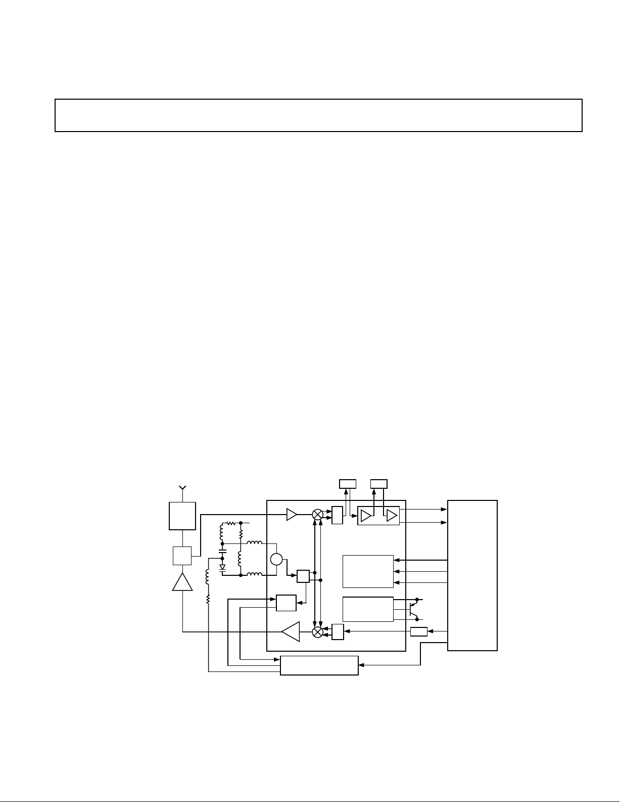
The AD6190 900 MHz RF Transceiver provides a complete
RF/IF section for systems operating in the 902 MHz–928 MHz
license-free ISM band. The high level of integration allows several
dozen discrete components to be replaced. It is ideally suited
for use in cordless telephone and wireless data applications.
The receiver section includes a Low Noise Amplifier (LNA).
The LNA’s output drives an image-reject mixer; the mixer’s
output optimized for 10.7 MHz is filtered and processed by the
limiting IF amplifier.
The transmit section accepts a modulated 10.7 MHz IF input,
and uses an image-reject upconverter to mix the signal up to the
902 MHz–928 MHz RF carrier frequency while suppressing the
unwanted image and LO components. The RF output is raised
to a nominal 0.5 milliwatt (–3 dBm) output level. This output
can be used directly or can drive an external power amplifier to
higher levels.
The on-chip VCO operates at 2× the local oscillator frequency.
This reduces oscillator pulling due to strong interferers in-band
or transmitter leakage. An on-chip 64/65 prescaler allows the
VCO to be controlled by a low cost 15 MHz CMOS synthesizer.
An on-chip low dropout regulator minimizes VCO pushing. The
transmit section, receive section, or both, can be placed in a low
current SLEEP mode when not in use. The AD6190 900 MHz
RF transceiver is packaged in a 28-lead SSOP package.
The AD6190 900 MHz RF Transceiver is part of the Analog
Devices/Zilog “A-to-Z Phone” Spread-Spectrum System for
cordless telephone and data communications applications. Contact Zilog directly at (408) 370-8000 for more information on
the Z87000 series baseband controller chips.
FUNCTIONAL BLOCK DIAGRAM
ANT
FILTER
T/R
S/W
PA
VREG
VCO
/2
64/65
15MHz SYNTHESIZER
REV. 0
Information furnished by Analog Devices is believed to be accurate and
reliable. However, no responsibility is assumed by Analog Devices for its
use, nor for any infringements of patents or other rights of third parties
which may result from its use. No license is granted by implication or
otherwise under any patent or patent rights of Analog Devices.
10.7 10.7
0
90
AD6190
POWER
MANAGEMENT
AND
IQ
CONTROL
VOLTAGE
REGULATOR
0
90
One Technology Way, P.O. Box 9106, Norwood, MA 02062-9106, U.S.A.
Tel: 781/329-4700 World Wide Web Site: http://www.analog.com
Fax: 781/326-8703 © Analog Devices, Inc., 1998
RSSI
LIMOUT
TXON
RXON
VCOON
VBATT
VREG
10.7
Z87L00
SPREAD-
SPECTRUM
CONTROLLER

(@ TA = +258C, VCC = +3.3 V, FIF = 10.7 MHz, FRF = 902 MHz–928 MHz, TX IF Input
AD6190–SPECIFICA TIONS
Parameter Conditions Min Typ Max Units
RECEIVE RF SECTION
(LNA to Mixer Output) Source Z = 50 Ω, IF Load Z = 330 Ω
Power Gain 24 dB
Noise Figure 4.2 dB
1 dB Compression (Input) –30 dBm
Input IP3 –17 dBm
Image Rejection FRF = 915 MHz, F
TRANSMIT UPCONVERTER
Image Rejection F
LO Feedthrough FIF = 10.7 MHz, FLO = 904.3 MHz –33 dBm
DRIVER AMPLIFIER
Nominal Output Power For IF Input Level = 137 mV p-p –3 dBm
1 dB Compression 0 +4.5 dBm
VCO
Operating Frequency (LO Frequency ×2) 1783 1835 MHz
PRESCALER
Division Ratio
PREMOD = “1” 64
PREMOD = “0” 65
Output Level RL = 2.2 k, CL < 10 pF 0.55 1.0 V p-p
IF LIMITER AMPLIFIER
First Stage Gain 24 dB
Second Stage Gain 70 dB
AC Output Level R
DC Level 1.76 V
IF Port Impedance FIF = 10.7 MHz 330 Ω
RSSI OUTPUT
Slope With 10 Ω in Series with VCCIF 22 mV/dB
Output Voltage @ –100 dBm RF Input 0.90 V
Linear Range (With Respect to RF Input Level) 70 dB
RSSI Log Conformance Error ±2dB
SUPPLY CURRENT (VCC = 3.3 V)
Transmit Mode TXON, VCOON = 1; RXON = 0 93 mA
Receive Mode RXON, VCOON = 1; TXON = 0 59 mA
Sleep Mode TXON, VCOON, RXON = 0 270 µA
SUPPLY VOLTAGE VBATT 3.0 4.6 V
Other Supplies VCCTX, VCCIF, VCCLNA 3.0 3.3 3.6 V
VCO REGULATOR Output Voltage, 3.0 < VBATT < 4.6 V 2.65 2.85 V
TEMPERATURE RANGE –20 +85 °C
Specifications subject to change without notice.
= 10.7 MHz, F
IF
> 30 kΩ, CL < 30 pF 450 mV p-p
L
@ –30 dBm RF Input 2.40 V
level 137 mV p-p, unless otherwise noted)
= 904.3 MHz 28 33 dBc
LO
= 904.3 MHz 35 48 dBc
LO
–2–
REV. 0

AD6190
ABSOLUTE MAXIMUM RATINGS
1
Supply Voltage
VBATT, VCCIF, LNAVCC, VCCTX to GND . . . .+5.5 V
Maximum RF Input Level Without Damage . . . . . . .+20 dBm
Internal Power Dissipation
2
. . . . . . . . . . . . . . . . . . . . 500 mW
Operating Temperature Range . . . . . . . . . . . –25°C to +85°C
NOTES
1
Stresses above those listed under Absolute Maximum Ratings may cause perma-
nent damage to the device. This is a stress rating only; functional operation of the
device at these or any other conditions above those indicated in the operational
section of this specification is not implied. Exposure to absolute maximum rating
conditions for extended periods may affect device reliability.
2
Thermal Characteristics: 28-lead SSOP package θJA = 122°C/W.
Storage Temperature Range . . . . . . . . . . . . –65°C to +150°C
Lead Temperature Range
(Soldering, 60 sec) . . . . . . . . . . . . . . . . . . . . . . . . . . +300°C
ORDERING GUIDE
Model Package Description Package Option
AD6190ARS 28-Lead Shrink Small Outline RS-28
AD6190ARSRL 28-Lead Shrink Small Outline, Supplied on Reels, 1500 Units per Reel
Minimum order quantity 25,000 units.
CAUTION
ESD (electrostatic discharge) sensitive device. Electrostatic charges as high as 4000 V readily
accumulate on the human body and test equipment and can discharge without detection.
WARNING!
Although the AD6190 features proprietary ESD protection circuitry, permanent damage
may occur on devices subjected to high energy electrostatic discharges. Therefore,
proper ESD precautions are recommended to avoid performance degradation or loss of
ESD SENSITIVE DEVICE
functionality.
VCOON
PRESCALER
OUT
VBATT
(3.0-4.5VDC)
TUNE
VOLTAGE IN
RSSI OUT
TRANSMIT
RXON
82pF
REG
AD6190
42
RSSI
64/65
U1
82pF
6.8pF
100nF
1kV
82pF
8.2nH
15nH
6.8mH
(TDK2012)
F1
82pF
2.2pF
IN
10nF
82pF
82pF
2.2pF
82pF
27pF
10nF
100nF
82pF
10V
10V
100nF
1nF
51.1V
82pF
0.1mF
Q1
15nH
10V
82pF
0.1mF
82pF
0.1mF
IF
IN
54.9V
301V
R3
82pF
39V
39V
10nF
1.96kV
82pF
15nH
15nH
82pF
82pF
220V
D1
220V
2.75 VDC
F1
L1
C1
10nF
1
2
3
4
5
6
L2
7
8
9
10
11
12
13
14
82pF
MODULUS CONTROL
TXON
VCCTX
(3.3VDC)
VCC DRIVER
(3.3VDC)
TRANSMIT
RF OUT
LIMITER OUT
VCCLNA
(3.3VDC)
LNA IN
VCC MIXER
39V
(3.3VDC)
VCCIF
(3.3VDC)
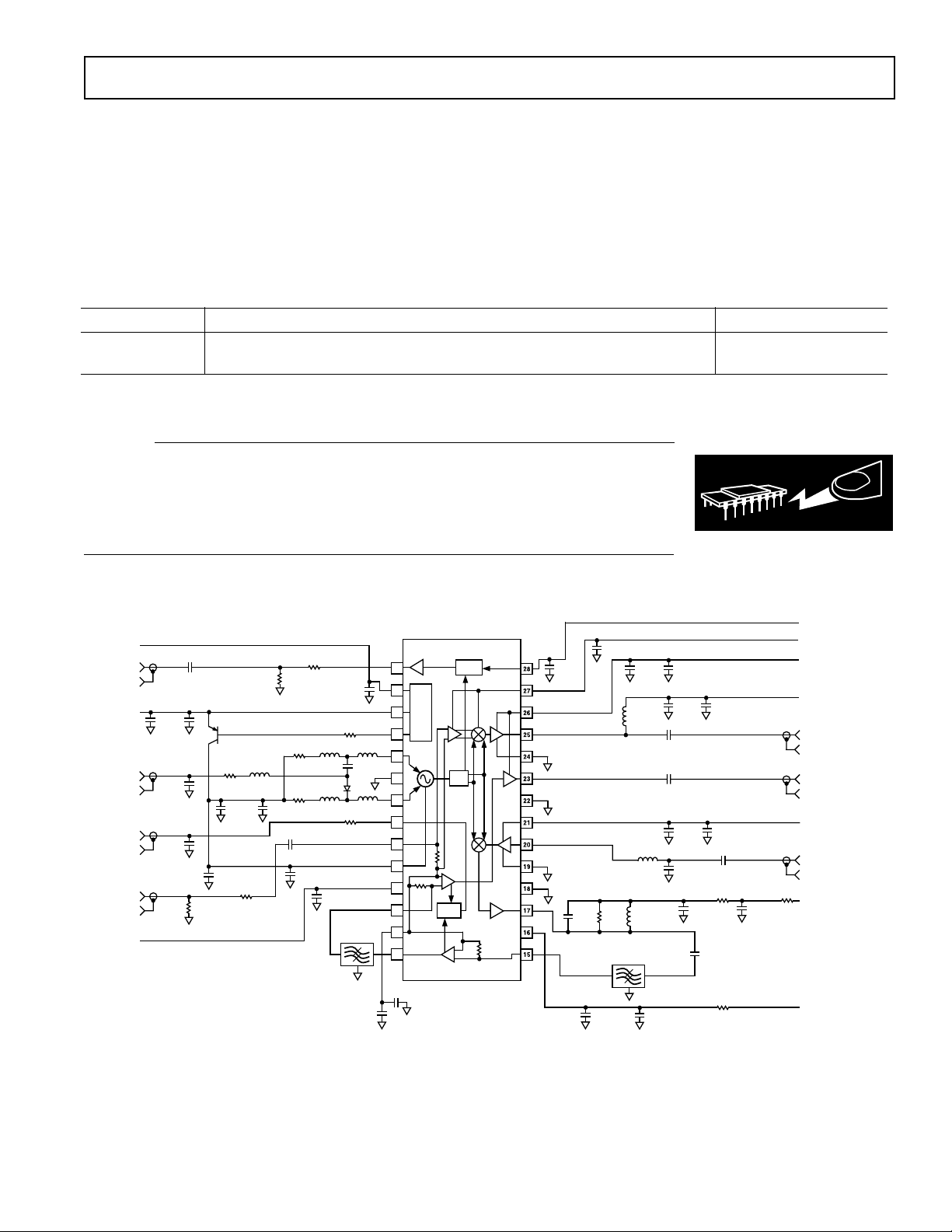
Figure 1. Test Circuit
–3–REV. 0
 Loading...