a
Bandpass ⌺⌬ IF Subsystem
AD6140
FEATURES
IF Subsystem
Bandpass ⌺⌬ Modulator
Variable-Gain Preamplifier with 13 dB of AGC Range
Mixer
AGC Detector
Op Amp for LNA Biasing
ECL-to-CMOS Level Translator
Ultralow Power Design
2.7 V Operating Voltage
4.8 mA Current Consumption
Power-Down Control
Small 20-Lead SSOP Package
APPLICATIONS
FLEX™, ReFLEX™ Receivers
Multimode Receivers
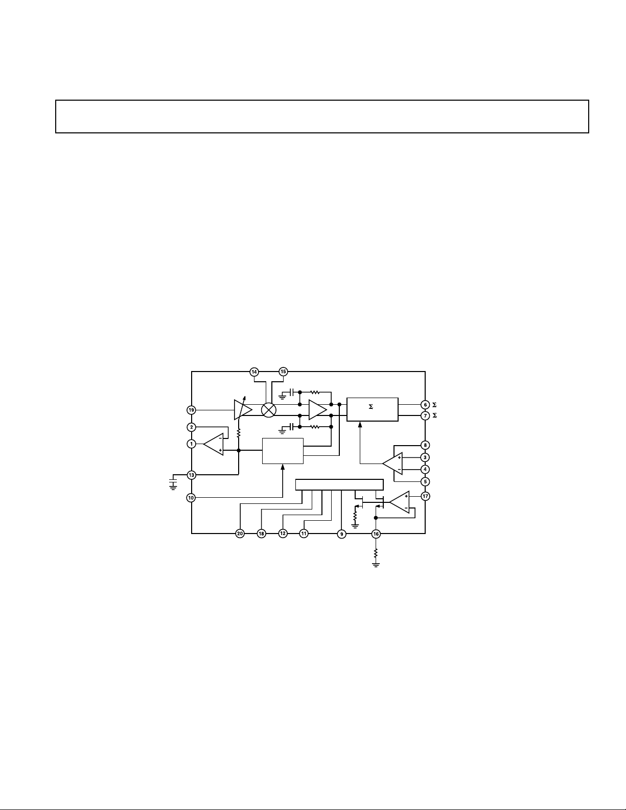
FUNCTIONAL BLOCK DIAGRAM
LO_IN+ LO_IN–
PREAMPLIFIER
IF_INPUT
LNA_SENSE
LNA_FORCE
AGC_CAPACITOR
0.1mF
AGC_TC_SELECT
LNA BIAS
AMPLIFIER
MIXER
AGC
DETECTOR
CIRCUIT
MIXER POST
AMPLIFIER
BIAS SYSTEM
GENERAL DESCRIPTION
The AD6140 is a bandpass Σ∆ ADC IF IC for receivers requiring
a high dynamic range and multiple filter bandwidths. With an
external decimation filter, it creates a multibit analog-to-digital
converter. The AD6140 consists of a variable gain, low noise
preamplifier, mixer, AGC detector, bandpass Σ∆ modulator, an
ECL-to-CMOS level translator for the system clock, and an
auxiliary amplifier for use in biasing a discrete LNA. It is designed to operate with Motorola’s ReFLEX chipset solution.
Contact Motorola directly for more information about the
ReFLEX chipset solution. With data and clock outputs at CMOS
logic levels, it interfaces to an external decimation filter. It comes in
a 20-lead plastic SSOP and operates over the –40°C to +85°C
industrial temperature range at 2.7 V.
AD6140
D
MODULATOR
ECL-TO-CMOS
LEVEL-SHIFTER
D_DATA_OUT
D_CLOCK_OUT
BUFFER_VDD
CLK_IN+
CLK_IN–
BUFFER_GND
VOLTAGE_REFERENCE_IN
AVDD AGND DGND DVDD POWER_DOWN
FLEX and ReFLEX are trademarks of Motorola, Inc.
REV. 0
Information furnished by Analog Devices is believed to be accurate and
reliable. However, no responsibility is assumed by Analog Devices for its
use, nor for any infringements of patents or other rights of third parties
which may result from its use. No license is granted by implication or
otherwise under any patent or patent rights of Analog Devices.
R
INT
BIAS_RESISTOR
39kV
One Technology Way, P.O. Box 9106, Norwood, MA 02062-9106, U.S.A.
Tel: 781/329-4700 World Wide Web Site: http://www.analog.com
Fax: 781/326-8703 © Analog Devices, Inc., 1998

AD6140–SPECIFICATIONS
Specification Conditions Min Typ Max Units
OVERALL VOLTAGE_REFERENCE_IN = 1 V ± 5% dc,
IF = 49.6 MHz
LO = 49.792 MHz or 49.408 MHz, 200 mV p-p
Differential Input
Clock = 6.144 MHz, 800 mV p-p Differential ECL
Input, Clock Asymmetry = 50 ± 2.5%
Input Third Order Intercept Point At Max Gain –27 –19 dBm
Noise Figure At Max Gain, External Termination 10.5 dB
Input Resistance At IF_INPUT (Pin 19) 2.5 kΩ
Input Capacitance At IF_INPUT (Pin 19) 12 pF
Dynamic Range 6.25 kHz Bandwidth Centered at 192 kHz 76 83 dB
Maximum Gain 29.5 dB
Minimum Gain 16 dB
AGC DETECTOR
AGC Threshold –24 dBm
Capacitor Charging Current AGC_TC_SELECT Input = Logic LOW (FAST AGC) 2.8 µA
AGC_TC_SELECT Input = Logic HIGH (SLOW AGC) 50 nA
ECL-TO-CMOS LEVEL VDD (to VDD – 0.8 V) Differential Levels
TRANSLATOR
Clock Output Drive 5 pF Load 2.6 V p-p
Clock Asymmetry 5 pF Load ±2.5 %
LNA BIAS AMPLIFIER VOLTAGE
LNA_FORCE 2.9 V LNA_SENSE, Minimum Gain 1.7 V
LNA_SENSE Input Voltage Range VDD VDD – 0.3 V
POWER-DOWN INTERFACE
Logic Threshold 0.7 V
Turn-On Response Time To Valid Data Output 100 µs
Turn-Off Response Time To Typical Power-Down Supply Current 100 µs
POWER SUPPLY
Supply Voltage 2.5 2.9 V
Supply Current Power-Down Input: Logic LOW = ON, IF_Input = 0 V 4.8 5.75 mA
Power-Down Current Power-Down Input: Logic HIGH = OFF 3 µA
Operating Temperature Range –40 +85 °C
Specifications subject to change without notice.
(TA = +25ⴗC, VCC = 2.7 V, VOLTAGE_REFERENCE_IN = 1 V, unless otherwise noted)
–2–
REV. 0

AD6140
WARNING!
ESD SENSITIVE DEVICE
TOP VIEW
(Not to Scale)
20
19
18
17
16
15
14
13
12
11
1
2
3
4
5
6
7
8
9
10
AD6140
AGC TC SELECT
POWER
DOWN
BUFFER
VDD
LNA
SENSE
CLK
IN+
CLK
IN–
D CLOCK OUT
D DATA OUT
BUFFER
GND
DVDD
DGND
AGC
CAPACITOR
IF
INPUT
AGND
VOLTAGE
REFERENCE IN
LO
IN+
LO
IN–
BIAS
RESISTOR
LNA
FORCE
AVDD
ABSOLUTE MAXIMUM RATINGS
Supply Voltage to Ground . . . . . . . . . . . . . . . . . . . . . . +5.5 V
Internal Power Dissipation
2
. . . . . . . . . . . . . . . . . . . . 50 mW
1
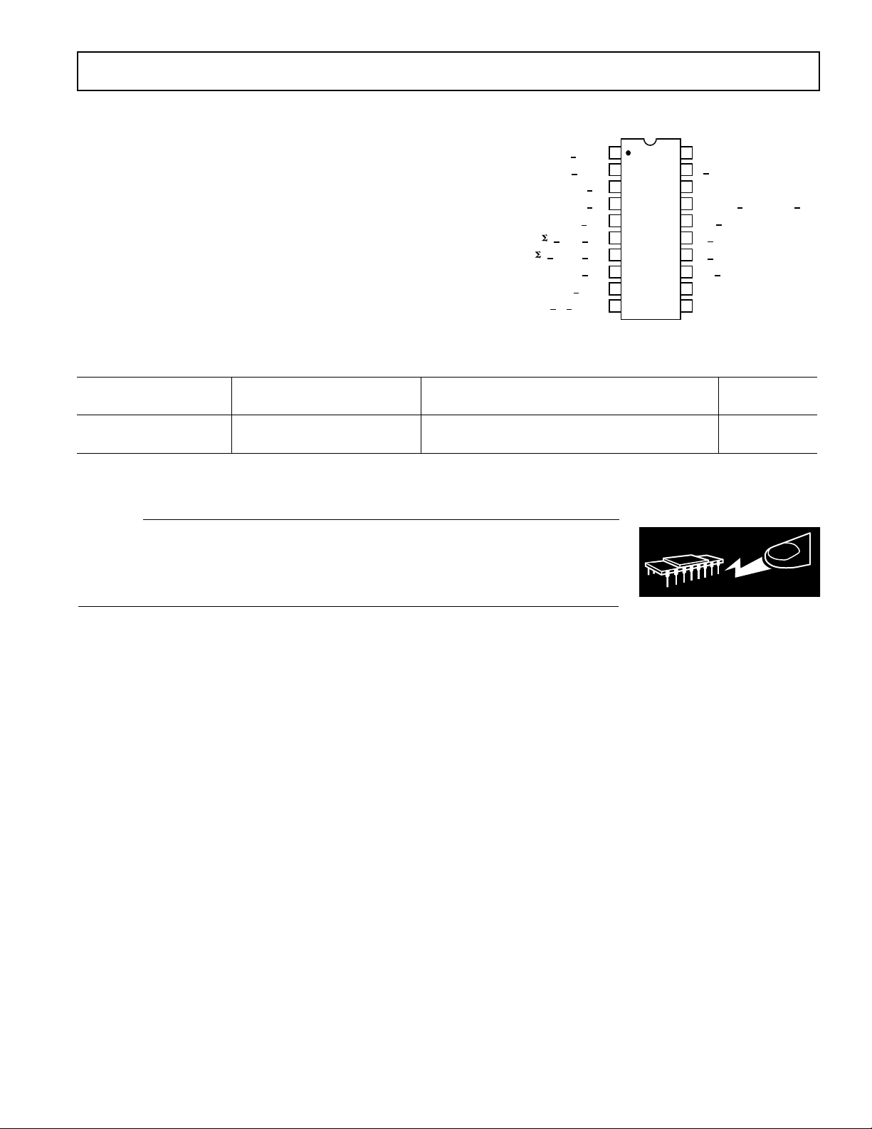
PIN CONFIGURATION
Operating Temperature Range . . . . . . . . . . . –40°C to +85°C
Storage Temperature Range . . . . . . . . . . . . –65°C to +150°C
Lead Temperature, Soldering (60 sec) . . . . . . . . . . . . +300°C
NOTES
1
Stresses above those listed under Absolute Maximum Ratings may cause perma-
nent damage to the device. This is a stress rating only; functional operation of the
device at these or any other conditions above those indicated in the operational
section of this specification is not implied. Exposure to absolute maximum rating
conditions for extended rating conditions for extended periods may affect device
reliability.
2
Thermal Characteristics:
20-Lead SSOP: θJA = 126°C/W.
ORDERING GUIDE
Temperature Package Package
Model Range Description Option
AD6140ARS –40°C to +85°C Shrink Small Outline Package RS-20
AD6140ARSRL –40°C to +85°C 20-Lead Plastic SSOP on Tape-and-Reel
CAUTION
ESD (electrostatic discharge) sensitive device. Electrostatic charges as high as 4000 V readily
accumulate on the human body and test equipment and can discharge without detection.
Although the AD6140 features proprietary ESD protection circuitry, permanent damage may
occur on devices subjected to high energy electrostatic discharges. Therefore, proper ESD
precautions are recommended to avoid performance degradation or loss of functionality.
REV. 0
–3–
 Loading...