CDMA 3 V Transmitter IF Subsystem
a
with Integrated Voltage Regulator
FEATURES
Fully Compliant with IS98A and PCS Specifications
Linear IF Amplifier
–63 dB to +34 dB
Linear-in-dB Gain Control
Temperature-Compensated Gain Control
Quadrature Modulator
Modulates IFs from 50 MHz to 350 MHz
Integral Low Dropout Regulator
Accepts 2.9 V to 4.2 V Input from Battery
Low Power
10.4 mA at Midgain
<10 A Sleep Mode Operation
Companion Receiver IF Chip Available (AD6121)
APPLICATIONS
CDMA, W-CDMA, AMPS and TACS Operation
QPSK Transmitters
GENERAL DESCRIPTION
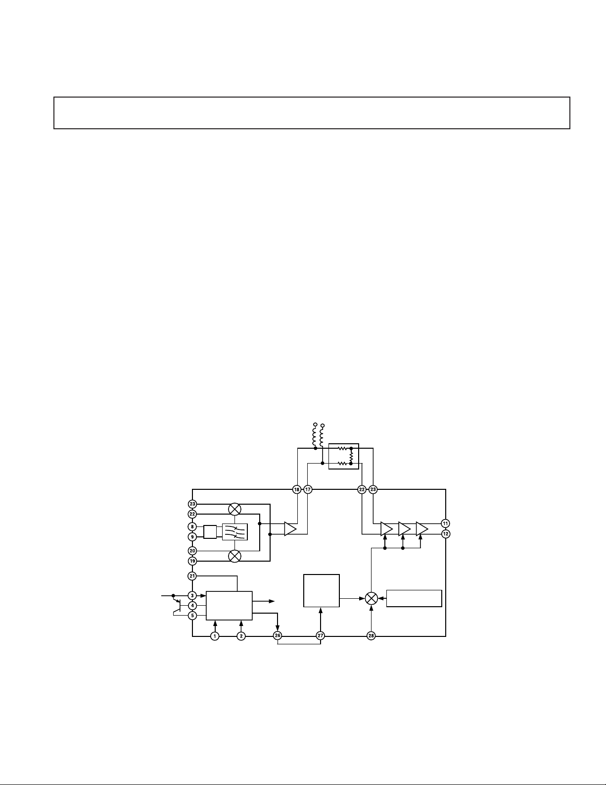
The AD6122 is a low power IF transmitter subsystem, specifically designed for CDMA applications. It consists of an I and Q
modulator, a divide-by-two quadrature generator, high dynamic
AD6122
range IF amplifiers with voltage-controlled gain and a powerdown control input. An integral low dropout regulator allows
operation from battery voltages from 2.9 V to 4.2 V.
The gain control input accepts an external gain control voltage
input from a DAC. It provides 97 dB of gain control with a
nominal 75 dB/V scale factor. Either an internal or an external
reference may be used to set the gain-control scale factor.
The I and Q modulator accepts differential quadrature baseband inputs from a CDMA baseband converter. The local oscillator is injected at twice the IF frequency. A divide-by-two
quadrature generator followed by dual polyphase filters ensures
±1° quadrature accuracy.
The modulator provides a common-mode reference output to
bias the transmit DACs in the baseband converter to the same
common-mode voltage as the modulator inputs, allowing dc
coupling between the two ICs and thus eliminating the need to
charge and discharge coupling capacitors. This allows the fastest
power-up and power-down times for the AD6122 and CDMA
baseband ICs.
The AD6122 is fabricated using a 25 GHz f
process and is packaged in a 28-lead SSOP and a 32-leadless
LPCC chip scale package (5 mm × 5 mm).
silicon BiCMOS
t
I INPUT
LOCAL
OSCILLATOR
INPUT
Q INPUT
COMMON-MODE
REFERENCE
OUTPUT
VPOS
FUNCTIONAL BLOCK DIAGRAM
QUADRATURE
MODULATOR
OUTPUT
QUADRATURE MODULATOR
ⴜ2
POWERDOWN 2
VREG
1.23 V
REFERENCE
OUTPUT
LOW
DROPOUT
REGULATOR
POWERDOWN 1
VCC
ATTENUATOR
AD6122
GAIN
CONTROL
SCALE
FACTOR
GAIN CONTROL
REFERENCE
VOLTAGE
INPUT
IF AMPLIFIER
INPUT
IF AMPLIFIERS
GAIN CONTROL
VOLTAGE
INPUT
TEMPERATURE
COMPENSATION
TRANSMIT
OUTPUT
REV. B
Information furnished by Analog Devices is believed to be accurate and
reliable. However, no responsibility is assumed by Analog Devices for its
use, nor for any infringements of patents or other rights of third parties
which may result from its use. No license is granted by implication or
otherwise under any patent or patent rights of Analog Devices.
One Technology Way, P.O. Box 9106, Norwood, MA 02062-9106, U.S.A.
Tel: 781/329-4700 World Wide Web Site: http://www.analog.com
Fax: 781/326-8703 © Analog Devices, Inc., 2000

AD6122–SPECIFICATIONS
(TA = +25ⴗC, VCC = +3.0 V, LO = 2 ⴛ IF, REFIN = 1.23 V, LDO Enabled, unless otherwise
noted) NOTE: All powers shown in dBm are referred to 1 k⍀.
Specification Conditions Min Typ Max Unit
MODULATOR LO = 260.76 MHz (2 × IF), 100 mV p-p
500 mV p-p Differential I and Q Inputs;
Output Level Output Level Referred to a 1 kΩ Differential Load –21 dBm
Output Third Order Harmonic –50 dBc
I/Q Inputs
Differential Input Voltage Differential 500 mV p-p
Bandwidth –3 dB 20 MHz
Resistance 30 kΩ
Quadrature Accuracy ±1 °
Amplitude Balance ±0.1 dB
Output Referred Noise 0.9 MHz to 5.0 MHz Offsets –169 dBm/Hz
Modulator Common-Mode Reference 1.408 V
LO Input Resistance Differential Input at 260.38 MHz 1.2 kΩ
LO Input Capacitance Differential Input at 260.38 MHz 2.4 pF
LO Carrier Leakage Bias I/Q Using MODCMREF –40 dBc
IF AMPLIFIER F
Noise Figure VGAIN = 2.5 V, 1 kΩ Differential Load 10 dB
Input 1 dB Compression Point VGAIN = 2.5 V –32 dBm
Input Third-Order Intercept VGAIN = 2.5 V –24 dBm
Gain Flatness IF ±630 kHz ±0.25 dB
Input Capacitance Shunt Equivalent Model at 130.38 MHz 2.3 pF
Differential IF Input Resistance Shunt Equivalent Model at 130.38 MHz 680 Ω
Differential IF Output Resistance Per Pin at 130.38 MHz 4.2 kΩ
Differential IF Output Capacitance Per Pin at 130.38 MHz 2.0 pF
GAIN CONTROL INTERFACE
Gain Scaling Using Internal Reference 75 dB/V
Gain Scaling Linearity For a Typical Dynamic Range of 92 dB ±3 dB/V
Minimum Gain VGAIN = 0.5 V –63 dB
Maximum Gain VGAIN = 2.5 V +34 dB
Gain Control Response Time 90 dB Gain Change, Min Gain to Max Gain 0.7 µs
Input Resistance at REFIN 10 MΩ
Input Resistance at VGAIN 109 kΩ
POWER-DOWN INTERFACE
Logic Threshold High Power-Up on Logical High 1.34 V
Logic Threshold Low 1.30 V
Input Current for Logical High 0.1 µA
Turn-On Response Time Measure to Settling of AGC from Standby Mode 23 µs
Turn-Off Response Time To 200 µA Supply Current 187 ns
LOW DROPOUT REGULATOR External PNP Pass Transistor, VCE
Input Range 2.9–4.2 V
Nominal Output 2.70 V
Dropout Voltage 200 mV
Reference Output 1.23 V
POWER SUPPLY
Supply Range Bypassing Internal LDO 2.7–5.0 V
Supply Current VGAIN = 1.5 V (Unity Gain) 10.4 mA
Standby Current 7.8 µA
OPERATING TEMPERATURE
T
to T
MIN
Specifications subject to change without notice.
MAX
= 130.38 MHz
IF
Max, h
= 100/300 Min/Max
FE
= –0.4 V
SAT
–40 +85 °C
–2–
REV. B

AD6122
WARNING!
ESD SENSITIVE DEVICE
ABSOLUTE MAXIMUM RATINGS
1
Supply Voltage DVCC, IFVCC, TXVCC to DGND,
IFGND . . . . . . . . . . . . . . . . . . . . . . . . . . . . . . . . . . . . +5 V
Internal Power Dissipation
2
. . . . . . . . . . . . . . . . . . . 600 mW
Operating Temperature Range . . . . . . . . . . . –40°C to +85°C
Storage Temperature Range . . . . . . . . . . . . –65°C to +150°C
Lead Temperature Range (Soldering 60 sec) . . . . . . . . +300°C
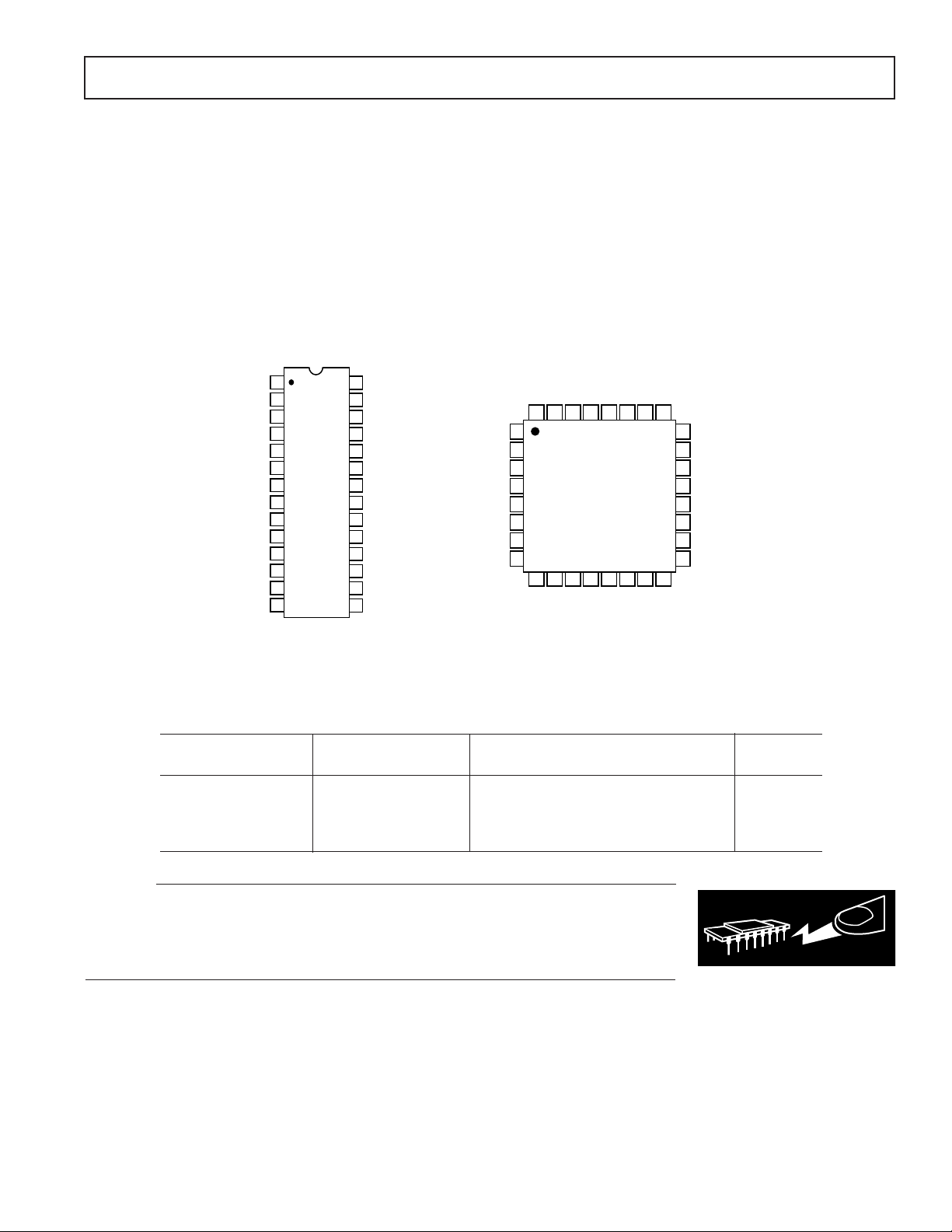
PIN CONFIGURATIONS
SSOP Package
PD1
PD2
LDOE
LDOB
LDOC
LDOGND
DGND
LOIPP
LOIPN
DVCC
TXOPP
TXOPN
TXVCC
IFGND
1
2
3
4
5
6
AD6122
7
TOP VIEW
(Not to Scale)
8
9
10
11
12
13
14
28
VGAIN
27
REFIN
26
REFOUT
25
IFVCC
24
IFGND
IIPP
23
22
IIPN
21
MODCMREF
QIPN
20
19
QIPP
18
MODOPP
17
MODOPN
16
IFINP
15
IFINN
NOTES
1
Stresses above those listed under Absolute Maximum Ratings may cause perma-
nent damage to the device. This is a stress rating only; functional operation of the
device at these or any other conditions above those indicated in the operational
section of this specification is not implied. Exposure to absolute maximum rating
conditions for extended periods may affect device reliability.
2
Thermal Characteristics: 28-lead SSOP Package: θJA = 115.25°C/W.
LPCC Package
REFIN
LDOB
LDOC
LDOGND
LDOGND
DGND
LOIPP
LOIPN
DVCC
VGAIN
PD1
PD2
LDOE
32
1
223
3
421
AD6122 Top View
5
619
7
8
(Not to Scale)
10311130122913281427152616
9
IFGND
IFGND
TXVCC
TXOPP
TXOPN
NC
IFVCC
REFOUT
25
24
IFGND
IFGND
22
IIPP
IIPN
20
MODCMREF
QIPN
QIPP
18
17
MODOPP
IFINP
IFINN
MODOPN
NC = NO CONNECT
ORDERING GUIDE
Temperature Package
Model Range Package Description Option
AD6122ARS –40°C to +85°C Shrink Small Outline Package (SSOP) RS-28
AD6122ARSRL –40°C to +85°C 28-Lead SSOP on Tape-and-Reel
AD6122ACP –40°C to +85°C Chip Scale Package (LPCC) CP-32
AD6122ACPRL –40°C to +85°C 32-Leadless LPCC on Tape-and-Reel
CAUTION
ESD (electrostatic discharge) sensitive device. Electrostatic charges as high as 4000 V readily
accumulate on the human body and test equipment and can discharge without detection.
Although the AD6122 features proprietary ESD protection circuitry, permanent damage may
occur on devices subjected to high-energy electrostatic discharges. Therefore, proper ESD
precautions are recommended to avoid performance degradation or loss of functionality.
REV. B
–3–

AD6122
PIN FUNCTION DESCRIPTIONS
SSOP LPCC
Pin # Pin # Pin Label Description Function
1 30 PD1 Power-Down 1 IF Amplifier Power-Down Control Input; CMOS Com-
patible; HIGH = Entire IC Powers Down, LOW = IF
Amplifiers On.
2 31 PD2 Power-Down 2 Modulator Power-Down Control Input; CMOS Compat-
ible; HIGH = Modulator Off , LOW = Modulator On.
3 32 LDOE Low Dropout Regulator Pass Connects to Emitter of External PNP Pass Transistor
Transistor Emitter Connection and VCC.
4 1 LDOB Low Dropout Regulator Pass Connects to Base of External PNP Pass Transistor.
Transistor Base
5 2 LDOC Low Dropout Regulator Pass Connects to Collector of External PNP Pass Transistor.
Transistor Collector
6 3, 4 LDOGND Low Dropout Regulator Ground Ground.
7 5 DGND Digital Ground Ground.
8 6 LOIPP Local Oscillator “Positive” Input Connects to Local Oscillator; AC Coupled.
9 7 LOIPN Local Oscillator “Negative” Input Connects to Ground via Decoupling Capacitor.
10 8 DVCC Digital VCC Connects to Digital Supply.
11 9 TXOPP Transmit Output “Positive” Connects to Output Filter; AC Coupled.
12 10 TXOPN Transmit Output “Negative” Connects to Output Filter; AC Coupled.
13 11 TXVCC Transmit Output VCC Connects to LDO Output via Decoupling Network.
14 12, 13 IFGND IF Ground Ground.
15 14 IFINN IF Input “Negative” IF “Negative” Input from LC Roofing Filter.
16 15 IFINP IF Input “Positive” IF “Positive” Input from LC Roofing Filter.
17 16 MODOPN Modulator “Negative” If Output Output Modulator Output to LC Roofing Filter.
18 17 MODOPP Modulator “Positive” Output Modulator Output to LC Roofing Filter.
19 18 QIPP Q Input “Positive” Connects to Q “Positive” Output of Baseband IC.
20 19 QIPN Q Input “Negative” Connects to Q “Negative” Output of Baseband IC.
21 20 MODCMREF Modulator Common-Mode Connects to CDMA Baseband Converter Tx DAC
Reference Out Common-Mode Reference Input.
22 21 IIPN I Input “Negative” Connects to I “Negative” Output of Baseband IC.
23 22 IIPP I Input “Positive” Connects to I “Positive” Output of Baseband IC.
24 23, 24 IFGND Ground Connects to IF Ground.
25 NC No Connect
25 26 IFVCC IF VCC Connects to Decoupled Output of LDO Regulator.
26 27 REFOUT Gain Control Reference Output Provides 1.23 V Voltage Reference Output for DAC in
CDMA Baseband Converter and REFIN.
27 28 REFIN Gain Control Reference Input Accepts 1.23 V Reference Input from REFOUT or
External Reference.
28 29 VGAIN Gain Control Voltage Input Accepts Gain Control Input Voltage from External DAC.
Max Gain = 2.5 V; Min Gain = 0.5 V.
–4–
REV. B

Test Figures
MUST BE EQUAL
LENGTHS
I DATA
MUST BE EQUAL
LENGTHS
Q DATA
50⍀
50⍀
MODCMREF
MODCMREF
MODCMREF
MODCMREF
AD6122
0.1F
+15V
8
V
X1
X2
Y1
Y2
–15V
+15V
X1
X2
Y1
Y2
–15V
+15V
X1
X2
Y1
Y2
–15V
+15V
X1
X2
Y1
Y2
–15V
V–1
V–1
V–1
V–1
V–1
V–1
V–1
V–1
P
V
N
5
8
V
P
V
N
5
8
V
P
V
N
5
8
V
P
V
N
5
OUT
A=1
AD830
0.1F
0.1F
OUT
A=1
AD830
0.1F
0.1F
OUT
A=1
AD830
0.1F
0.1F
OUT
A=1
AD830
0.1F
7
50⍀
IIPP
AD6122
7
7
7
50⍀
50⍀
50⍀
IIPN
QIPP
QIPN
LOIPP
MODOPP
MODOPN
LOIPN
VREG OUT
10nF
10nF
VREG OUT
MODCMREF
0.1F
450⍀
205⍀
450⍀
0.1F
MOD_OUT
1
2
3
4
1
2
3
4
1
2
3
4
1
2
3
4
REV. B
LO INPUT
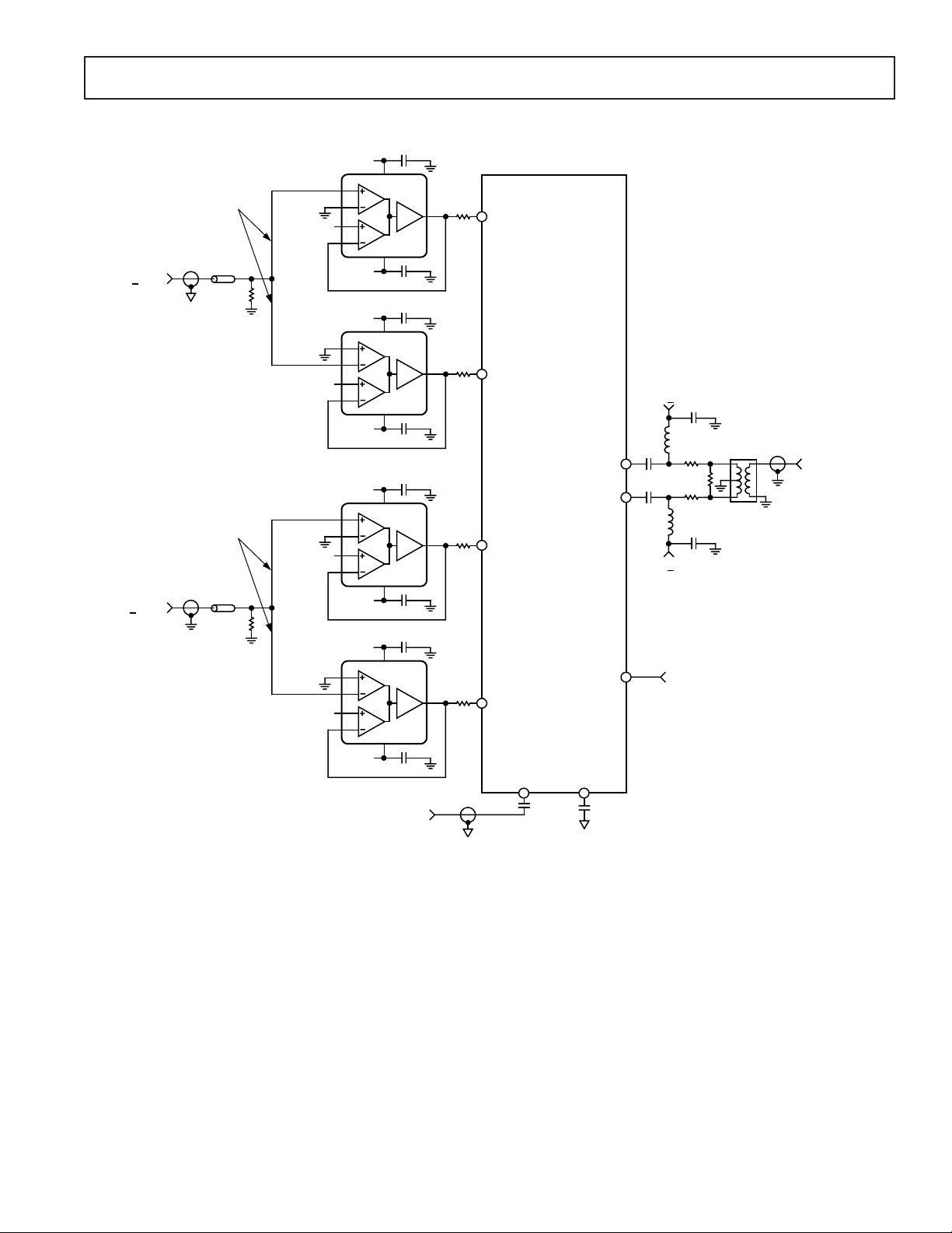
Figure 1. Quadrature Modulator’s Characterization Input and Output Impedance Matches
–5–

AD6122
VREG OUT
10nF
10nF
0.1F
453⍀
205⍀
453⍀
4:1
RF SOURCE
1:8
PULL-UP INDUCTORS CHOSEN
FOR PEAK RESPONSE AT THE
TEST FREQUENCY.
383⍀
511⍀
383⍀
IFINP TXOPP
10nF
IFINN
10nF
TXOPN
AD6122
0.1F
VREG OUT
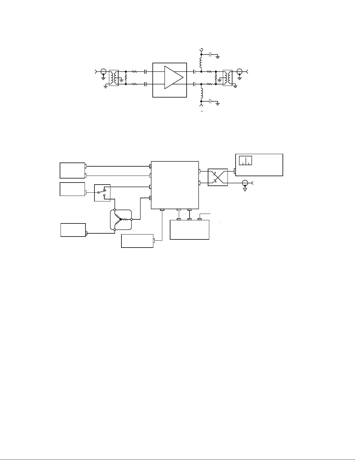
Figure 2. IF Amplifier’s Characterization Input and Output Impedance Matches
NOTE: RF CABLES FOR I AND Q PATHS MUST BE OF EQUAL LENGTH
TEST BED MOTHERBOARD
I CHANNEL
Q CHANNEL
LO INPUT
IF IN
MOD OUT
IFTX OUT
TO RF SWITCHES
TEKTRONIX
AFG2002
R&S
SMT03
RF
RF SOURCE 1
I DATA
500mVp-p DIFFERENTIAL
Q DATA
RF
INPUT
TO
SPECTRUM
ANALYZER
R&S FSEA20/30
SPECTRUM
ANALYZER
AUX MEAS
PORT
R&S
SMT03
RF SOURCE 2
RF
HPE3610
POWER SUPPLY
Figure 3. General Test Set
HP34970A
DATA ACQUISITION
& SWITCH CONTROL
DC MEASUREMENTS
& CONTROL BITS
–6–
REV. B
 Loading...