REV. B
Information furnished by Analog Devices is believed to be accurate and
reliable. However, no responsibility is assumed by Analog Devices for its
use, nor for any infringements of patents or other rights of third parties
which may result from its use. No license is granted by implication or
otherwise under any patent or patent rights of Analog Devices.
a
AD6121
One Technology Way, P.O. Box 9106, Norwood, MA 02062-9106, U.S.A.
Tel: 781/329-4700 World Wide Web Site: http://www.analog.com
Fax: 781/326-8703 © Analog Devices, Inc., 2000
CDMA 3 V Receiver IF Subsystem
with Integrated Voltage Regulator
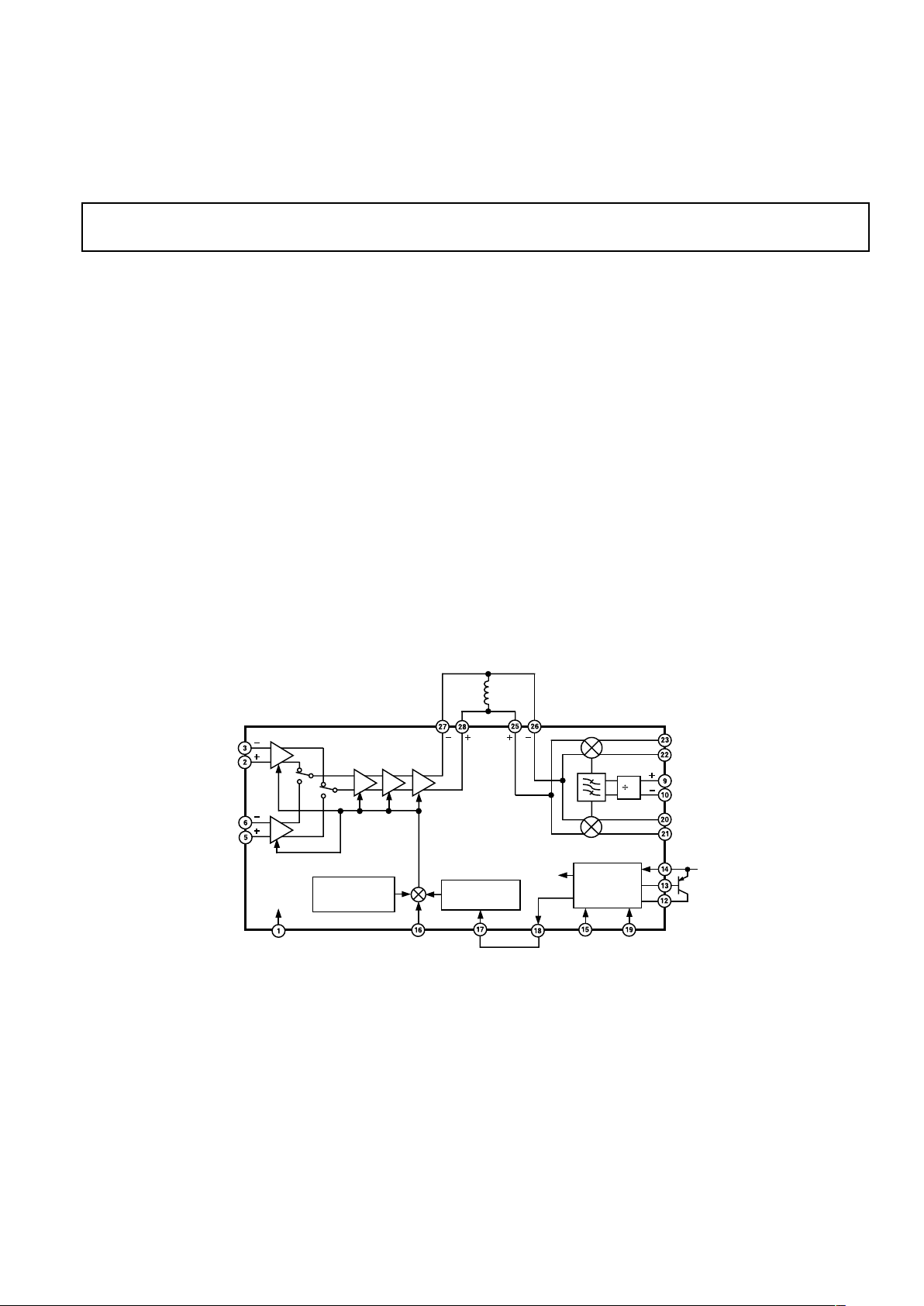
FUNCTIONAL BLOCK DIAGRAM
2
I
Q
ROOFING
FILTER
IF
OUTPUT
DEMODULATOR
INPUT
IF AMPLIFIERS
INPUT STAGE
QUADRATURE DEMODULATOR
CDMA
INPUT
FM
INPUT
CDMA/FM
SELECT
GAIN
CONTROL
VOLTAGE
INPUT
1.23V
REFERENCE
OUTPUT
GAIN
CONTROL
VOLTAGE
REFERENCE
INPUT
POWERDOWN 2
POWERDOWN 1
IOUT
IOUT
QOUT
QOUT
LOCAL
OSCILLATOR
INPUT
VPOS
VREG
LOW
DROPOUT
REGULATOR
GAIN CONTROL
SCALE FACTOR
PTAT
TEMPERATURE
COMPENSATION
AD6121
FEATURES
Fully Compliant with IS98A and PCS Specifications
CDMA, W-CDMA, AMPS, and TACS Operation
Linear IF Amplifier
5.9 dB Noise Figure
–47.5 dB to +47 dB Linear-in-dB Gain Control
Quadrature Demodulator
Demodulates IFs from 50 MHz to 350 MHz
Integral Low Dropout Regulator
200 mV Voltage Drop
Accepts 2.9 V to 4.2 V Input from Battery
Low Power
10 mA at Midgain
<1 A Sleep Mode Operation
Companion Transmitter IF Chip Available (AD6122)
APPLICATIONS
CDMA, W-CDMA, AMPS, and TACS Operation
QPSK Receivers
GENERAL DESCRIPTION
The AD6121 is a low power receiver IF subsystem specifically
designed for CDMA applications. It consists of high dynamic
range IF amplifiers with voltage controlled gain, a divide-by-two
quadrature generator, an I and Q demodulator, and a powerdown control input. An integral low dropout regulator allows
operation from battery voltages from 2.9 V to 4.2 V.
The gain control input accepts an external gain control voltage
input from a DAC. It provides 94.5 dB of gain control with a
nominal 52.5 dB/V scale factor when using an internal voltage
reference. The gain control interface reference input can be
connected to either the internal reference or an external reference.
The I and Q demodulator provides differential quadrature baseband outputs to interface with CDMA baseband converters. A
divide-by-two quadrature generator followed by dual polyphase
filters ensures maximum ±2.5° quadrature accuracy.
The AD6121 IF Subsystem is fabricated using a 25 GHz f
t
BiCMOS silicon process and is packaged in a 28-lead SSOP
and a 32-leadless LPCC chip scale package (5 mm × 5 mm).

–2–
REV. B
AD6121–SPECIFICATIONS
(TA = +25ⴗC, VCC = 3.0 V, LO = 2 ⴛ IF, REFIN = 1.23 V, LDO Enabled, unless otherwise
noted) Note: All power measurements in dBm are referred to 1 k⍀ unless ZIN is noted.
Specification Conditions Min Typ Max Units
TOTAL GAIN
Maximum Gain IF Amplifiers and Demodulator Powered Up +47 dB
IF Amplifiers Powered Up and Demodulator Powered Down +41.4 dB
Minimum Gain IF Amplifier and Demodulator Powered Up –47.5 dB
IF AMPLIFIER
CDMA and FM Input IF = 85.38 MHz
Noise Figure Maximum Gain 5.9 dB
Input Third-Order Intercept Maximum Gain –42.8 dBm
Input 1 dB Compression Point Maximum Gain –51.6 dBm
Gain Flatness IF ± 630 kHz, CDMA Mode ± 0.25 dB
CDMA Input Capacitance Differential 2.8 pF
CDMA Input Resistance Differential 850 Ω
FM Input Capacitance Differential 2.3 pF
FM Input Resistance Differential 670 Ω
Output Capacitance Differential 1.35 pF
Output Resistance Differential 1.1 kΩ
GAIN CONTROL INTERFACE
Gain Scaling Using Internal Reference 52.5 dB/V
Gain Scaling Accuracy Within a Gain Control Range of 90 dB ± 3 dB/V
Gain Control Response Time Minimum Gain to Maximum Gain 695 ns
Input Resistance at REFIN 10 MΩ
Input Resistance at VGAIN 100 kΩ
DEMODULATOR LO = 172.76 MHz , –15 dBm Referred to 50 Ω,
Baseband Frequency = 1 MHz
Differential Input Impedance 1kΩ
Differential Input Capacitance at
Demodulator Input 2.9 pF
Input Third Order Intercept –6.1 dBm
Demodulation Gain 5.6 dB
I/Q Output
Differential Output Voltage 10 kΩ, 2 pF Differential Parallel Load Impedance 700 mV p-p
Bandwidth –3 dB 16 MHz
Resistance Single-Ended 630 Ω
Quadrature Accuracy ± 2.5 Degree
Amplitude Balance ± 0.1 ± 0.35 dB
LO Input Impedance Differential 1.5 kΩ
LO Input Capacitance Differential 4.16 pF
CONTROL INTERFACES
Logic Threshold High 1.34 V
Logic Threshold Low 1.30 V
Input Current for Logic High 0.1 µA
Mode Control Response Time CDMA/FM Pin High Selects CDMA, Low Selects FM 430 ns
Turn-On Response Time PD1 and PD2 Pins Low Select IC ON, High Selects IC OFF 2.8 µs
Turn-Off Response Time To 200 µA Supply Current 6.8 µs
LOW DROPOUT REGULATOR External PNP Pass Transistor, VCE
SAT
= –0.4 V Max
h
FE
= 100/300 Min/Max
Input Range 2.9 4.2 V
Nominal Output 2.70 V
Voltage Drop 200 mV
Reference Output 1.23 V
POWER SUPPLY
Supply Range Using Internal LDO Supply Input at Pin LDOE 2.9–5.0 V
Supply Range Bypassing Internal LDO Supply Input at Pins DVCC, IFVCC, LDOC 2.7–3.6 V
Supply Current VGAIN = 1.5 V 10 mA
Standby Current 0.78 µA
OPERATING TEMPERATURE
T
MIN
to T
MAX
–40 +85 °C
Specifications subject to change without notice.

AD6121
–3–
REV. B
ABSOLUTE MAXIMUM RATINGS
1
Supply Voltage VPS1, VPS2 to COM1, COM2 . . . . . . . +5 V
Internal Power Dissipation
2
. . . . . . . . . . . . . . . . . . . 600 mW
Operating Temperature Range . . . . . . . . . . . –40°C to +85°C
Storage Temperature Range . . . . . . . . . . . . –65°C to +150°C
Lead Temperature Range (Soldering 60 sec) . . . . . . . . +300°C
ORDERING GUIDE
Temperature Package Package
Model Range Description Option
AD6121ARS –40°C to +85°C Shrink Small Outline Package (SSOP) RS-28
AD6121ARSRL –40°C to +85°C 28-Lead SSOP on Tape and Reel
AD6121ACP –40°C to +85°C Chip Scale Package (LPCC) CP-32
AD6121ACPRL –40°C to +85°C 32-Leadless LPCC on Tape and Reel
CAUTION
ESD (electrostatic discharge) sensitive device. Electrostatic charges as high as 4000 V readily
accumulate on the human body and test equipment and can discharge without detection.
Although the AD6121 features proprietary ESD protection circuitry, permanent damage may
occur on devices subjected to high-energy electrostatic discharges. Therefore, proper ESD
precautions are recommended to avoid performance degradation or loss of functionality.
WARNING!
ESD SENSITIVE DEVICE
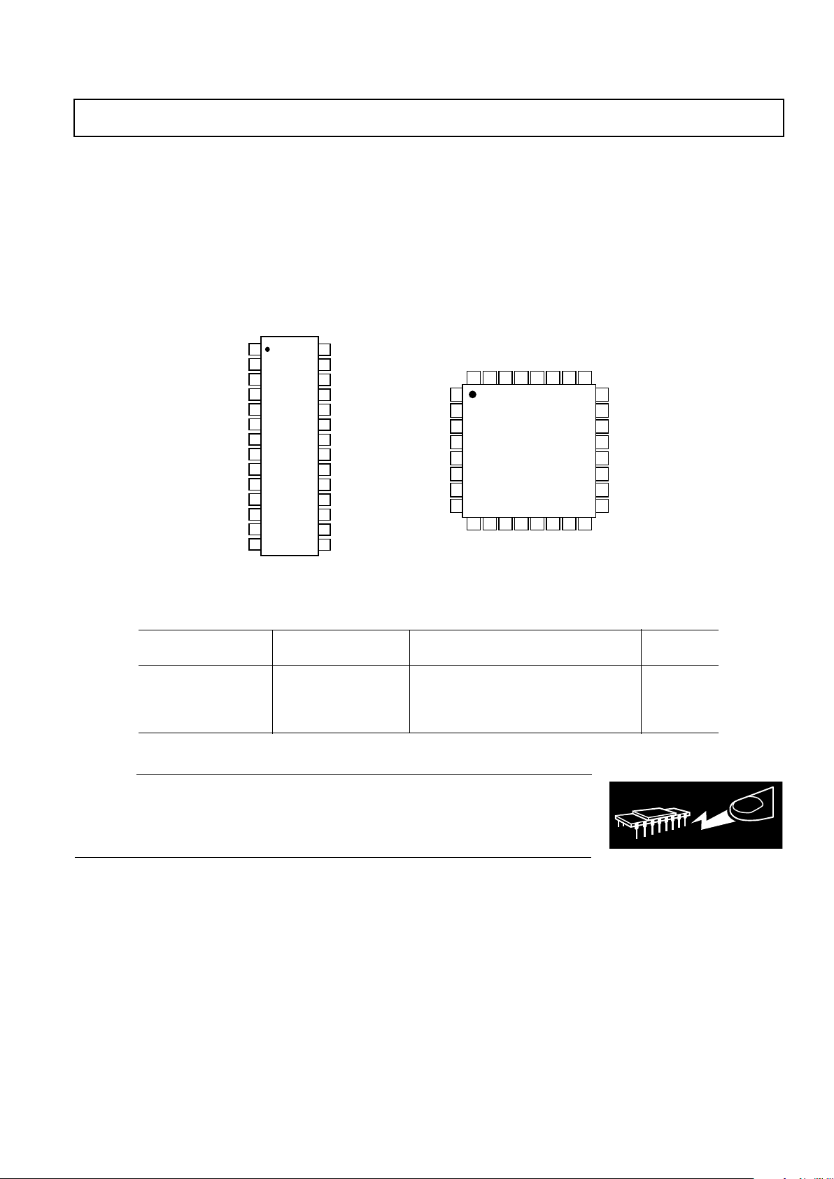
PIN CONFIGURATION
2
23
IFGND
LDOGND
3
22
FMIPP
IOPP
4
21
FMIPN
IOPN
5
20
IFVCC
QOPP
6
19DGND
QOPN
7
18
LOIPP
PD1
8
17LOIPN
REFOUT
1
24
IFGND
LDOGND
10311130122913281427152616
25
DVCC
CDMAIPP
LDOC
CDMA/FM
LDOB
IFOPP
LDOE
IFOPN
PD2
DEMIPN
VGAIN
DEMIPP
REFIN
NC
9
32
NC
CDMAIPN
AD6121 Top View
(Not to Scale)
TOP VIEW
(Not to Scale)
28
27
26
25
24
23
22
21
20
19
18
17
16
15
1
2
3
4
5
6
7
8
9
10
11
12
13
14
AD6121
LDOE
LDOB
LDOC
DVCC
LOIPN
LOIPP
DGND
CDMA/FM
CDMAIPP
CDMAIPN
IFGND
IFVCC
FMIPN
FMIPP
PD2
VGAIN
REFIN
REFOUT
PD1
QOPN
QOPP
IFOPP
IFOPN
DEMIPN
DEMIPP
IOPN
IOPP
LDOGND
SSOP Package LPCC Package
NC = NO CONNECT
NOTES
1
Stresses above those listed under Absolute Maximum Ratings may cause perma-
nent damage to the device. This is a stress rating only; functional operation of the
device at these or any other conditions above those indicated in the operational
section of this specification is not implied. Exposure to absolute maximum rating
conditions for extended periods may affect device reliability.
2
Thermal Characteristics: 28-lead SSOP Package: θJA = 115.25°C/W.

AD6121
–4–
REV. B
PIN FUNCTION DESCRIPTIONS
SSOP LPCC
Pin Pin
Number Number Pin Label Description Function
1 30 CDMA/FM Selects CDMA or FM Input CMOS-compatible; HIGH = CDMA, LOW = FM.
2 31 CDMAIPP CDMA “Positive” Input AC-coupled, IF input from CDMA SAW filter.
3 32 CDMAIPN CDMA “Negative” Input AC-coupled, IF input from CDMA SAW filter.
4 1, 2 IFGND IF Ground Ground.
5 3 FMIPP FM “Positive” Input AC-coupled, IF input from FM SAW filter.
6 4 FMIPN FM “Negative” Input AC-coupled, IF input from FM SAW filter.
7 5 IFVCC IF VCC VCC for IF AGC amplifiers.
8 6 DGND Digital Ground Ground.
9 7 LOIPP Local Oscillator “Positive” Input AC-coupled, Differential Local Oscillator Input.
10 8 LOIPN Local Oscillator “Negative” Input AC-coupled, Differential Local Oscillator Input.
9, 25 NC No Connect
11 10 DVCC Digital VCC VCC for control logic.
12 11 LDOC Low Dropout Regulator Pass Connects to collector of external PNP pass transistor.
Transistor Collector Connection
13 12 LDOB Low Dropout Regulator Pass Connects to base of external PNP pass transistor.
Transistor Base Connection
14 13 LDOE Low Dropout Regulator Pass Connects to emitter of external PNP pass transistor
Transistor Emitter Connection and DVCC, IFVCC.
15 14 PD2 Demodulator Power-Down Demodulator Power-Down Control Input CMOS-
Control Input compatible; HIGH = Modulator Off, LOW = Modulator On.
16 15 VGAIN Gain Control Voltage Input Accepts gain control input voltage from external DAC.
Max Gain = 2.5 V. Min Gain = 0.5 V.
17 16 REFIN Gain Control Reference Input Accepts 1.23 V reference input from REFOUT (Pin 17)
or external reference.
18 17 REFOUT Reference Output Provides 1.23 V reference output to REFIN (Pin 18) and
CDMA baseband IC reference input so that gain control
DAC and AD6121 use same reference.
19 18 PD1 IF Amplifier Power-Down IF Amplifier Power-Down Control Input, CMOS com-
Control Input patible; HIGH = Entire IC Powers Down, LOW = IF
Amplifier On.
20 19 QOPN Q Output “Negative” Connects to Q “Negative” Input of baseband IC.
21 20 QOPP Q Output “Positive” Connects to Q “Positive” Input of baseband IC.
22 21 IOPN I Output “Negative” Connects to I “Negative” Input of baseband IC.
23 22 IOPP I Output “Positive” Connects to I “Positive” Input of baseband IC.
24 23, 24 LDOGND Ground Ground.
25 26 DEMIPP Demodulator “Positive” IF Input Demodulator input from roofing filter.
26 27 DEMIPN Demodulator “Negative” IF Input Demodulator input from roofing filter.
27 28 IFOPN IF Amplifier “Negative” IF Output IF output to roofing filter.
28 29 IFOPP IF Amplifier “Positive” IF Output IF output to roofing filter.

AD6121
–5–
REV. B
Test Figures
RF
SOURCE
1:8
909⍀
110⍀
110⍀
10nF
1k⍀
453⍀
205⍀
4:1
TO
SPECTRUM
ANALYZER
CDMAIPP
CDMAIPN
IFOPP
INDUCTOR CHOSEN FOR PEAK RESPONSE
AT THE TEST FREQUENCY (SEE TEXT)
IFOPN
AD6121
10nF
10nF
10nF
453⍀
a. CDMA Input Port Characterization Impedance Match
50⍀
10nF
IFOPP
IFOPN
AD6121
FMIPP
FMIPN
10nF
453⍀
RF
SOURCE
b. FM Input Port Characterization Impedance Match
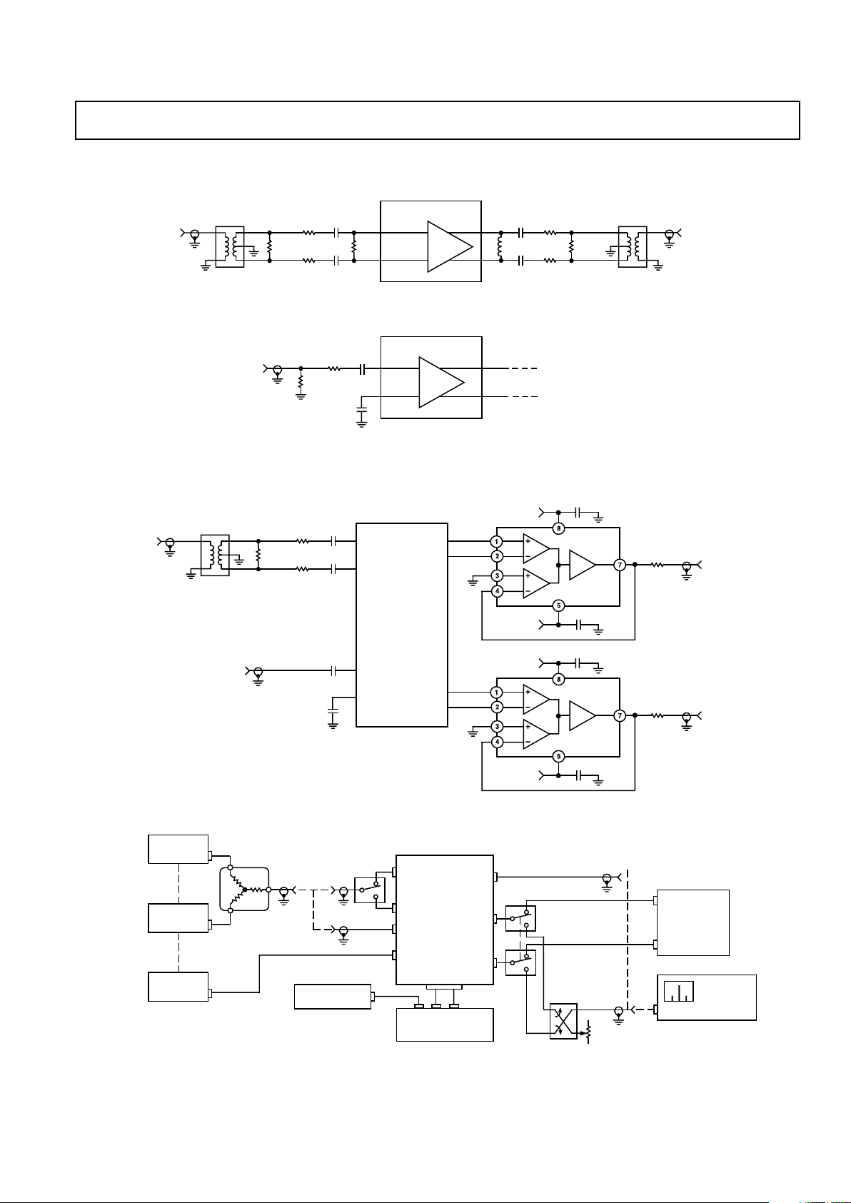
Figure 1. Quadrature Modulator Characterization Input and Output Impedance Matches
I CHANNEL
AD830
+15V
0.1F
–15V
OUT
Y2
Y1
X2
X1
A=1
50⍀
V–1
V–1
V
P
V
N
0.1F
10nF
205⍀
453⍀
453⍀
Q CHANNEL
LO
SOURCE
10nF
RF
SOURCE
10nF
10nF
1:4
ALL SIGNAL PATHS MUST BE EQUAL
LENGTHS FOR I/Q MEASUREMENTS
AD830
+15V
0.1F
–15V
OUT
Y2
Y1
X2
X1
A=1
50⍀
V–1
V
P
V
N
0.1F
V–1
DEMIPP
DEMIPN
IOPP
IOPN
AD6121
QUADRATURE
DEMODULATOR
LOIPP
LOIPN
QOPP
QOPN
Figure 2. IF Amplifier Characterization Input and Output Impedance Matches
R&S FSEA
SPECTRUM
ANALYZER
RF INPUT
R & S
SMT03
RF
HP34970A
DATA ACQUISITION
& SWITCH CONTROL
ALL DC MEASUREMENT
AND CONTROL SIGNALS
SYNC
REFERENCE
SYNC
REFERENCE
50⍀
TERMINATOR
HP8508A
VECTOR
VOLTMETER
CH1
CH2
R & S
SMT03
RF
R & S
SMT03
RF
IF OUT
CDMA
IN
FM IN
DEMOD
IN
LO
INPUT
I CHANNEL
Q CHANNEL
DC I/O
AD6121
HPE3610
POWER SUPPLY
Figure 3. General Test Set
 Loading...