Low Power Mixer/Limiter/RSSI
a
FEATURES
Mixer
–15 dBm 1 dB Compression Point
–5 dBm IP3
24 dB Conversion Gain
>500 MHz Input Bandwidth
Logarithmic/Limiting Amplifier
80 dB RSSI Range
638 Phase Stability over 80 dB Range
Low Power
21 mW at 3 V Power Consumption
CMOS-Compatible Power-Down to 300 mW typ
200 ns Enable/Disable Time
APPLICATIONS
PHS, GSM, TDMA, FM, or PM Receivers
Battery-Powered Instrumentation
Base Station RSSI Measurement
GENERAL DESCRIPTION
The AD608 provides both a low power, low distortion, low
noise mixer and a complete, monolithic logarithmic/limiting
amplifier using a “successive-detection” technique. It provides
both a high speed RSSI (Received Signal Strength Indicator)
output with 80 dB dynamic range and a hard-limited output.
The RSSI output is from a two-pole post-demodulation lowpass filter and provides a loadable output voltage of +0.2 V to
+1.8 V. The AD608 operates from a single 2.7 V to 5.5 V supply at a typical power level of 21 mW at 3 V.
3 V Receiver IF Subsystem
AD608
The RF and LO bandwidths both exceed 500 MHz. In a typical
IF application, the AD608 will accept the output of a 240 MHz
SAW filter and downconvert it to a nominal 10.7 MHz IF with
a conversion gain of 24 dB (Z
rithmic/limiting amplifier section handles any IF from LF to as
high as 30 MHz.
The mixer is a doubly-balanced “Gilbert-Cell” type and operates linearly for RF inputs spanning –95 dBm to –15 dBm. It
has a nominal –5 dBm third-order intercept. An onboard LO
preamplifier requires only –16 dBm of LO drive. The mixer’s
current output drives a reverse-terminated, industry-standard
10.7 MHz 330 Ω filter.
The nominal logarithmic scaling is such that the output is
+0.2 V for a sinusoidal input to the IF amplifier of –75 dBm
and +1.8 V at an input of +5 dBm; over this range the logarithmic conformance is typically ±1 dB. The logarithmic slope is
proportional to the supply voltage. A feedback loop automatically nulls the input offset of the first stage down to the submicrovolt level.
The AD608’s limiter output provides a hard-limited signal output at 400 mV p-p. The voltage gain of the limiting amplifier to
this output is more than 100 dB. Transition times are 11 ns and
the phase is stable to within ± 3° at 10.7 MHz for signals from
–75 dBm to +5 dBm.
The AD608 is enabled by a CMOS logic-level voltage input,
with a response time of 200 ns. When disabled, the standby
power is reduced to 300 µW within 400 ns.
The AD608 is specified for the industrial temperature range of
–25°C to +85°C for 2.7 V to 5.5 V supplies and –40°C to +85°C
for 4.5 V to 5.5 V supplies. It comes in a 16-pin plastic SOIC.
= 165 Ω). The AD608’s loga-
IF
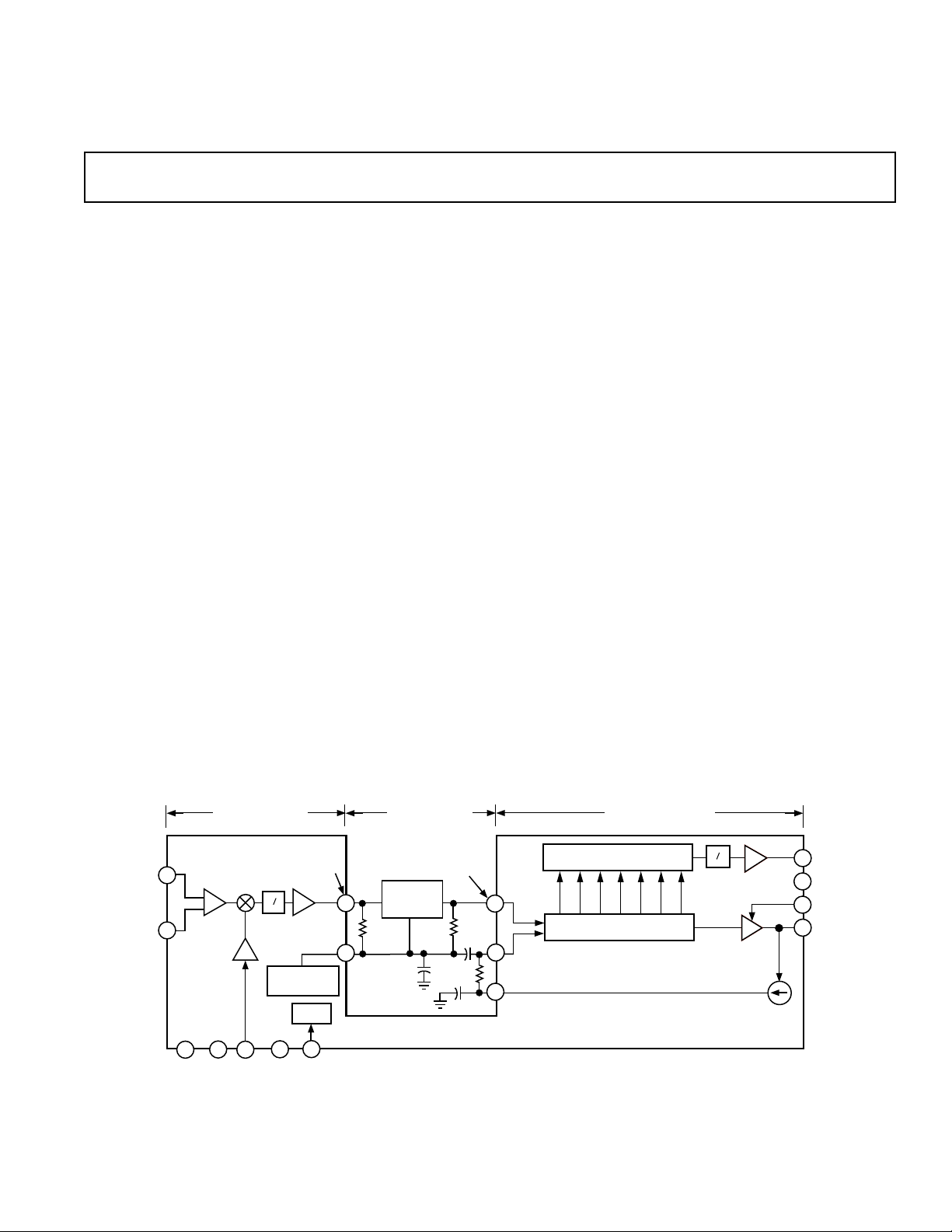
FUNCTIONAL BLOCK DIAGRAM
RFHI
RF INPUT
–95 TO
–15dBm
RFLO
5
1
6
VPS1 COM1
+2.7V TO
5.5V
PREAMP
1
24dB MIXER GAIN
±6mA MAX OUTPUT
(±890mV INTO 165Ω)
MIXER
≈
LO
MID-SUPPLY
LOHI
COM2
2 4
3
LO INPUT
–16dBm
MXOP
BPF
DRIVER
VMID
IF BIAS
BIAS
PRUP
16
CMOS LOGIC
INPUT
7
8
3dB NOMINAL
INSERTION LOSS
10.7MHz
BANDPASS
FILTER
330Ω
100nF
IF INPUT
–75dBm TO
+15dBm
330Ω
100Ω
18nF
10nF
REV. B
Information furnished by Analog Devices is believed to be accurate and
reliable. However, no responsibility is assumed by Analog Devices for its
use, nor for any infringements of patents or other rights of third parties
which may result from its use. No license is granted by implication or
otherwise under any patent or patent rights of Analog Devices.
110dB LIMITER GAIN
90dB RSSI
RSSI OUTPUT
7 FULL-WAVE
2
IFHI
9
10
IFLO
13
FDBK
RECTIFIER CELLS
5-STAGE IF AMPLIFIER
(16dB PER STAGE)
≈
2MHz
LPF
AD608
NOTES:
One Technology Way, P.O. Box 9106, Norwood, MA 02062-9106, U.S.A.
Tel: 617/329-4700 Fax: 617/326-8703
1
–15dBm = ±56mV MAX FOR LINEAR OPERATION
2
39.76µV RMS TO 397.6mV RMS FOR ±1dB RSSI
ACCURACY
RSSI
20mV/dB
11
COM3
VPS2
LMOP
FINAL
LIMITER
±50µA
© Analog Devices, Inc., 1996
0.2V TO 1.8V
12
+2.7V TO 5.5V
14
15
LIMITER
OUTPUT
400mVp-p

AD608–SPECIFICA TIONS
(@ TA = + 258C, Supply = 3 V, dBm is referred to 50 V, unless otherwise noted)
Model AD608
Conditions Min Typ Max Units
MIXER PERFORMANCE
RF and LO Frequency Range 500 MHz
LO Power Input Terminated in 50 Ω –16 dBm
Conversion Gain Driving Doubly-Terminated 330 Ω IF Filter, Z
Noise Figure Matched Input, f
Matched Input, f
= 100 MHz 11 dB
RF
= 240 MHz 16 dB
RF
= 165 Ω 19 24 28 dB
IF
1 dB Compression Point Input Terminated in 50 Ω –15 dBm
Third-Order Intercept f
Input Resistance f
= 240 MHz and 240.02 MHz, fLO = 229.3 MHz –5 dBm
RF
= 100 MHz (See Table I) 1.9 kΩ
RF
Input Capacitance fRF = 100 MHz (See Table I) 3 pF
LIMITER PERFORMANCE
Gain Full Temperature and Supply Range 110 dB
Limiting Threshold 3° rms Phase Jitter at 10.7 MHz –75 dBm
280 kHz IF Bandwidth
Input Resistance 10 kΩ
Input Capacitance 3pF
Phase Variation –75 dBm to +5 dBm IF Input Signal at 10.7 MHz ±3 Degree
DC Level Center of Output Swing (VPOS-1) 2 V
Output Level Limiter Output Driving 5 kΩ Load 400 mV p-p
Rise and Fall Times Driving a 5 pF Load 11 ns
Output Impedance 200 Ω
RSSI PERFORMANCE At 10.7 MHz
Nominal Slope At VPOS = 3 V; Proportional to VPOS 17.27 20 23.27 mV/dB
Nominal Intercept –85 dBm
Minimum RSSI Voltage –75 dBm Input Signal 0.2 V
Maximum RSSI Voltage +5 dBm Input Signal 1.8 V
RSSI Voltage Intercept 0 dBm Input Signal 1.57 1.82 V
Logarithmic Linearity Error –75 dBm to +5 dBm Input Signal at IFHI ±1dB
RSSI Response Time 90% RF to 50% RSSI 200 ns
Output Impedance At Midscale 250 Ω
POWER-DOWN INTERFACE
Logical Threshold System Active on Logical High 1.5 V
Input Current For Logical High 75 µA
Power-Up Response Time Active Limiter Output 200 ns
Power-Down Response Time To 200 µA Supply Current 400 ns
Power-Down Current 100 µA
POWER SUPPLY
Operating Range –25°C to +85°C 2.7 5.5 V
–40°C to +85°C 4.5 5.5 V
Powered Up Current VPOS = 3 V 7.3 mA
OPERATING TEMPERATURE
T
to T
MIN
T
MIN
Specifications subject to change without notice.
to T
MAX
MAX
VPOS = 2.7 V to 5.5 V –25 +85 °C
VPOS = 4.5 V to 5.5 V –40 +85 °C
–2–
REV. B

AD608
WARNING!
ESD SENSITIVE DEVICE
VPS1
COM1
PRUP
LMOP
RFHI
RFLO
MXOP
COM3
RSSI
IFLO
LOHI
COM2
VPS2
FDBK
VMID IFHI
1
2
16
15
5
6
7
12
11
10
3
4
14
13
89
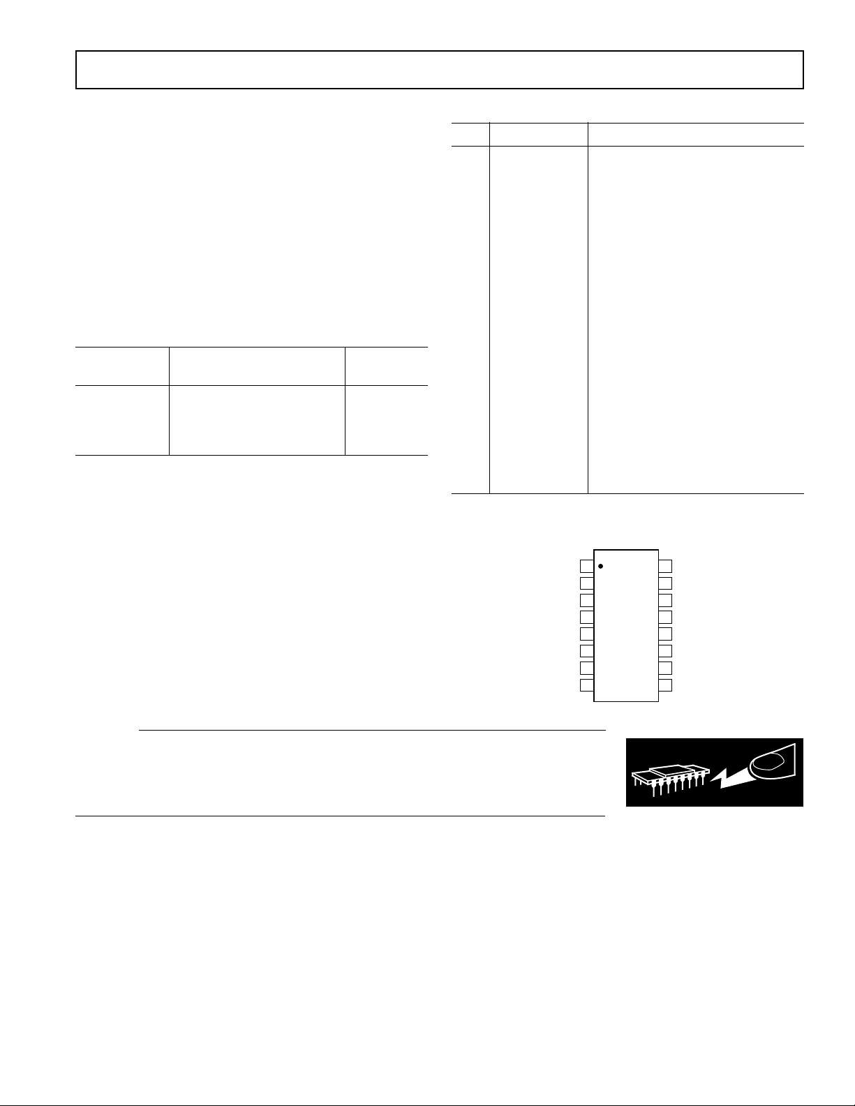
TOP VIEW
(Not to Scale)
AD608
ABSOLUTE MAXIMUM RATINGS
Supply Voltage VPS1, VPS2 . . . . . . . . . . . . . . . . . . . . . . +6 V
Internal Power Dissipation
2
. . . . . . . . . . . . . . . . . . . .600 mW
1
Temperature Range . . . . . . . . . . . . . . . . . . . . .–40°C to +85°C
Storage Temperature Range . . . . . . . . . . . . .–65°C to +150°C
Lead Temperature (Soldering 60 sec) . . . . . . . . . . . . . +300°C
NOTES
1
Stresses above those listed under “Absolute Maximum Ratings” may cause
permanent damage to the device. This is a stress rating only, and functional
operation of the device at these or any other conditions above those indicated in the
operational section of this specification is not implied. Exposure to absolute
maximum rating conditions for extended rating conditions for extended periods
may affect device reliability.
2
Thermal Characteristics:
16-Pin SOIC Package: θJA = 110°C/W.
ORDERING GUIDE
Temperature Package
Model Range Option
AD608AR –25°C to +85°C, R-16A*
2.7 V to 5.5 V Supplies;
–40°C to +85°C,
4.5 V to 5.5 V Supplies
*R = Small Outline IC (SOIC).
PIN DESCRIPTIONS
Pin Mnemonic Description
1 VPS1 Positive Supply Input
2 COM1 Common
3 LOHI Local Oscillator Input Connection
4 COM2 Common
5 RFHI RF Input, Noninverting
6 RFLO RF Input, Inverting
7 MXOP Mixer Output
8 VMID Midpoint Supply Bias
Output
9 IFHI IF Input, Noninverting
10 IFLO IF Input, Inverting
11 RSSI Received Signal Strength Indicator
Output
12 COM3 Output Common
13 FDBK Offset-Null Feedback Loop Output
14 VPS2 Limiter Positive Supply Input
15 LMOP Limiter Output
16 PRUP Power-Up
TERMINAL DIAGRAM
CAUTION
ESD (electrostatic discharge) sensitive device. Electrostatic charges as high as 4000 V readily
accumulate on the human body and test equipment and can discharge without detection.
Although the AD608 features proprietary ESD protection circuitry, permanent damage may
occur on devices subjected to high energy electrostatic discharges. Therefore, proper ESD
precautions are recommended to avoid performance degradation or loss of functionality.
REV. B
–3–

AD608
INPUT POWER AT IFHI – dBm
RSSI – V
3.0
0
–80 –70 10
–60 –50 –40 –20 –10 0–30
2.5
2.0
1.5
1.0
0.5
5V
3V
1
2
3
4
5
6
7
8
16
15
14
13
12
11
10
9
AD608
VPS1
COM1
RFHI
RFLO
MXOP
LOHI
COM2
VMID
PRUP
LMOP
COM3
RSSI
IFLO
VPS2
FDBK
IFHI
VPOS
LO IN
RF IN
IF OUT
NC
NC
0.1µF
1nF
51.1Ω
1nF
332Ω
301Ω
0.1µF
54.9Ω
51.1Ω
1nF
0.1µF
332Ω
10nF
100Ω
18nF
18nF
47kΩ
NC = NO CONNECT
PRUP IN
4.7k
1
0.1µF
332Ω
2
3
4
5
6
7
8
VPS1
COM1
LOHI
COM2
RFHI
RFLO
MXOP
VMID
VPOS
51.1Ω
0.1µF
51.1Ω
1nF
1nF
AD608
0.1µF
332Ω
U1 – 74HC00
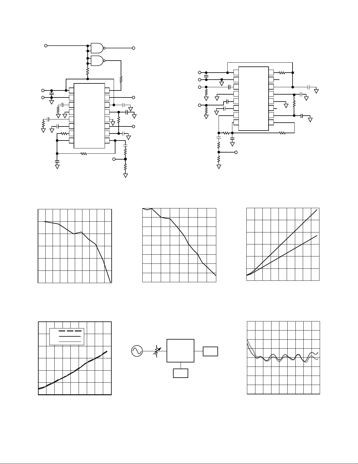
Figure 1. IF Test Board Schematic
25.0
24.5
24.0
23.5
23.0
CONVERSION GAIN – dB
22.5
22.0
100 150 200 250 300 350 400 450
0 50 500
RF FREQUENCY – MHz
U1A
U1B
PRUP
LMOP
VPS2
FDBK
COM3
RSSI
IFLO
IFHI
16
15
14
13
12
11
10
9
IF INPUT
47kΩ
0.1µF
18nF
100Ω
10nF
301Ω
54.9Ω
TRIGGER
LMOP OUT
RSSI OUTPUT
0.1µF
0
–1
–2
–3
–4
–5
RESPONSE – dB
–6
–7
–8
010 80
20 30 40 50 60 70
IF FREQUENCY – MHz
Figure 2. Mixer Test Board Schematic
Figure 3. Mixer Conversion Gain vs.
Frequency
3.0
2.5
2.0
1.5
RSSI – V
1.0
0.5
Figure 6. IF RSSI Output vs.
Temperature (3 V Supply)
+85
+25
–25
0
–60 –50 –40 –20 –10 0–30
INPUT POWER – dBm
–80 –70 10
Figure 4. Mixer IF Port Bandwidth
FLUKE 6082A
SYNTHESIZER
10.7 MHz
Figure 7. Test Circuit for IF RSSI Output vs. Supply Voltage (Ambient Temperature) (Figure 5) and IF RSSI
Output vs. Temperature (3 V Supply)
IF TEST BOARD
IFHI
RSSI
VPOS
DCPS 3V
HP3366A
(Figure 6) and RSSI Error vs. Input
Power (Figure 8)
–4–
DMM
HP34401A
Figure 5. IF RSSI Output vs. Supply
Voltage (Ambient Temperature)
4.0
3.0
2.0
1.0
0
–1.0
RSSI ERROR – dB
–2.0
–3.0
–4.0
–80 –70 10–60 –50 –40 –20 –10 0–30
INPUT POWER – dBm
3V
5V
Figure 8. RSSI Error vs. Input Power
REV. B
 Loading...