Low Power Mixer
a
FEATURES
Complete Receiver-on-a-Chip: Monoceiver® Mixer
–15 dBm 1 dB Compression Point
–8 dBm Input Third Order Intercept
500 MHz RF and LO Bandwidths
Linear IF Amplifier
Linear-in-dB Gain Control
Manual Gain Control
Quadrature Demodulator
On-Board Phase-Locked Quadrature Oscillator
Demodulates IFs from 400 kHz to 12 MHz
Can Also Demodulate AM, CW, SSB
Low Power
25 mW at 3 V
CMOS Compatible Power-Down
Interfaces to AD7013 and AD7015 Baseband Converters
APPLICATIONS
GSM, CDMA, TDMA, and TETRA Receivers
Satellite Terminals
Battery-Powered Communications Receivers
3 V Receiver IF Subsystem
AD607
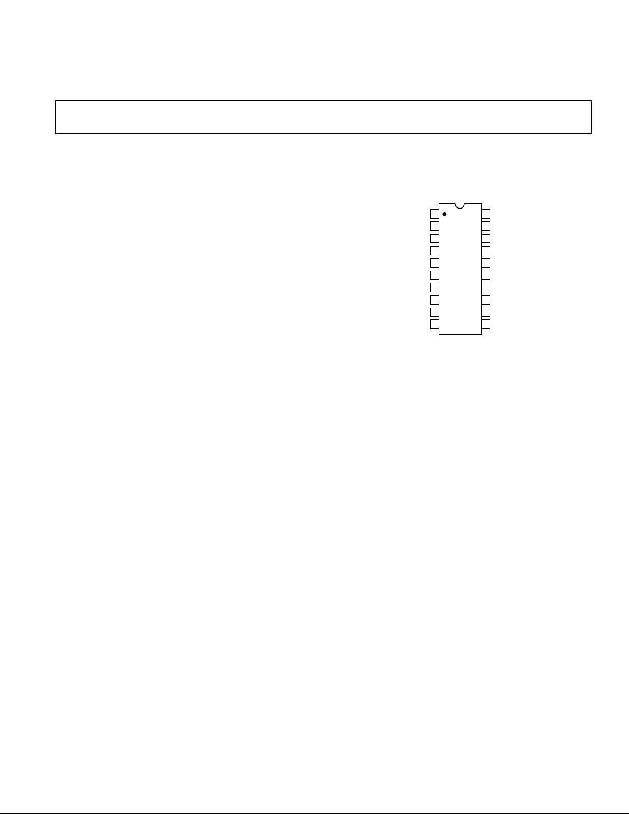
PIN CONFIGURATION
20-Lead SSOP
(RS Suffix)
FDIN
COM1
PRUP
LOIP
RFLO
RFHI
GREF
MXOP
VMID
IFHI
1
2
3
4
5
AD607
TOP VIEW
6
(Not to Scale)
7
8
9
10
20
VPS1
19
FLTR
18
IOUT
17
QOUT
16
VPS2
15
DMIP
14
IFOP
13
COM2
12
GAIN
11
IFLO
GENERAL DESCRIPTION
The AD607 is a 3 V low power receiver IF subsystem for operation at input frequencies as high as 500 MHz and IFs from
400 kHz to 12 MHz. It consists of a mixer, IF amplifiers, I and
Q demodulators, a phase-locked quadrature oscillator, and a
biasing system with external power-down.
The AD607’s low noise, high intercept mixer is a doubly
balanced Gilbert cell type. It has a nominal –15 dBm input
referred 1 dB compression point and a –8 dBm input referred
third order intercept. The mixer section of the AD607 also
includes a local oscillator (LO) preamplifier, which lowers the
required LO drive to –16 dBm.
In MGC operation, the AD607 accepts an external gain-control
voltage input from an external AGC detector or a DAC.
Monoceiver is a registered trademark of Analog Devices, Inc.
The I and Q demodulators provide in-phase and quadrature
baseband outputs to interface with Analog Devices’ AD7013
(IS54, TETRA, MSAT) and AD7015 (GSM) baseband converters. A quadrature VCO phase-locked to the IF drives the I
and Q demodulators. The I and Q demodulators can also
demodulate AM; when the AD607’s quadrature VCO is phaselocked to the received signal, the in-phase demodulator becomes
a synchronous product detector for AM. The VCO can also be
phase-locked to an external beat-frequency oscillator (BFO),
and the demodulator serves as a product detector for CW or
SSB reception. Finally, the AD607 can be used to demodulate
BPSK using an external Costas Loop for carrier recovery.
REV. C
Information furnished by Analog Devices is believed to be accurate and
reliable. However, no responsibility is assumed by Analog Devices for its
use, nor for any infringements of patents or other rights of third parties that
may result from its use. No license is granted by implication or otherwise
under any patent or patent rights of Analog Devices.
One Technology Way, P.O. Box 9106, Norwood, MA 02062-9106, U.S.A.
Tel: 781/329-4700 www.analog.com
Fax: 781/326-8703 © Analog Devices, Inc., 2002

AD607–SPECIFICATIONS
(@ TA = 25ⴗC, Supply = 3.0 V, IF = 10.7 MHz, unless otherwise noted.)
AD607ARS
Model Conditions Min Typ Max Unit
DYNAMIC PERFORMANCE
MIXER
Maximum RF and LO Frequency Range For Conversion Gain > 20 dB 500 MHz
Maximum Mixer Input Voltage For Linear Operation; Between RFHI and RFLO ± 54 mV
Input 1 dB Compression Point RF Input Terminated in 50 Ω –15 dBm
Input Third-Order Intercept RF Input Terminated in 50 Ω –5 dBm
Noise Figure Matched Input, Max Gain, f = 83 MHz, IF = 10.7 MHz 14 dB
Matched Input, Max Gain, f = 144 MHz, IF = 10.7 MHz 12 dB
Maximum Output Voltage at MXOP Z
Mixer Output Bandwidth at MXOP –3 dB, Z
= 165 Ω, at Input Compression ± 1.3 V
IF
= 165 Ω 45 MHz
IF
LO Drive Level Mixer LO Input Terminated in 50 Ω –16 dBm
LO Input Impedance LOIP to VMID 1 kΩ
Isolation, RF to IF RF = 240 MHz, IF = 10.7 MHz, LO = 229.3 MHz 30 dB
Isolation, LO to IF RF = 240 MHz, IF = 10.7 MHz, LO = 229.3 MHz 20 dB
Isolation, LO to RF RF = 240 MHz, IF = 10.7 MHz, LO = 229.3 MHz 40 dB
Isolation, IF to RF RF = 240 MHz, IF = 10.7 MHz, LO = 229.3 MHz 70 dB
IF AMPLIFIERS
Noise Figure Max Gain, f = 10.7 MHz 17 dB
Input 1 dB Compression Point IF = 10.7 MHz –15 dBm
Output Third-Order Intercept IF = 10.7 MHz 18 dBm
Maximum IF Output Voltage at IFOP Z
= 600 Ω±560 mV
IF
Output Resistance at IFOP From IFOP to VMID 15 Ω
Bandwidth –3 dB at IFOP, Max Gain 45 MHz
GAIN CONTROL (See Figures 23 and 24)
Gain Control Range Mixer + IF Section, GREF to 1.5 V 90 dB
Gain Scaling GREF to 1.5 V 20 mV/dB
GREF to General Reference Voltage V
R
75/V
R
dB/V
Gain Scaling Accuracy GREF to 1.5 V, 80 dB Span ± 1dB
Bias Current at GAIN 5 µA
Bias Current at GREF 1 µA
Input Resistance at GAIN, GREF 1MΩ
I AND Q DEMODULATORS
Required DC Bias at DMIP VPOS/2 V dc
Input Resistance at DMIP From DMIP to VMID 50 kΩ
Input Bias Current at DMIP 2 µA
Maximum Input Voltage IF > 3 MHz ±150 mV
IF ≤ 3 MHz ±75 mV
Amplitude Balance IF = 10.7 MHz, Outputs at 600 mV p-p, F = 100 kHz ± 0.2 dB
Quadrature Error IF = 10.7 MHz, Outputs at 600 mV p-p, F = 100 kHz –1.2 Degrees
Phase Noise in Degrees IF = 10.7 MHz, F = 10 kHz –100 dBc/Hz
Demodulation Gain Sine Wave Input, Baseband Output 18 dB
Maximum Output Voltage R
Output Offset Voltage Measured from I
≥ 20 kΩ±1.23 V
L
OUT
, Q
to VMID –150 +10 +150 mV
OUT
Output Bandwidth Sine Wave Input, Baseband Output 1.5 MHz
PLL
Required DC Bias at FDIN VPOS/2 V dc
Input Resistance at FDIN From FDIN to VMID 50 kΩ
Input Bias Current at FDIN 200 nA
Frequency Range 0.4 to 12 MHz
Required Input Drive Level Sine Wave Input at Pin 1 400 mV
Acquisition Time to ± 3° IF = 10.7 MHz 16.5 µs
POWER-DOWN INTERFACE
Logical Threshold For Power Up on Logical High 2 V dc
Input Current for Logical High 75 µA
Turn-On Response Time To PLL Locked 16.5 µs
Standby Current 550 µA
POWER SUPPLY
Supply Range 2.92 5.5 V
Supply Current Midgain, IF = 10.7 MHz 8.5 mA
OPERATING TEMPERATURE
to T
T
MIN
MAX
Operation to 2.92 V Minimum Supply Voltage –25 +85 °C
Operation to 4.5 V Minimum Supply Voltage –40 +85 °C
Specifications subject to change without notice.
–2–
REV. C

AD607
ABSOLUTE MAXIMUM RATINGS
Supply Voltage VPS1, VPS2 to COM1, COM2 . . . . . . . 5.5 V
Internal Power Dissipation
2
. . . . . . . . . . . . . . . . . . . . 600 mW
1
2.92 V to 5.5 V Operating Temperature Range
. . . . . . . . . . . . . . . . . . . . . . . . . . . . . . . . . . –25°Cto+85°C
4.5 V to 5.5 V Operating Temperature Range
. . . . . . . . . . . . . . . . . . . . . . . . . . . . . . . . . . –40°C to +85°C
Storage Temperature Range . . . . . . . . . . . . –65°C to +150°C
Lead Temperature Range (Soldering 60 sec) . . . . . . . . . 300°C
NOTES
1
Stresses above those listed under Absolute Maximum Rating may cause permanent damage to the device. This is a stress rating only; functional operation of the
device at these or any other conditions above those indicated in the operational
section of this specification is not implied. Exposure to absolute maximum rating
conditions for extended periods may affect device reliability.
2
Thermal Characteristics: 20-lead SSOP Package: θJA = 126°C/W.
Model Range Description Option
AD607ARS –25°C to +85°C 20-Lead Plastic RS-20
ORDERING GUIDE
Temperature Package Package
for 2.92 V to 5.5 V SSOP
Operation; –40°C
to +85°C for 4.5 V
to 5.5 V Operation
CAUTION
ESD (electrostatic discharge) sensitive device. Electrostatic charges as high as 4000 V readily
accumulate on the human body and test equipment and can discharge without detection. Although the
AD607 features proprietary ESD protection circuitry, permanent damage may occur on devices
subjected to high energy electrostatic discharges. Therefore, proper ESD precautions are recommended
to avoid performance degradation or loss of functionality.
REV. C
–3–
AD607
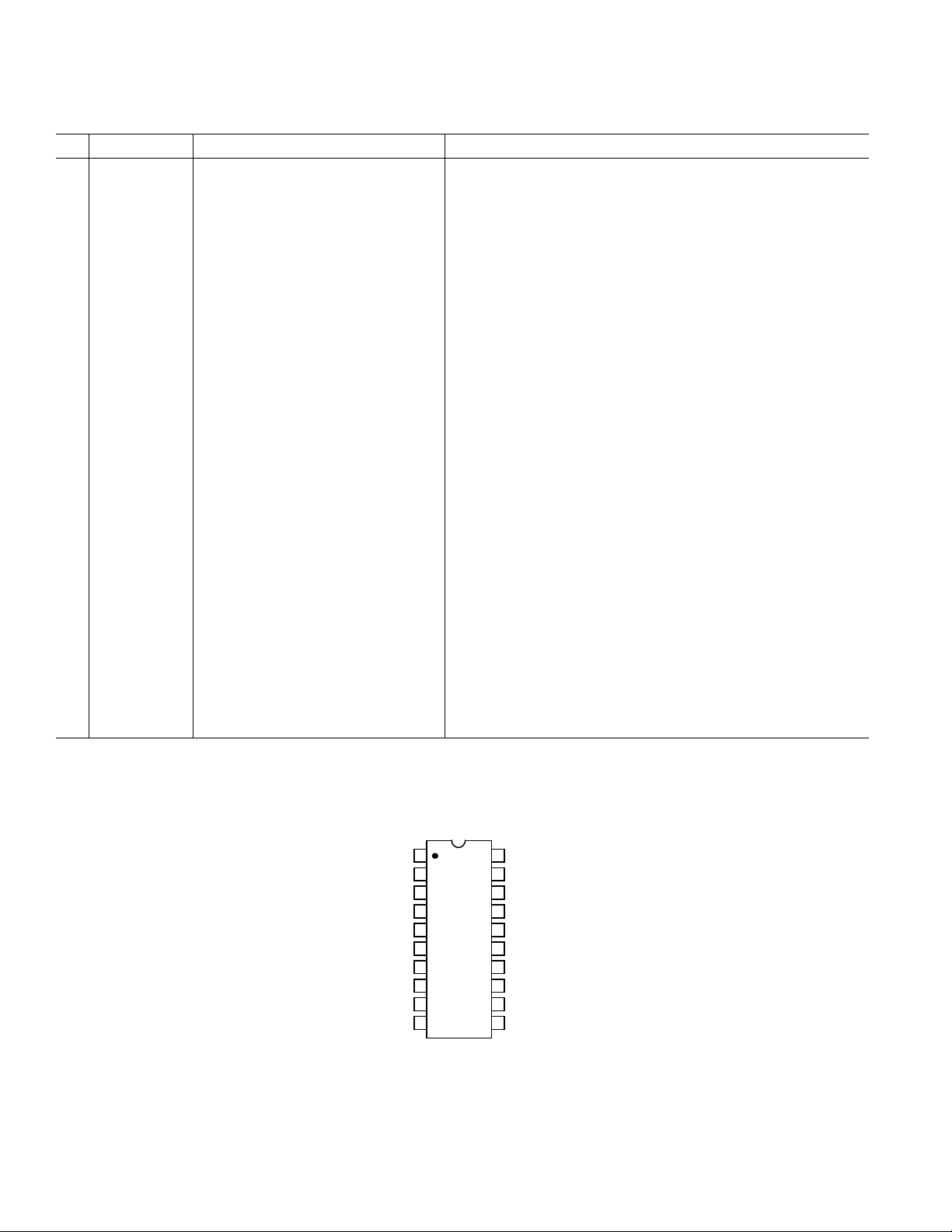
PIN FUNCTION DESCRIPTIONS
Pin Mnemonic Reads Function
1 FDIN Frequency Detector Input PLL Input for I/Q Demodulator Quadrature Oscillator, ±400 mV
Drive Required from External Oscillator. Must be biased at VP/2.
2 COM1 Common #1 Supply Common for RF Front End and Main Bias
3 PRUP Power-Up Input 3 V/5 V CMOS compatible power-up control; logical high =
powered-up; max input level = VPS1 = VPS2.
4 LOIP Local Oscillator Input LO input, ac-coupled ±54 mV LO input is required (–16 dBm for
50 Ω input termination).
5 RFLO RF “Low” Input Usually Connected to AC Ground
6 RFHI RF “High” Input AC-Coupled, ±56 mV, Max RF Input for Linear Operation
7 GREF Gain Reference Input High Impedance Input, typically 1.5 V, sets gain scaling.
8 MXOP Mixer Output High Impedance, Single-Sided Current Output, ±1.3 V Max
Voltage Output (±6 mA Max Current Output)
9 VMID Midsupply Bias Voltage Output of the Midsupply Bias Generator (VMID = VPOS/2)
10 IFHI IF “High” Input AC-Coupled IF Input, ± 56 mV Max Input for Linear Operation
11 IFLO IF “Low” Input Reference Node for IF Input; Auto-Offset Null
12 GAIN Gain Control Input High Impedance Input, 0 V–2 V Using 3 V Supply, Max Gain at
V = 0
13 COM2 Common #2 Supply Common for IF Stages and Demodulator
14 IFOP IF Output Low Impedance, Single-Sided Voltage Output, 5 dBm
(± 560 mV) Max
15 DMIP Demodulator Input Signal input to I and Q demodulators has a ±150 mV max input
at IF > 3 MHz for linear operation; ±75 mV max input at IF < 3 MHz
for linear operation. Must be biased at VP/2.
16 VPS2 VPOS Supply #2 Supply to High Level IF, PLL, and Demodulators
17 QOUT Quadrature Output Low Impedance Q Baseband Output; ± 1.23 V Full Scale in 20 kΩ
Min Load; AC-Coupled
18 IOUT In-Phase Output Low Impedance I Baseband Output; ±1.23 V Full Scale in 20 kΩ
Min Load; AC-Coupled
19 FLTR PLL Loop Filter Series RC PLL Loop Filter, Connected to Ground
20 VPS1 VPOS Supply #1 Supply to Mixer, Low Level IF, PLL, and Gain Control
PIN CONNECTION
20-Lead SSOP (RS-20)
FDIN
COM1
PRUP
LOIP
RFLO
RFHI
GREF
MXOP
VMID
IFHI
1
2
3
4
5
AD607
TOP VIEW
6
(Not to Scale)
7
8
9
10
20
VPS1
19
FLTR
18
IOUT
17
QOUT
16
VPS2
15
DMIP
14
IFOP
13
COM2
12
GAIN
11
IFLO
–4–
REV. C
HP8656B
IEEE
RF_OUT
SYNTHESIZER
HP8656B
IEEE
RF_OUT
SYNTHESIZER
HP8656B
IEEE
RF_OUT
SYNTHESIZER
HP6633A
IEEE
VPOS
VNEG
SPOS
SNEG
DCPS
HP34401A
CPIB
HI
LO
I
DMM
DP8200
IEEE
VPOS
VNEG
SPOS
SNEG
V
REF
HP8764B
0
0
1
1
S0
S1
V
50⍀
50⍀
MXOP
RFHI
LOIP
L
R
X
IFOPIFHI
PLL
IOUT
QOUT
DMIP
FDIN
BIAS
VPOS
PRUP
GAIN
HP8764B
0
0
1
1
S0
S1
V
50⍀
50⍀
HP8594E
RF_IN
IEEE
SPEC
AN
HP8765B
0
1
C
S0
S1V
R5
1k⍀
CHARACTERIZATION
BOARD
HP8765B
0
1C
S0 S1V
P6205
X10
OUT
FET PROBE
TEK1105
IN1 OUT1
IN2 OUT2
PROBE
SUPPLY
AD607
REV. C
HP8720C
IEEE_488
NETWORK AN
HP346B
28V
NOISE SOURCE
HP8656B
IEEE
SYNTHESIZER
HP6633A
IEEE
DCPS
DP8200
IEEE
V
REF
PORT_1
PORT_2
NOISE
RF_OUT
VPOS
VNEG
SPOS
SNEG
VPOS
VNEG
SPOS
SNEG
HP8765B
0
1C
S0 S1
V
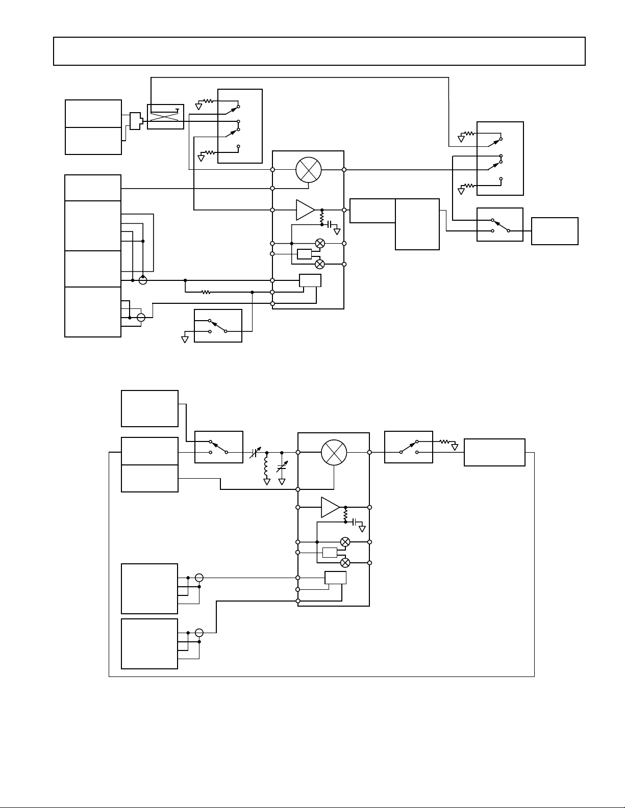
Figure 1. Mixer/Amplifier Test Set
CHARACTERIZATION
BOARD
RFHI
LOIP
DMIP
FDIN
VPOS
PRUP
GAIN
Figure 2. Mixer Noise Figure Test Set
X
R
L
PLL
BIAS
MXOP
IFOPIFHI
IOUT
QOUT
C
–5–
HP8765B
S1 V
50⍀
0
1
S0
RF_IN 28V_OUT
NOISE FIGURE METER
HP8970A
AD607
CHARACTERIZATION
BOARD
HP8656B
IEEE
DCFM
IEEE
DUAL SYNTHESIZER
IEEE
IEEE
RF_OUT
SYNTHESIZER
HP3326A
OUTPUT_1
OUTPUT_2
HP6633A
DCPS
DP8200
V
REF
VPOS
VNEG
SPOS
SNEG
VPOS
VNEG
SPOS
SNEG
HP346B
28V
NOISE SOURCE
HP6633A
IEEE
DCPS
DP8200
IEEE
V
REF
50⍀
50⍀
NOISE
VPOS
VNEG
SPOS
SNEG
VPOS
VNEG
SPOS
SNEG
HP8764B
RFHI
LOIP
DMIP
FDIN
VPOS
PRUP
GAIN
R
PLL
L
BIAS
MXOP
X
IFOPIFHI
IOUT
QOUT
X10
FET
P6205
OUT
PROBE
TEK1103
IN1 OUT1
IN2 OUT2
PROBE SUPPLY
HP8970A
RF_IN 28V_OUT
NOISE FIGURE METER
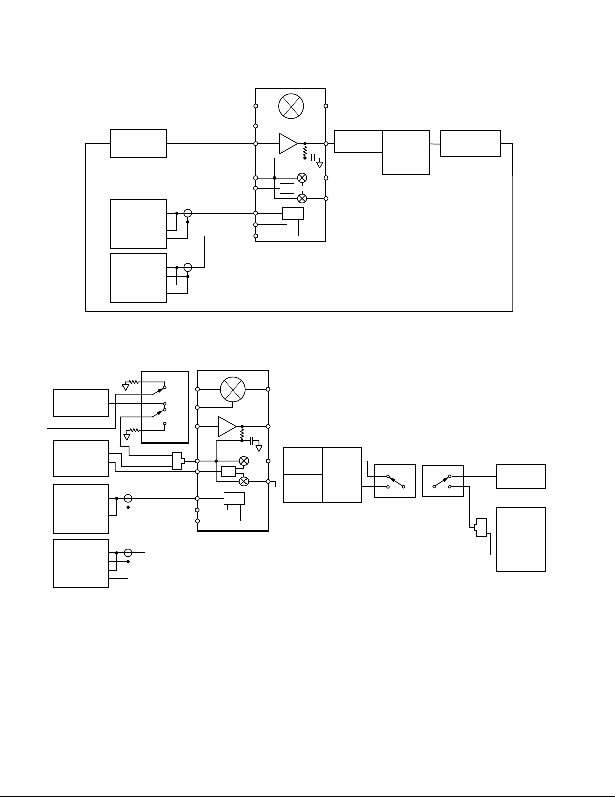
Figure 3. IF Amp Noise Figure Test Set
CHARACTERIZATION
BOARD
0
1
0
1
RFHI
LOIP
S0
S1
V
DMIP
FDIN
VPOS
PRUP
GAIN
MXOP
X
R
L
IFOPIFHI
OUT
OUT
IN1
IN2
1103
PROBE
SUPPLY
OUT1
OUT2
HP8765B
0
1C
S0
S1V
HP8765B
C
0
1
S0S1
V
HP8694E
RF_IN
CH1
CH2
CH3
CH4
TRIG IEEE_488
OSCILLOSCOPE
SPEC AN
HP54120
DIGITAL
IEEE
PLL
BIAS
IOUT
QOUT
P6205
X10
FET PROBE
P6205
X10
FET PROBE
Figure 4. PLL/Demodulator Test Set
–6–
REV. C
IEEE
IEEE
GPIB
HP6633A
DCPS
DP8200
V
REF
HP34401A
DMM
VPOS
VNEG
SPOS
SNEG
VPOS
VNEG
SPOS
SNEG
HI
LO
I
499k
R1
⍀
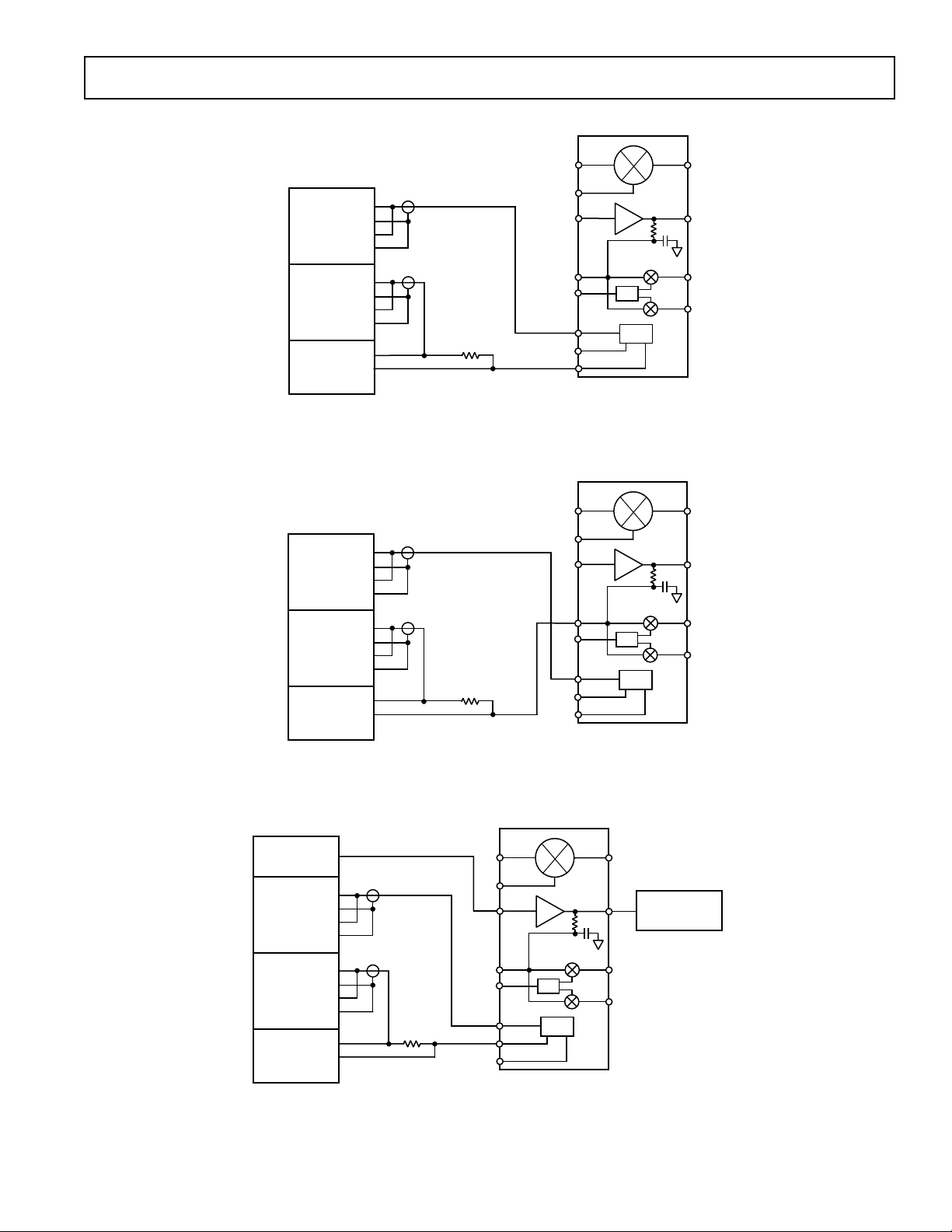
Figure 5. GAIN Pin Bias Test Set
CHARACTERIZATION
BOARD
R
LOIP
IFHI
DMIP
FDIN
VPOS
PRUP
GAIN
L
PLL
BIAS
CHARACTERIZATION
BOARD
AD607
MXOPRFHI
X
IFOP
IOUT
QOUT
HP3325B
IEEE
SYNTHESIZER
HP6633A
IEEE
DCPS
HP6633A
IEEE
DCPS
HP34401A
GPIB
DMM
IEEE
IEEE
GPIB
HP6633A
DCPS
DP8200
V
HP34401A
DMM
RF_OUT
VPOS
VNEG
SPOS
SNEG
VPOS
VNEG
SPOS
SNEG
VPOS
VNEG
SPOS
SNEG
VPOS
VNEG
SPOS
SNEG
REF
HI
LO
I
R1
499k⍀
Figure 6. Demodulator Bias Test Set
CHARACTERIZATION
RFHI
LOIP
IFHI
DMIP
FDIN
R1
HI
LO
I
10k⍀
VPOS
PRUP
GAIN
BOARD
R
L
PLL
BIAS
R
PLL
BIAS
L
X
RF_IN
MXOP
IFOP
IOUT
QOUT
HP8594E
IEEE
SPEC AN
RFHI
LOIP
IFHI
DMIP
FDIN
VPOS
PRUP
GAIN
MXOP
X
IFOP
IOUT
QOUT
REV. C
Figure 7. Power-Up Threshold Test Set
–7–
AD607
CHARACTERIZATION
BOARD
FL6082A
MOD_OUT
HP6633A
DCPS
DP8200
V
REF
HP8112
PULSE_OUT
RF_OUT
VPOS
VNEG
SPOS
SNEG
VPOS
VNEG
SPOS
SNEG
IEEE
IEEE
IEEE
IEEE
PULSE GENERATOR
RFHI
LOIP
IFHI
MXOP
R
X
L
IFOP
50⍀
DMIP
FDIN
VPOS
PRUP
GAIN
PLL
IOUT
QOUT
BIAS
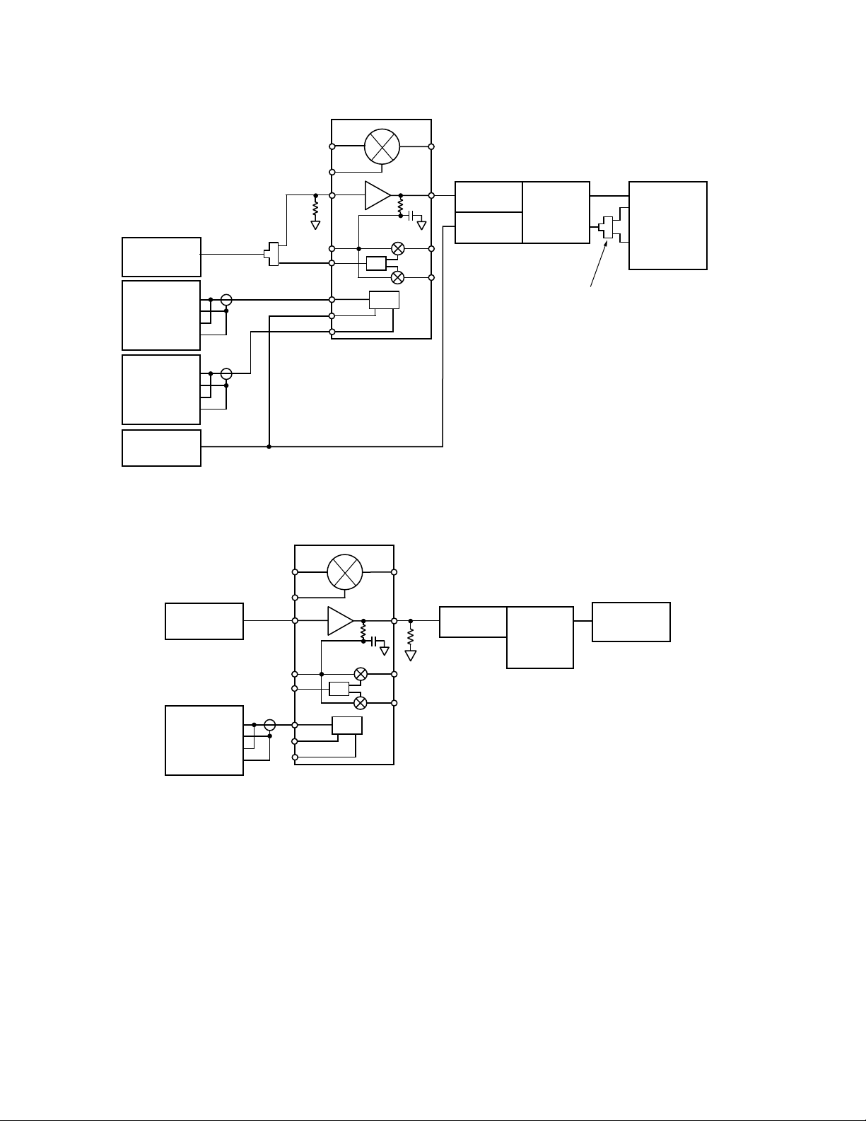
Figure 8. Power-Up Test Set
CHARACTERIZATION
BOARD
X10
FET PROBE
X10
FET PROBE
P6205
P6205
OUT
OUT
IN1
IN2
1103
OUT1
OUT2
PROBE SUPPLY
HP54120
CH1
CH2
CH3
CH4
TRIG
DIGITAL
OSCILLOSCOPE
NOTE: MUST BE 3 RESISTOR POWER DIVIDER
IEEE_488
HP8656B
SYNTHESIZER
HP6633A
IEEE
DCPS
MXOPRFHI
R
X
PLL
L
BIAS
IFOP
IOUT
QOUT
R1
1k⍀
P6205
X10
FET PROBE
OUT
IN1 OUT1
IN2 OUT2
PROBE SUPPLY
1103
RF_IN
HP8594E
IEEE
SPEC AN
LOIP
RF_OUTIEEE
VPOS
VNEG
SPOS
SNEG
IFHI
DMIP
FDIN
VPOS
PRUP
GAIN
Figure 9. IF Output Impedance Test Set
–8–
REV. C
 Loading...