Analog Devices AD605BR-REEL7, AD605BR-REEL, AD605BR, AD605BN, AD605AR-REEL7 Datasheet
...
Dual, Low Noise, Single-Supply
PRECISION PASSIVE
INPUT ATTENUATOR
FIXED GAIN
AMPLIFIER
+34.4dB
DIFFERENTIAL
ATTENUATOR
0 TO –48.4dB
OUT
VOCM
VGN
VREF
+IN
–IN
GAIN
CONTROL
AND
SCALING
FBK
AD605
a
FEATURES
Two Independent Linear-in-dB Channels
Input Noise at Maximum Gain: 1.8 nV/√Hz, 2.7 pA/√Hz
Bandwidth: 40 MHz (–3 dB)
Differential Input
Absolute Gain Range Programmable:
–14 dB to +34 dB (FBK Shorted to OUT), through
0 dB to +48 dB (FBK Open)
Variable Gain Scaling: 20 dB/V through 40 dB/V
Stable Gain with Temperature and Supply Variations
Single-Ended Unipolar Gain Control
Output Common-Mode Independently Set
Power Shutdown at Lower End of Gain Control
Single 5 V Supply
Low Power: 90 mW/Channel
Drives A/D Converters Directly
APPLICATIONS
Ultrasound and Sonar Time-Gain Control
High Performance AGC Systems
Signal Measurement
Variable Gain Amplifier
AD605
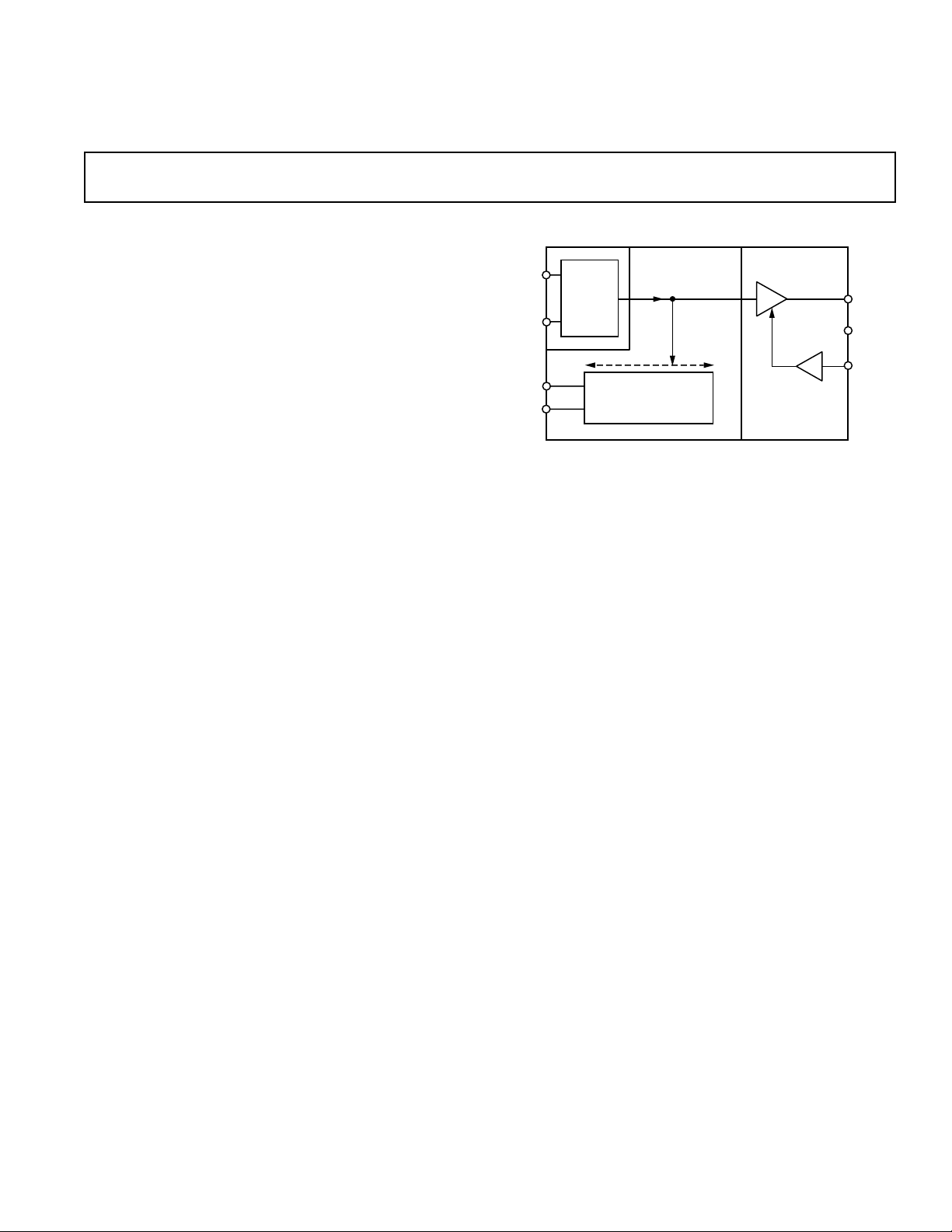
FUNCTIONAL BLOCK DIAGRAM
PRODUCT DESCRIPTION
The AD605 is a low noise, accurate, dual channel, linear-in-dB
variable gain amplifier, which is optimized for any application
requiring high performance, wide bandwidth variable gain control. Operating from a single 5 V supply, the AD605 provides
differential inputs and unipolar gain control for ease of use.
Added flexibility is achieved with a user determined gain range
and an external reference input which provides user determined
gain scaling (dB/V).
The high performance linear-in-dB response of the AD605 is
achieved with the differential input, single supply, exponential
amplifier (DSX-AMP) architecture. Each of the DSX-AMPs
comprise a variable attenuator of 0 dB to –48.4 dB followed by
a high speed fixed gain amplifier. The attenuator is based on a
7-stage R-1.5-R ladder network. The attenuation between tap
points is 6.908 dB and 48.360 dB for the entire ladder network.
The DSX-AMP architecture results in 1.8 nV/√Hz input noise
spectral density and will accept a ±2.0 V input signal when
VOCM is biased at VP/2.
Each independent channel of the AD605 provides a gain range
of 48 dB which can be optimized for the application. Gain
REV. B
Information furnished by Analog Devices is believed to be accurate and
reliable. However, no responsibility is assumed by Analog Devices for its
use, nor for any infringements of patents or other rights of third parties that
may result from its use. No license is granted by implication or otherwise
under any patent or patent rights of Analog Devices.
ranges between –14 dB to +34 dB and 0 dB to +48 dB can be
selected by a single resistor between pins FBK and OUT. The
lower and upper gain range are determined by shorting pin FBK
to OUT, or leaving pin FBK unconnected respectively. The two
channels of the AD605 can be cascaded to provide 96 dB of very
accurate gain range in a monolithic package.
The gain control interface provides an input resistance of approximately 2 MΩ and scale factors from 20 dB/V to 30 dB/V for a
VREF input voltage of 2.5 V to 1.67 V respectively. Note that
scale factors up to 40 dB are achievable with reduced accuracy
for scales above 30 dB. The gain scales linearly with control voltages (VGN) of 0.4 V to 2.4 V for the 20 dB/V scale and 0.20 V
to 1.20 V for the 40 dB/V scale. When VGN is <50 mV the
amplifier is powered-down to draw 1.9 mA. Under normal
operation, the quiescent supply current of each amplifier channel is only 18 mA.
The AD605 is available in a 16-lead plastic DIP and SOIC, and
is guaranteed for operation over the –40°C to +85°C temperature range.
One Technology Way, P.O. Box 9106, Norwood, MA 02062-9106, U.S.A.
Tel: 781/329-4700 www.analog.com
Fax: 781/326-8703 © Analog Devices, Inc., 2001

(Each Channel at TA = 25ⴗC, VS = 5 V, RS = 50 ⍀, RL = 500 ⍀, CL = 5 pF, VREF = 2.5 V
AD605–SPECIFICATIONS
Model AD605A AD605B
Parameter Conditions Min Typ Max Min Typ Max Unit
INPUT CHARACTERISTICS
Input Resistance 175 ± 40 175 ± 40 Ω
Input Capacitance 3.0 3.0 pF
Peak Input Voltage 2.5 ± 2.5 2.5 ± 2.5 V
Input Voltage Noise VGN = 2.9 V 1.8 1.8 nV/√Hz
Input Current Noise VGN
Noise Figure R
Common-Mode Rejection Ratio f = 1 MHz, VGN = 2.65 V –20 –20 dB
OUTPUT CHARACTERISTICS
–3 dB Bandwidth Constant with Gain 40 40 MHz
Slew Rate VGN = 1.5 V, Output = 1 V Step 170 170 V/µs
Output Signal Range R
Output Impedance f = 10 MHz 2 2 Ω
Output Short-Circuit Current ±40 ±40 mA
Harmonic Distortion VGN = 1 V, VOUT = 1 V p-p,
HD2 f = 1 MHz –64 –64 dBc
HD3 f = 1 MHz –68 –68 dBc
HD2 f = 10 MHz –51 –51 dBc
HD3 f = 10 MHz –53 –53 dBc
Two-Tone Intermodulation R
Distortion (IMD) f = 1 MHz –72 –72 dBc
1 dB Compression Point f = 10 MHz, VGN = 2.9 V, Output Referred +15 +15 dBm
Third Order Intercept f = 10 MHz, VGN = 2.9 V, VOUT = 1 V p-p, –1 –1 dBm
Channel-to-Channel Crosstalk Ch1: VGN = 2.65 V, Inputs Shorted, –70 –70 dB
Group Delay Variation 1 MHz < f < 10 MHz, Full Gain Range ± 2.0 ±2.0 ns
VOCM Input Resistance 45 45 kΩ
ACCURACY
Absolute Gain Error
–14 dB to –11 dB 0.25 V < VGN < 0.40 V –1.2 +1.0 +3.0 –1.2 +0.75 +3.0 dB
–11 dB to +29 dB 0.40 V < VGN < 2.40 V –1.0 ±0.3 +1.0 –1.0 ± 0.2 +1.0 dB
+29 dB to +34 dB 2.40 V < VGN < 2.65 V –3.5 –1.25 +1.2 –3.5 –1.25 +1.2 dB
Gain Scaling Error 0.4 V < VGN < 2.4 V ±0.25 ±0.25 dB/V
Output Offset Voltage VREF
Output Offset Variation VREF = 2.500 V, VOCM = 2.500 V 30 95 30 50 mV
GAIN CONTROL INTERFACE
Gain Scaling Factor VREF = 2.5 V, 0.4 V < VGN < 2.4 V 19 20 21 19 20 21 dB/V
Gain Range FBK Short to OUT –14 – +34 –14 – +34 dB
Input Voltage (VGN) Range 20 dB/V, VREF = 2.5 V 0.1 – 2.9 0.1 – 2.9 V
Input Bias Current –0.4 –0.4 µA
Input Resistance 22MΩ
Response Time 48 dB Gain Change 0.2 0.2 µs
POWER SUPPLY
Power Dissipation 90 90 mW
VREF Input Resistance 10 10 kΩ
Quiescent Supply Current VPOS 18 23 18 23 mA
Power Down VPOS, VGN < 50 mV 1.9 3.0 1.9 3.0 mA
Power-Up Response Time 48 dB Gain, V
Power-Down Response Time 0.4 0.4 µs
= 2.9 V 2.7 2.7 pA/√Hz
= 50 Ω, f = 10 MHz at Minimum Gain, 8.4 8.4 dB
S
VGN = 2.9 V
= 200 Ω, f = 10 MHz at Minimum Gain, 12 12 dB
R
S
VGN = 2.9 V
≥ 500 Ω 2.5 ± 1.5 2.5 ± 1.5 V
L
= 0 Ω, VGN = 2.9 V, VOUT = 1 V p-p
S
f = 10 MHz –60 –60 dBc
Input Referred
Ch2: VGN = 1.5 V (Mid Gain), f = 1 MHz,
VOUT = 1 V p-p
= 2.500 V, VOCM = 2.500 V –50 ±30 50 –50 ±30 50 mV
VREF = 1.67 V 30 30 dB/V
FBK Open 0 – +48 0 – +48 dB
(Scaling = 20 dB/V), –14 dB to +34 dB gain range, unless otherwise noted.)
= 2 V p-p 0.6 0.6 µs
OUT
–2–
REV. B

AD605
WARNING!
ESD SENSITIVE DEVICE
ABSOLUTE MAXIMUM RATINGS*
Supply Voltage +V
S
Pins 12, 13 (with Pins 4, 5 = 0 V) . . . . . . . . . . . . . . . 6.5 V
Input Voltages Pins 1–3, 6–9, 16 . . . . . . . . . . . . . . . VPOS, 0
Internal Power Dissipation
Plastic (N) . . . . . . . . . . . . . . . . . . . . . . . . . . . . . . . . . 1.4 W
Small Outline (R) . . . . . . . . . . . . . . . . . . . . . . . . . . . . 1.2 W
Operating Temperature Range . . . . . . . . . . . –40°C to +85°C
Storage Temperature Range . . . . . . . . . . . . –65°C to +150°C
Lead Temperature, Soldering 60 seconds . . . . . . . . . . 300°C
*Stresses above those listed under Absolute Maximum Ratings may cause perma-
nent damage to the device. This is a stress rating only; functional operation of the
device at these or any other conditions above those indicated in the operational
section of this specification is not implied. Exposure to absolute maximum rating
conditions for extended periods may affect device reliability.
ORDERING GUIDE
Model Temperature Range Package Description Package Option
AD605AN –40°C to +85°C Plastic DIP N-16 85°C/W
AD605AR –40°C to +85°C Small Outline IC (SOIC) R-16A 100°C/W
AD605BN –40°C to +85°C Plastic DIP N-16 85°C/W
AD605BR –40°C to +85°C Small Outline IC (SOIC) R-16A 100°C/W
AD605ACHIPS DIE
AD605AR-REEL 13" Reel
AD605AR-REEL7 7" Reel
AD605BR-REEL 13" Reel
AD605BR-REEL7 7" Reel
AD605-EB Evaluation Board
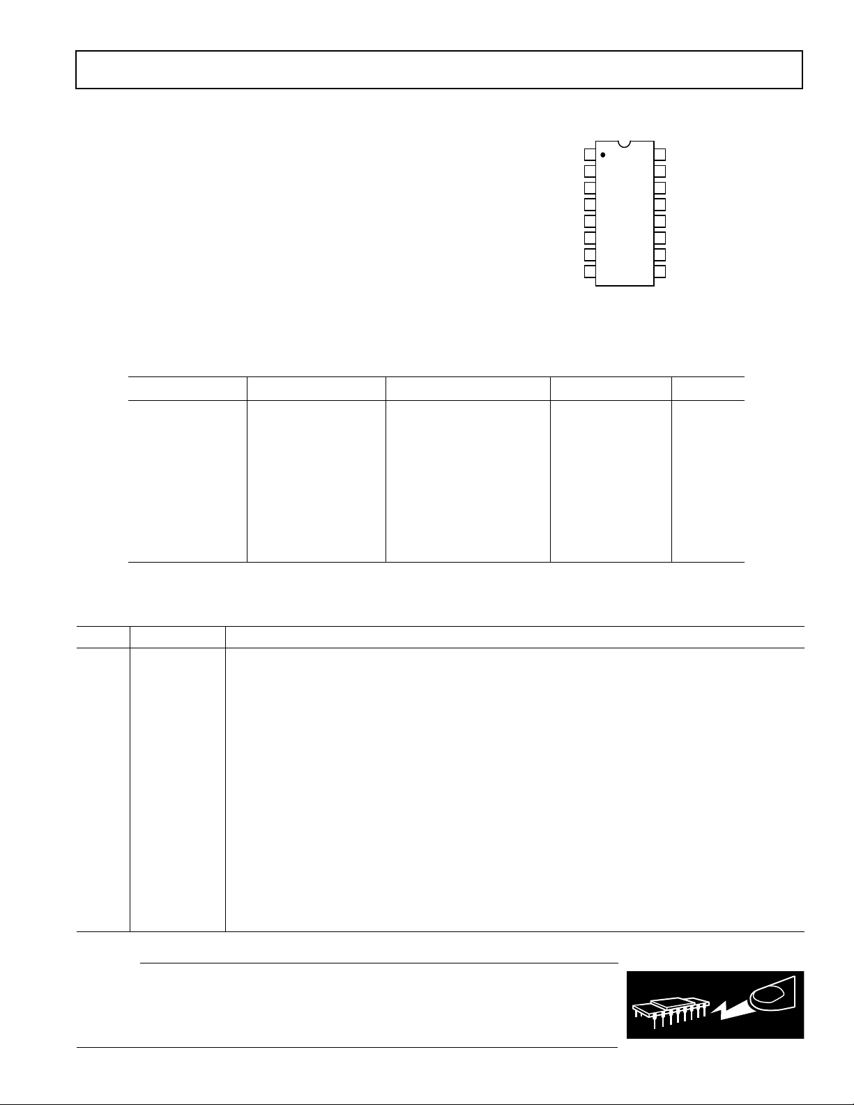
PIN CONFIGURATION
VGN1
–IN1
+IN1
GND1
GND2
+IN2
–IN2
VGN2
1
2
3
AD605
4
TOP VIEW
5
(Not to Scale)
6
7
8
16
15
14
13
12
11
10
9
VREF
OUT1
FBK1
VPOS
VPOS
FBK2
OUT2
VOCM
JA
PIN FUNCTION DESCRIPTIONS
16-Lead Package for Dual Channel AD605
Pin No. Mnemonic Description
1 VGN1 CH1 Gain-Control Input and Power-Down Pin. If grounded, device is off, otherwise positive voltage
increases gain.
2 –IN1 CH1 Negative Input.
3 +IN1 CH1 Positive Input.
4 GND1 Ground.
5 GND2 Ground.
6 +IN2 CH2 Positive Input.
7 –IN2 CH2 Negative Input.
8 VGN2 CH2 Gain-Control Input and Power-Down Pin. If grounded, device is off, otherwise positive voltage
increases gain.
9 VOCM Input to this pin defines common-mode voltage for OUT1 and OUT2.
10 OUT2 CH2 Output.
11 FBK2 Feedback Pin that Selects Gain Range of CH2.
12 VPOS Positive Supply.
13 VPOS Positive Supply.
14 FBK1 Feedback Pin that Selects Gain Range of CH1.
15 OUT1 CH1 Output.
16 VREF Input to this pin sets gain-scaling for both channels: 2.5 V = 20 dB/V, 1.67 V = 30 dB/V.
CAUTION
ESD (electrostatic discharge) sensitive device. Electrostatic charges as high as 4000 V readily
accumulate on the human body and test equipment and can discharge without detection. Although
the AD605 features proprietary ESD protection circuitry, permanent damage may occur on devices
subjected to high-energy electrostatic discharges. Therefore, proper ESD precautions are
recommended to avoid performance degradation or loss of functionality.
REV. B
–3–

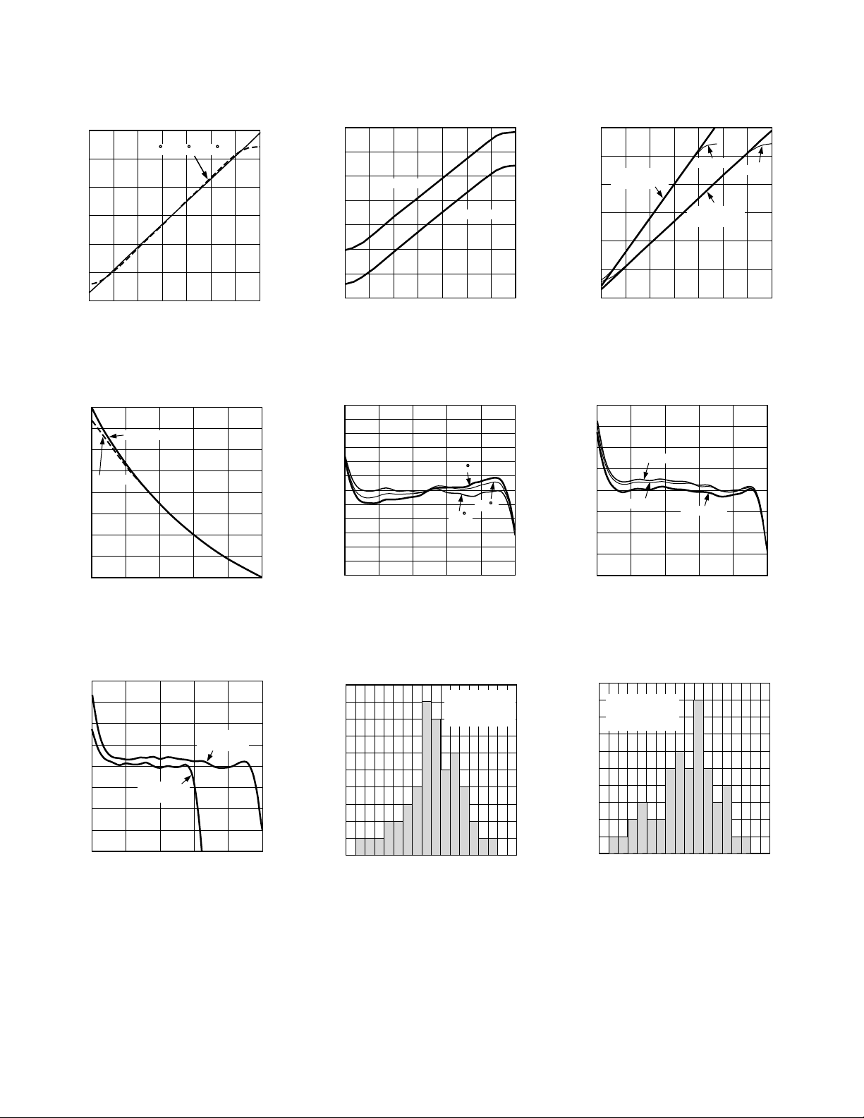
AD605–Typical Performance Characteristics (per Channel)
(V
= 2.5 V (20 dB/V Scaling), f = 1 MHz, RL = 500 ⍀, CL = 5 pF, TA = 25ⴗC, VSS = 5 V)
REF
40
30
20
10
GAIN – dB
0
–10
–20
0.1 0.5 2.9
–40 C, +25 C, +85 C
0.9 1.3 1.7 2.1 2.5
VGN – Volts
TPC 1. Gain vs. VGN
40.0
37.5
35.0
32.5
30.0
27.5
25.0
GAIN SCALING – dBV
22.5
20.0
1.25 1.50 2.50
ACTUAL
THEORETICAL
1.75 2.00 2.25
V
REF
– Volts
TPC 4. Gain Scaling vs. V
REF
50
40
GAIN – dB
–10
–20
30
20
10
FBK (OPEN)
FBK (SHORT)
0
0.1 0.5 2.9
0.9 1.3 1.7 2.1 2.5
VGN – Volts
TPC 2. Gain vs. VGN for Different
Gain Ranges
3.0
2.5
2.0
1.5
1.0
0.5
0.0
–0.5
–1.0
GAIN ERROR – dB
–1.5
–2.0
–2.5
–3.0
0.2 0.7 2.7
1.2 1.7 2.2
VGN –Volts
–40 C
+85 C
+25 C
TPC 5. Gain Error vs. VGN at
Different Temperatures
40
30
30dB/V
= 1.67V)
(V
REF
20
10
GAIN – dB
0
–10
–20
0.1 0.5 2.9
0.9 1.3 1.7 2.1 2.5
ACTUAL
20dB/V
(V
REF
VGN – Volts
ACTUAL
= 2.50V)
TPC 3. Gain vs. VGN for Different
Gain Scalings
2.0
1.5
1.0
0.5
0.0
–0.5
GAIN ERROR – dB
–1.0
–1.5
–2.0
0.2 0.7 2.7
f = 1MHz
f = 5MHz
1.2 1.7 2.2
VGN – Volts
f = 10MHz
TPC 6. Gain Error vs. VGN at
Different Frequencies
2.0
1.5
1.0
0.5
0.0
–0.5
GAIN ERROR – dB
–1.0
–1.5
–2.0
0.2 0.7 2.71.2 1.7 2.2
30dB/V
V
= 1.67V
REF
VGN – Volts
V
REF
20dB/V
= 2.50V
TPC 7. Gain Error vs. VGN for
Different Gain Scalings
20
18
16
14
12
10
8
PERCENTAGE
6
4
2
0
–0.8 –0.6 –0.4 –0.2 0.0 0.2 0.4
DELTA GAIN – dB
N = 50
⌬G(dB) =
G(CH1) – G(CH2)
0.6 0.8
TPC 8. Gain Match, VGN1 = VGN2 =
1.0 V
–4–
20
18
N = 50
⌬G(dB) =
16
G(CH1) – G(CH2)
14
12
10
8
PERCENTAGE
6
4
2
0
–0.8 –0.6 –0.4 –0.2 0.0 0.2 0.4 0.6 0.8
DELTA GAIN – dB
TPC 9. Gain Match, VGN1 = VGN2 =
2.50 V
REV. B
 Loading...