Dual, Ultralow Noise
a
FEATURES
Ultralow Input Noise at Maximum Gain:
0.80 nV/√Hz, 3.0 pA/√Hz
Two Independent Linear-in-dB Channels
Absolute Gain Range per Channel Programmable:
0 dB to +48 dB (Preamp Gain = +14 dB), through
+6 dB to +54 dB (Preamp Gain = +20 dB)
61.0 dB Gain Accuracy
Bandwidth: 40 MHz (–3 dB)
300 kV Input Resistance
Variable Gain Scaling: 20 dB/V through 40 dB/V
Stable Gain with Temperature and Supply Variations
Single-Ended Unipolar Gain Control
Power Shutdown at Lower End of Gain Control
Can Drive A/D Converters Directly
APPLICATIONS
Ultrasound and Sonar Time-Gain Control
High Performance AGC Systems
Signal Measurement
PAI
PROGRAMMABLE
ULTRALOW NOISE
PREAMPLIFIER
G = 14–20dB
Variable Gain Amplifier
AD604
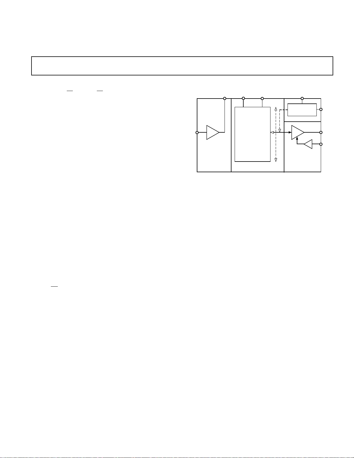
FUNCTIONAL BLOCK DIAGRAM
PAO
–DSX
LADDER NETWORK
PRECISION PASSIVE
INPUT ATTENUATOR
+DSX
DIFFERENTIAL
ATTENUATOR
R-1.5R
0 TO –48.4dB
VGN
GAIN CONTROL
AND SCALING
AFA
FIXED GAIN
AMPLIFIER
+34.4dB
VREF
OUT
VOCM
PRODUCT DESCRIPTION
The AD604 is an ultralow noise, very accurate, dual channel,
linear-in-dB variable gain amplifier (VGA) optimized for timebased variable gain control in ultrasound applications; however
it will support any application requiring low noise, wide bandwidth
variable gain control. Each channel of the AD604 provides a
300 kΩ input resistance and unipolar gain control for ease of
use. User determined gain ranges, gain scaling (dB/V) and dc
level shifting of output further optimize application performance.
Each channel of the AD604 utilizes a high performance preamplifier that provides an input referred noise voltage of
0.8 nV/√
Hz. The very accurate linear-in-dB response of the
AD604 is achieved with the differential input exponential amplifier
(DSX-AMP) architecture. Each of the DSX-AMPs comprise a
variable attenuator of 0 dB to 48.36 dB followed by a high speed
fixed gain amplifier. The attenuator is based on a seven stage
R-1.5R ladder network. The attenuation between tap points
is 6.908 dB and 48.36 dB for the ladder network.
Each independent channel of the AD604 provides a gain range
of 48 dB which can be optimized for the application by programming the preamplifier with a single external resistor in the
preamp feedback path. The linear-in-dB gain response of the
AD604 can be described by the equation: G (dB) = (Gain
Scaling (dB/V) × VGN (V)) + (Preamp Gain (dB) – 19 dB).
Preamplifier gains between 5 and 10 (+14 dB and +20 dB)
provide overall gain ranges per channel of 0 dB through +48 dB
and +6 dB through +54 dB. The two channels of the AD604
can be cascaded to provide greater levels of gain range by bypassing the 2nd channel’s preamplifier. However, in multiple channel
systems, cascading the AD604 with other devices in the AD60x
VGA family, which do not include a preamplifier may provide
a more efficient solution. The AD604 provides access to the
output of the preamplifier allowing for external filtering between the preamplifier and the differential attenuator stage.
The gain control interface provides an input resistance of
approximately 2 MΩ and scale factors from 20 dB/V to
30 dB/V for a V
input voltage of 2.5 V to 1.67 V respect-
REF
ively. Note that scale factors up to 40 dB/V are achievable
with reduced accuracy for scales above 30 dB/V. The gain scales
linear-in-dB with control voltages of 0.4 V to 2.4 V with the
20 dB/V scale. Below and above this gain control range, the gain
begins to deviate from the ideal linear-in-dB control law. The
gain control region below 0.1 V is not used for gain control. In
fact when the gain control voltage is <50 mV the amplifier
channel is powered down to 1.9 mA.
The AD604 is available in a 24-pin plastic SSOP, SOIC and DIP,
and is guaranteed for operation over the –40°C to +85°C
temperature range.
REV. 0
Information furnished by Analog Devices is believed to be accurate and
reliable. However, no responsibility is assumed by Analog Devices for its
use, nor for any infringements of patents or other rights of third parties
which may result from its use. No license is granted by implication or
otherwise under any patent or patent rights of Analog Devices.
One Technology Way, P.O. Box 9106, Norwood, MA 02062-9106, U.S.A.
Tel: 617/329-4700 World Wide Web Site: http://www.analog.com
Fax: 617/326-8703 © Analog Devices, Inc., 1996

AD604–SPECIFICATIONS
(Each Amplifier Channel at TA = +258C, VS = 65 V, RS = 50 V, RL = 500 V, CL = 5 pF, V
range (preamplifier gain = +14 dB), VOCM = 2.5 V, C1 and C2 = 0.1 mF (see Figure 35) unless otherwise noted)
Parameter Conditions Min Typ Max Unit
INPUT CHARACTERISTICS
Preamplifier
Input Resistance 300 kΩ
Input Capacitance 8.5 pF
Input Bias Current –27 µA
Peak Input Voltage Preamp Gain = +14 dB ±400 mV
Preamp Gain = +20 dB ±200 mV
Input Voltage Noise VGN
= 2.9 V, R
= 0 Ω
S
Preamp Gain = +14 dB 0.8 nV/√
Preamp Gain = +20 dB 0.73 nV/√
Input Current Noise Independent of Gain 3.0 pA/√
Noise Figure R
= 50 Ω, f = 1 MHz, VGN = 2.9 V 2.3 dB
S
R
= 200 Ω, f =1 MHz, VGN
S
= 2.9 V 1.1 dB
DSX
Input Resistance 175 Ω
Input Capacitance 3.0 pF
Peak Input Voltage 2.5 ± 2V
Input Voltage Noise VGN
Input Current Noise VGN
Noise Figure R
= 2.9 V 1.8 nV/√Hz
= 2.9 V 2.7 pA/√Hz
= 50 Ω, f = 1 MHz, VGN = 2.9 V 8.4 dB
S
R
= 200 Ω, f =1 MHz, VGN
S
= 2.9 V 12 dB
Common-Mode Rejection Ratio f = 1 MHz, VGN = 2.65 V –20 dB
= 2.50 V (Scaling = 20 dB/V), 0 dB to +48 dB gain
REF
Hz
Hz
Hz
OUTPUT CHARACTERISTICS
–3 dB Bandwidth Constant with Gain 40 MHz
Slew Rate VGN = 1.5 V, Output = 1 V Step 170 V/µs
Output Signal Range R
≥ 500 Ω 2.5 ± 1.5 V
L
Output Impedance f = 10 MHz 2 Ω
Output Short-Circuit Current ±40 mA
Harmonic Distortion VGN
= 1 V, V
OUT
= 1 V p-p
HD2 f = 1 MHz –54 dBc
HD3 f = 1 MHz –67 dBc
HD2 f = 10 MHz –43 dBc
HD3 f = 10 MHz –48 dBc
Two-Tone Intermodulation VGN = 2.9 V, V
= 1 V p-p
OUT
Distortion (IMD) f = 1 MHz –74 dBc
f = 10 MHz –71 dBc
3rd Order Intercept f = 10 MHz, VGN
V
= 1 V p-p, Input Referred
OUT
1 dB Compression Point f = 1 MHz, VGN
Channel-to-Channel Crosstalk V
= 1 V p-p, f = 1 MHz
OUT
= 2.65 V, –12.5 dBm
= 2.9 V, Output Referred +15 dBm
Ch #1: VGN = 2.65 V, Inputs Shorted –30 dB
Ch #2: VGN = 1.5 V (Mid Gain) dB
Group Delay Variation 1 MHz < f < 10 MHz, Full Gain Range ±2ns
V
Input Resistance 45 kΩ
OCM
ACCURACY
Absolute Gain Error
0 dB to +3 dB 0.25 V < VGN < 0.400 V –1.2 +0.75 +3 dB
+3 dB to +43 dB 0.400 V < VGN < 2.400 V –1.0 ±0.3 +1.0 dB
+43 dB to +48 dB 2.400 V < VGN < 2.65 V –3.5 –1.25 +1.2 dB
Gain Scaling Error 0.400 V < VGN < 2.400 V ±0.25 dB/V
Output Offset Voltage V
Output Offset Variation V
= 2.500 V, V
REF
= 2.500 V, V
REF
= 2.500 V –50 ±30 +50 mV
OCM
= 2.500 V 30 50 mV
OCM
–2–
REV. 0

AD604
WARNING!
ESD SENSITIVE DEVICE
Parameter Conditions Min Typ Max Unit
GAIN CONTROL INTERFACE
Gain Scaling Factor V
Gain Range Preamp Gain = +14 dB 0 to +48 dB
Input Voltage (VGN) Range 20 dB/V, V
Input Bias Current –0.4 µA
Input Resistance 2MΩ
Response Time 48 dB Gain Change 0.2 µs
V
Input Resistance 10 kΩ
REF
POWER SUPPLY
Specified Operating Range One Complete Channel ±5V
Power Dissipation One Complete Channel 220 mW
Quiescent Supply Current VPOS, One Complete Channel 32 36 mA
Powered Down VPOS, VGN < 50 mV, One Channel 1.9 3.0 mA
Power-Up Response Time 48 dB Gain Change, V
Power-Down Response Time 0.4 µs
= 2.5 V, 0.4 V < VGN < 2.4 V 19 20 21 dB/V
REF
= 1.67 V 30 dB/V
V
REF
Preamp Gain = +20 dB +6 to +54 dB
= 2.5 V 0.1 to 2.9 V
REF
One DSX Only +5 V
One DSX Only 95 mW
VPOS, One DSX Only 19 23 mA
VNEG, One Preamplifier Only –15 –12 mA
VNEG, VGN < 50 mV, One Channel –150 µA
= 2 V p-p 0.6 µs
OUT
ABSOLUTE MAXIMUM RATINGS
Supply Voltage ±V
S
Pins 17, 18, 19, 20 (with Pins 16, 22 = 0 V) . . . . . . ±6.5 V
Input Voltages
Pins 1, 2, 11, 12 . . . . . . . . . . . . . VPOS/2 ±2 V Continuous
Pins 4, 9 . . . . . . . . . . . . . . . . . . . . . . . . . . . . . . . . . . . ±2 V
Pins 5, 8 . . . . . . . . . . . . . . . . . . . . . . . . . . . . VPOS, VNEG
Pins 6, 7, 13, 14, 23, 24 . . . . . . . . . . . . . . . . . . . . VPOS, 0
Internal Power Dissipation
Plastic (N) . . . . . . . . . . . . . . . . . . . . . . . . . . . . . . . . . 2.2 W
Model Range u
AD604AN –40°C to +85°C57°C/W N-24
AD604AR –40°C to +85°C70°C/W R-24
AD604ARS –40°C to +85°C 112°C/W R-24
*N = Plastic DIP, R = Small Outline IC (SOIC), RS = Shrink Small Outline
Package (SSOP).
ORDERING GUIDE
Temperature Package
Small Outline (R) . . . . . . . . . . . . . . . . . . . . . . . . . . . . 1.7 W
Shrink Small Outline (RS) . . . . . . . . . . . . . . . . . . . . . 1.1 W
Operating Temperature Range . . . . . . . . . . . –40°C to +85°C
Storage Temperature Range . . . . . . . . . . . . –65°C to +150°C
Lead Temperature, Soldering 60 seconds . . . . . . . . . +300°C
NOTES
1
Stresses above those listed under “Absolute Maximum Ratings” may cause
permanent damage to the device. This is a stress rating only and functional operation of the device at these or any other conditions above those indicated in the
operational section of this specification is not implied. Exposure to absolute maximum rating conditions for extended periods may affect device reliability.
2
Pins 1, 2, 11, 12, 13, 14, 23, 24 are part of a single-supply circuit and the part will
most likely be damaged if any of these pins are accidentally connected to VN.
3
When driven from an external low impedance source.
CAUTION
ESD (electrostatic discharge) sensitive device. Electrostatic charges as high as 4000 V readily
accumulate on the human body and test equipment and can discharge without detection.
Although the AD604 features proprietary ESD protection circuitry, permanent damage may
occur on devices subjected to high energy electrostatic discharges. Therefore, proper ESD
precautions are recommended to avoid performance degradation or loss of functionality.
JA
Option*
REV. 0
–3–

AD604
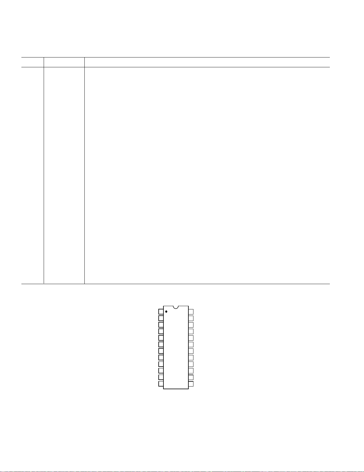
PIN DESCRIPTIONS
Pin No. Mnemonic Description
Pin 1 –DSX1 CH1 Negative Signal Input to DSX1.
Pin 2 +DSX1 CH1 Positive Signal Input to DSX1.
Pin 3 PAO1 CH1 Preamplifier Output.
Pin 4 FBK1 CH1 Preamplifier Feedback Pin.
Pin 5 PAI1 CH1 Preamplifier Positive Input.
Pin 6 COM1 CH1 Signal Ground; when connected to positive supply, Preamplifier1 will shut down.
Pin 7 COM2 CH2 Signal Ground; when connected to positive supply, Preamplifier2 will shut down.
Pin 8 PAI2 CH2 Preamplifier Positive Input.
Pin 9 FBK2 CH2 Preamplifier Feedback Pin.
Pin 10 PAO2 CH2 Preamplifier Output.
Pin 11 +DSX2 CH2 Positive Signal Input to DSX2.
Pin 12 –DSX2 CH2 Negative Signal Input to DSX2.
Pin 13 VGN2 CH2 Gain-Control Input and Power-Down Pin. If grounded, device is off,
otherwise positive voltage increases gain.
Pin 14 VOCM Input to this pin defines common-mode of output at OUT1 and OUT2.
Pin 15 OUT2 CH2 Signal Output.
Pin 16 GND2 Ground.
Pin 17 VPOS Positive Supply.
Pin 18 VNEG Negative Supply.
Pin 19 VNEG Negative Supply.
Pin 20 VPOS Positive Supply.
Pin 21 GND1 Ground.
Pin 22 OUT1 CH1 Signal Output.
Pin 23 VREF Input to this pin sets gain-scaling for both channels +2.5 V = 20 dB/V, +1.67 V = 30 dB/V.
Pin 24 VGN1 CH1 Gain-Control Input and Power-Down Pin. If grounded, device is off;
otherwise positive voltage increases gain.
PIN CONFIGURATION
1
–DSX1
+DSX1
PAO1
FBK1
PAI1
COM1
COM2
PAI2
FBK2
PAO2
+DSX2
–DSX2
2
3
4
5
AD604
6
TOP VIEW
(Not to Scale)
7
8
9
10
11
12
24
VGN1
VREF
23
OUT1
22
GND1
21
20
VPOS
19
VNEG
18
VNEG
17
VPOS
GND2
16
15
OUT2
14
VOCM
13
VGN2
–4–
REV. 0

Typical Performance Characteristics (per Channel)–AD604
VGN – Volts
50
20
–10
0.1 2.9
40
30
10
0
0.5 0.9 1.3 1.7 2.1 2.5
ACTUAL
ACTUAL
30dB/V
VREF = 1.67V
20dB/V
VREF
= 2.50V
GAIN – dB
VGN – Volts
GAIN ERROR – dB
2.0
0.2
1.5
1.0
0.5
0
–0.5
–1.0
–1.5
–2.0
0.7 1.2 1.7 2.2 2.7
FREQ = 5MHz
FREQ = 10MHz
FREQ = 1MHz
DELTA GAIN – dB
PERCENTAGE
25
–1.0
20
15
10
5
0
–0.8
–0.6 –0.4 –0.2
0.1 0.3 0.5
0.7
0.9
∆G(dB) =
G(CH1) – G(CH2)
VGN1 = 2.50V
VGN2 = 2.50V
N = 50
(Unless otherwise noted G (preamp) = +14 dB, V
50
40
3 CURVES
– Volts
–40°C,
+25°C,
+85°C
30
20
GAIN – dB
10
0
–10
0.1 2.9
0.5 0.9 1.3 1.7 2.1 2.5
VGN – Volts
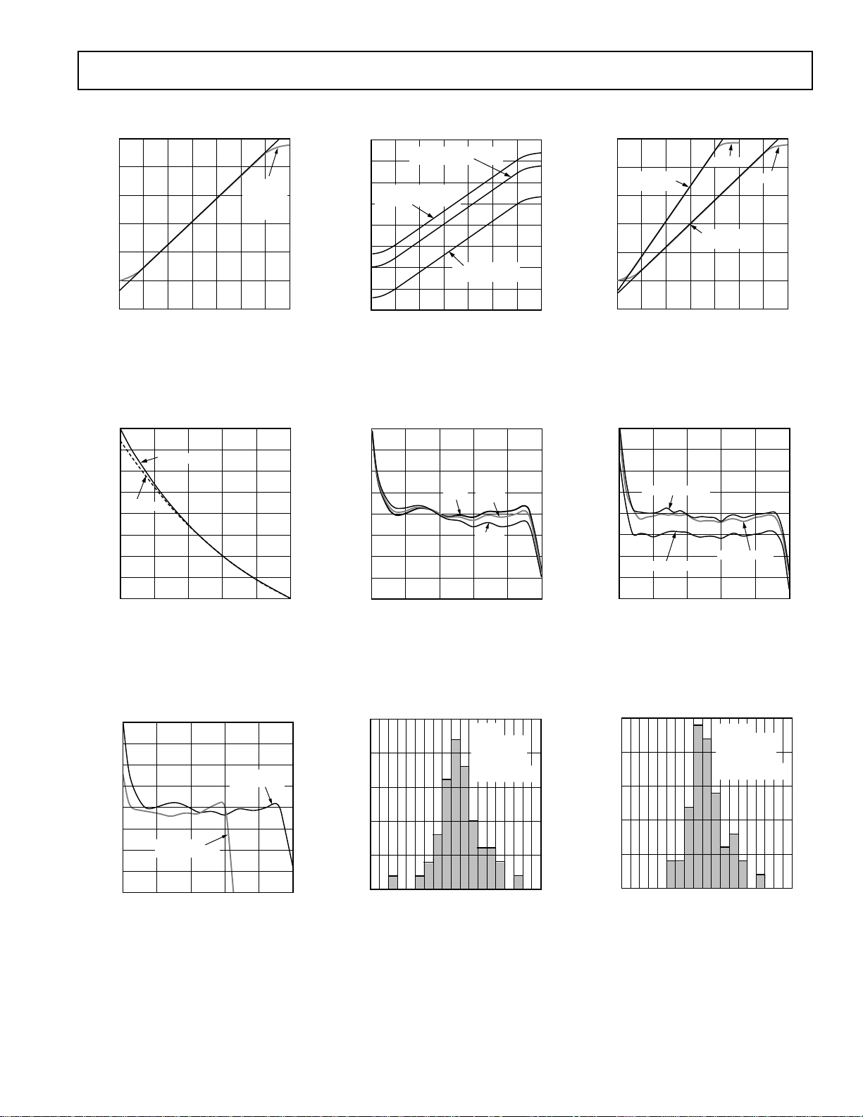
Figure 1. Gain vs. VGN
40
37.5
35
32.5
30
27.5
GAIN SCALING – dB/V
25
22.5
20
1.25
THEORETICAL
ACTUAL
1.5 1.75 2 2.25 2.5
V
REF
= 2.5 V (20 dB/V Scaling), f = 1 MHz, RL = 500 V, CL = 5 pF, TA = +258C, VSS = 65V)
REF
60
50
40
30
20
GAIN – dB
10
0
–10
–20
0.1
Figure 2. Gain vs. VGN for Different
Preamp Gains
2.0
1.5
1.0
0.5
0
–0.5
GAIN ERROR – dB
–1.0
–1.5
–2.0
0.2
G (PREAMP) = +14dB
(0dB – +48dB)
G (PREAMP) = +20dB
(+6dB – +54dB)
DSX ONLY
(–14dB – +34dB)
0.5 0.9 1.3 1.7 2.1 2.5 2.9
VGN – Volts
–40°C
+25°C
+85°C
0.7 1.2 1.7 2.2 2.7
VGN – Volts
Figure 3. Gain vs. VGN for Different
Gain Scalings
Figure 4. Gain Scaling vs. V
2.0
1.5
1.0
0.5
0
–0.5
GAIN ERROR – dB
–1.0
–1.5
–2.0
0.2
Figure 7. Gain Error vs. VGN for
Different Gain Scalings
REV. 0
VREF = 1.67V
0.7 1.2 1.7 2.2 2.7
30dB/V
VGN – Volts
REF
20dB/V
VREF = 2.50V
Figure 5. Gain Error vs. VGN at
Different Temperatures
25
20
15
10
PERCENTAGE
5
0
–0.6
–1.0
–0.8
–0.4 –0.2 0.1 0.3 0.5 0.7 0.9
DELTA GAIN – dB
N = 50
VGN1 = 1.0V
VGN2 = 1.0V
∆G(dB) =
G(CH1) – G(CH2)
Figure 8. Gain Match; VGN1 = VGN2 =
1.0 V
–5–
Figure 6. Gain Error vs. VGN at
Different Frequencies
Figure 9. Gain Match: VGN1 = VGN2 =
2.50 V

AD604–Typical Performance Characteristics (per Channel)
VGN – Volts
210
0.1
190
170
150
130
110
90
0.5 0.9 1.3 1.7 2.1 2.5 2.9
+85°C
+25°C
–40°C
NOISE – n V / √Hz
NOISE – p V / √Hz
FREQUENCY – Hz
770
745
740
760
765
750
755
100k 1M 10M
VGN = 2.9V
VGN – Volts
dB
40
20
0
0
1.2
35
30
25
15
10
5
0.4 0.8 1.6 2.0 2.4 2.8
RS = 240Ω
(Unless otherwise noted G (preamp) = +14 dB, V
= 2.5 V (20 dB/V Scaling), f = 1 MHz, RL = 500 V, CL = 5 pF, TA = +258C, VSS = 65V)
REF
50
VGN = 2.5V
40
30
20
10
0
GAIN – dB
–10
–20
–30
–40
–50
100k
VGN = 1.5V
VGN = 0.5V
VGN = 0.1V
VGN = 0.0V
VGN = 2.9V
1M 10M 100M
FREQUENCY – Hz
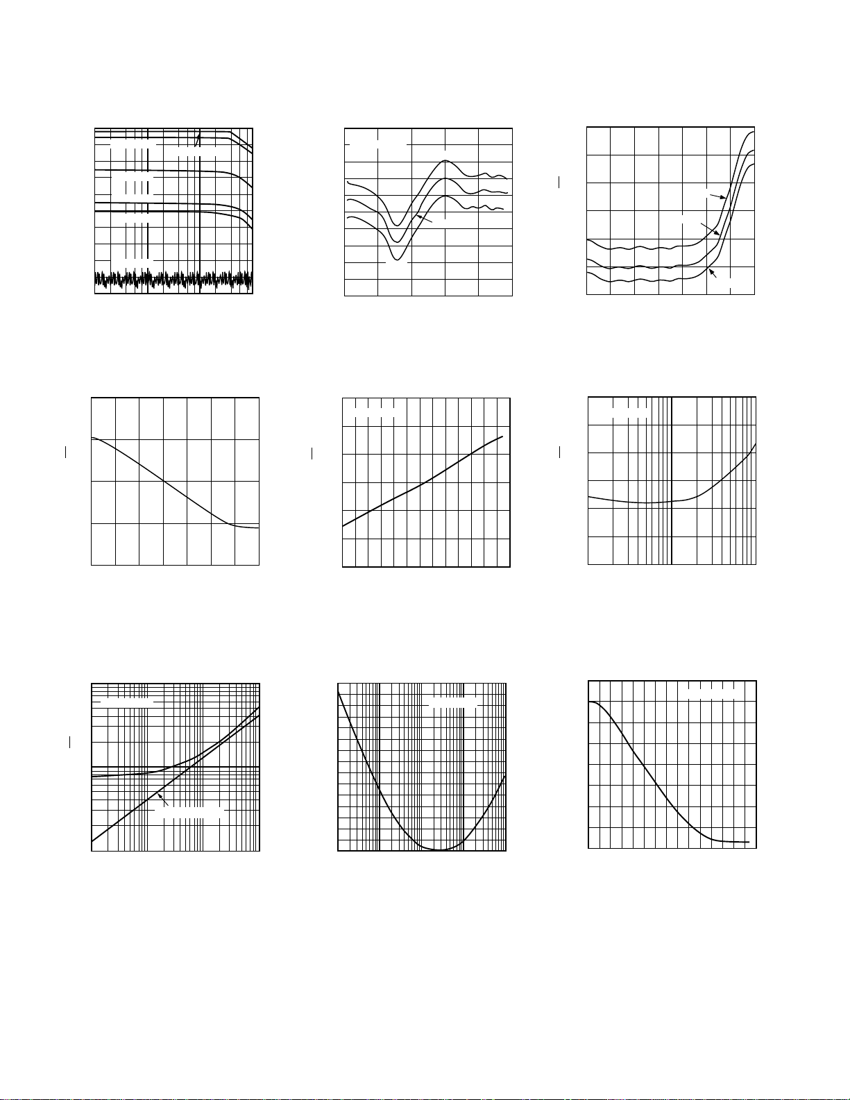
Figure 10. AC Response
1000
100
10
NOISE – n V / √Hz
1
2.55
2.54
2.53
2.52
2.51
2.50
– Volts
OUT
2.49
V
2.48
2.47
2.46
2.45
VOCM = 2.50V
+85°C
0.2
0.7 1.2 1.7 2.2 2.7
–40°C
+25°C
VGN – Volts
Figure 11. Output Offset vs. VN
900
VGN = 2.9V
850
800
750
700
NOISE – p V / √Hz
650
Figure 12. Output Referred Noise vs.
VGN
0.1
0.1 2.9
0.5 0.9 1.3 1.7 2.1 2.5
VGN – Volts
Figure 13. Input Referred Noise vs.
VGN
10
VGN = 2.9V
1
NOISE – n V / √Hz
0.1
1101k100
Figure 16. Input Referred Noise vs.
R
SOURCE
R
R
SOURCE
SOURCE
– Ω
ALONE
600
–40 –20 20 40 60
080
TEMPERATURE – °C
Figure 14. Input Referred Noise vs.
Temperature
16
15
14
13
12
11
10
9
dB
8
7
6
5
4
3
2
1
110
Figure 17. Noise Figure vs. R
VGN = 2.9V
100
RIN
1k
10k
SOURCE
90
Figure 15. Input Referred Noise vs.
Frequency
Figure 18. Noise Figure vs. VGN
REV. 0–6–
 Loading...